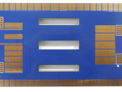
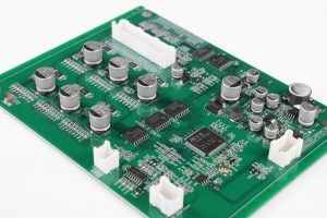
An aluminum frame PCB stencil holds a patterned metal foil under tension so solder paste can be printed onto PCB pads before component placement. The aluminum is the support frame, not normally the printing foil. At EBest Circuit (Best Technology), we supply custom SMT stencils and PCB assembly support. For your project, the useful starting points are printer compatibility, aperture geometry, foil thickness and the final panel layout.
What Is an Aluminum Frame PCB Stencil?
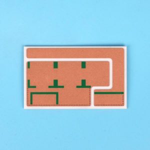
A framed PCB stencil combines three working parts: a rigid frame, a tensioned mesh border and a thin metal foil containing openings that correspond to the solder-paste pattern. The squeegee moves paste across the foil; the openings control where paste reaches the board. After separation, the paste deposits remain on the pads.
The distinction between frame material and PCB stencil material matters when ordering. Aluminum provides a lightweight, rigid support. Stainless steel is commonly used for the PCB stencil foil because it can be fabricated with fine openings and withstand repeated printing and cleaning. A steel foil does not turn the finished circuit board into an aluminum PCB.
A PCB framed stencil is a complete mounted tool, whereas a stencil blank is an unpatterned starting material. If you need a working circuit board stencil, specify the aperture file and mounting arrangement, not just the frame dimensions.
Framed vs Frameless Stencil: Which Suits Your Production?
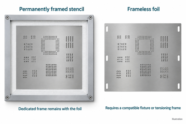
A permanently framed tool is useful for repeat builds on compatible equipment. A frameless foil can suit either a manual fixture or a reusable tensioning system, but those are different setups. Frameless does not automatically mean unsuitable for production.
Option
Best fit
What to check
Permanently framed stencil
Recurring assemblies with a dedicated tool
Printer fit, stored-frame space, mesh and bond condition
Foil mounting interface, tensioning procedure and changeover time
Unframed foil in a manual fixture
Low-volume builds and development work
Flat support, registration and repeatability of the fixture
For a frameless PCB stencil printer, confirm the foil attachment system before ordering. A foil made for one tensioning system may not fit another. Prototype SMT stencils should therefore be selected around the intended printing process, not around a fixed prototype-versus-production label.
What Frame Size Fits Your Stencil Printer?
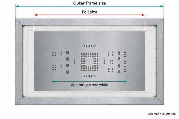
There is no single PCB stencil standard size that fits every printer. The outer frame must fit the machine clamps, while the usable printing area must accommodate the complete panel and squeegee travel. Frame profile, thickness, mounting direction and underside-cleaning clearance also affect compatibility.
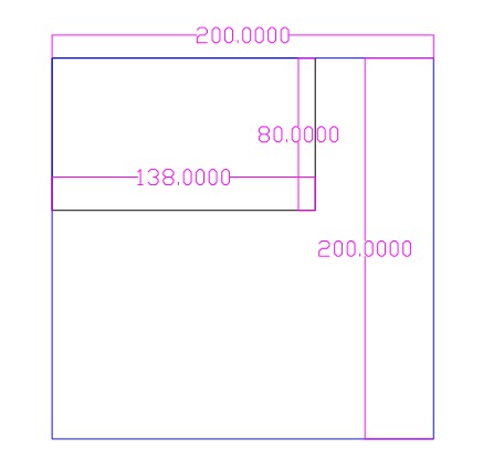
An SMT stencil frame drawing should distinguish the outer frame size, foil size and aperture-pattern envelope. The actual printable area is further limited by bonding margins and the printer mechanism; it is not simply the entire foil. Send the printer model or approved mounting drawing instead of ordering a frame from PCB length and width alone.
A PCB stencil holder or PCB stencil jig must support registration without bending the foil or board. For our FR4 printed circuit boards, use the released panel drawing, including rails, orientation and fiducials, when preparing the stencil. Changing the panel after cutting can make an otherwise accurate stencil unusable.
How to Choose PCB Stencil Thickness?
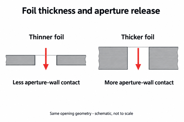
Choose thickness from the paste-volume requirements of the component mix and the release behavior of the smallest openings. A thicker foil provides more theoretical paste volume for the same aperture, but also increases the wall area that the paste must release from. More thickness is not automatically better.
Our custom SMT stencil options cover a foil-thickness range of 0.10-0.60 mm across different stencil applications, subject to engineering review. This capability range is not a recommended thickness range for every fine-pitch SMT board. We also offer step-up and step-down stencil options where different areas need different deposit volumes.
For mixed fine-pitch ICs and larger terminals, evaluate a uniform foil first, then consider local thickness changes if the requirements conflict. Step locations need clearance from nearby apertures and suitable squeegee access. Component pitch alone is not enough to select PCB stencil thickness.
How Does SMT Stencil Aperture Design Affect Paste Release?
SMT stencil aperture design determines both deposit geometry and release conditions. For a rectangular opening with length L, width W and foil thickness t, area ratio is LW / [2t(L + W)]. Aspect ratio is W/t when W is the smaller opening dimension. These describe different geometric relationships.
Illustrative opening
Foil thickness
Area ratio
Theoretical aperture volume
0.30 × 0.60 mm
0.10 mm
1.00
0.018 mm³
0.30 × 0.60 mm
0.15 mm
0.67
0.027 mm³
These calculated values illustrate geometry, not a guaranteed process window or measured deposit. Actual transfer depends on paste, aperture-wall condition, separation settings and board support. A PCB stencil thickness calculator cannot replace a print trial on the intended assembly.
For large thermal pads, multiple smaller windows may help distribute paste more appropriately than one large opening. For small pads, excessive aperture reduction can make release harder. PCB stencil design should use the component manufacturer’s land-pattern guidance, target deposit and assembly process together; a universal reduction percentage is not suitable for every footprint.
Which Fiducials and Panel Details Must Match?
PCB stencil fiducials let the printer align the foil pattern to the board. Their locations, optical contrast and marking method must suit the vision system. A fiducial is not necessarily an open hole: etching, filling or other marking arrangements depend on the printer and stencil specification.
For double-sided assemblies, identify top and bottom paste files explicitly and confirm viewing direction. Do not mirror a file merely because it is named bottom. The manufacturing output convention and assembly orientation must agree. When both sides share one foil, the printer’s working area, orientation and separation between patterns need approval.
Keep the PCB paste layer, panel drawing and assembly revision synchronized. The solder-mask layer is not a substitute for the paste layer: mask openings expose board features, while paste apertures define deposits for assembly.
How Is a Laser Cut PCB Stencil Made?
A laser cut PCB stencil is produced by cutting the approved aperture pattern into metal foil, applying the specified finishing operations and mounting the foil to its support system. In a permanently framed construction, the foil and mesh bond must maintain the required tension and flatness during use.
Our PCB stencil service includes laser-cut, etched, framed and unframed constructions, as well as electropolishing options. For a laser cut SMT stencil, electropolishing can improve aperture-wall condition, but it does not correct the wrong aperture geometry, foil thickness or panel file. The finishing requirement belongs in the order specification.
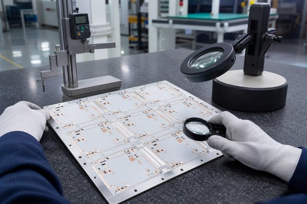
Before release, agree on the features that need verification: aperture dimensions and positions, foil thickness, image orientation, frame compatibility, bond condition and tension where specified. For fine-feature work, clarify the measurement method and acceptance criteria rather than assuming the word precision defines them.
How to Use a PCB Stencil?
The basic sequence is alignment, printing, controlled separation and deposit inspection. For a new framed tool, a short first-article print check is more useful than assuming that successful clamping proves process readiness.
Confirm the stencil revision, print side and matching PCB panel.
Support the board and align the apertures to the pads using the printer’s specified registration method.
Apply compatible solder paste and use the established squeegee and separation settings for the assembly.
Inspect deposit alignment, bridging, missing paste and consistency before placing components.
Adjust the process or aperture design from the observed defect, rather than compensating for every problem with more pressure.
SMT solder paste stencils are printing tools, not reflow fixtures. The stencil is removed before placement and reflow. Through our PCB assembly services, we support SMT, through-hole and mixed assemblies; discuss stencil supply together with your assembly files when you need a coordinated PCB and PCBA order.
How Should Framed Stencils Be Cleaned and Stored?
Use a cleaning method compatible with the solder paste, foil, mesh and bonding adhesive. Residue inside an aperture can reduce the next deposit, while contamination beneath the foil can contribute to smearing. Follow the applicable cleaning-equipment and chemistry instructions, and protect personnel according to the relevant safety information.
Do not scrape fine openings with tools that can alter their geometry. After cleaning, check for blocked apertures, dents, corrosion, lifted bonding and mesh damage. A visibly clean foil is not automatically a flat, tensioned tool.
Store each tool by design, side and revision in a protected SMT stencil rack or equivalent support. Prevent contact with the active foil area. Reuse depends on condition and validated printing performance, not a universal number of print cycles. A replacement foil must also match the original mounting system.
What Affects the Price of a Framed PCB Stencil?
Price depends on frame size, foil specification, aperture complexity, finishing, step features, inspection requirements and delivery arrangements. A low tool price can be poor value if it requires a new holder, cannot fit the printer or has to be remade after a panel revision.
Compare quotations against the same drawing and scope. Ask whether the price includes the aluminum frame, patterned foil, mounting, specified finishing and inspection. For repeat orders, confirm whether an existing frame can be reused and whether that service is actually included.
For suitable stencil orders, we can provide turnaround as fast as one working day. Availability depends on the design, finishing and order review; production time is separate from transport time. Tell us the required arrival date so that the quotation can address both.
What Files Do We Need for Your Custom Stencil?
For a custom aluminum frame PCB stencil, send the released paste-layer data and final panel information first. We accept Gerber and supported PCB/CAD design files. A PDF can explain dimensions and notes, but a drawing alone may not contain the complete aperture geometry needed for manufacture.
Input
Include
Design identity
Part number, revision, top/bottom side and units
Aperture data
Paste Gerber or supported design files, approved modifications and critical features
Panel and alignment
Final panel drawing, rails, fiducials and print orientation
Printer interface
Machine model, outer frame dimensions, frame profile and clamping requirements
Foil and finishing
Requested thickness, step regions, surface treatment and inspection criteria
Order scope
Quantity, stencil-only or PCB/PCBA supply, destination and required arrival date
If the thickness or aperture treatment is not yet defined, identify the fine-pitch devices and larger solder-volume features for review instead of guessing a specification. Send your aluminum frame PCB stencil requirements to sales@bestpcbs.com. Our team can discuss the stencil construction and manufacturing scope with you before quotation.
Choosing a high-frequency PCB manufacturer in Israel requires a comparison of the actual fabrication site, RF material controls, stackup ownership, impedance verification, quality records, and delivery route. An Israeli address may identify a factory or a local engineering and sourcing company, so the quotation must name where the bare board will be built.
Use the same released stackup, material requirements, test limits, quantities, and delivery destination when requesting quotes so differences in capability, evidence, and lead time can be compared on equal terms.
Which High-Frequency PCB Manufacturers in Israel Can You Consider?
Three Israel-based suppliers have relevant public RF or microwave information, but they do not represent the same supply model. PCB Technologies and Eltek identify manufacturing operations in Israel; APEX PCB presents an Israel-based engineering and supply service supported by a global supplier network.
Manufacturer
Address
Manufacturing Capabilities
Lead Time
Advantages
PCB Technologies
7 Ahoman St., Migdal HaEmek, Israel
RF and microwave boards, controlled impedance, RF materials, hybrid constructions, prototypes, PCB fabrication, and assembly
Confirmed after stackup, material availability, inspection scope, quantity, and assembly review
Direct coordination with an Israeli fabrication and assembly operation for engineering-intensive RF projects
Eltek
20 Ben Zion Gelis St., Petah Tikva, Israel
Rigid and rigid-flex boards, multilayers, mixed-material low-Dk and low-Df constructions, and RF and microwave applications
Quoted for the approved material set, construction, test plan, quantity, and factory loading
Israeli PCB manufacturing route for complex rigid, rigid-flex, and mixed-material RF constructions
APEX PCB
Kibbutz Hazorea, Israel
High-frequency boards, controlled multilayer structures, material selection, impedance modeling, prototype coordination, and quality control
Depends on the named partner factory, material allocation, production route, inspection, and international delivery
Israel-based technical coordination with access to a wider supplier network for prototype and production sourcing
What Should You Compare Between Israel High-Frequency PCB Manufacturers?
Compare suppliers against one released design and one acceptance package. This exposes differences in factory responsibility, material control, RF engineering, evidence, delivery, and total commercial risk without mixing unlike quotations.
Fabrication site: Record the factory name, street address, and processes performed there, including lamination, drilling, plating, imaging, etching, surface finish, electrical test, and final inspection.
Material control: Compare approved laminate grades, prepregs, bondplies, copper foils, thickness availability, storage, lot traceability, and substitution rules.
RF engineering: Confirm who creates the production stackup, calculates impedance geometry, approves trace-width adjustments, designs coupons, and closes technical exceptions.
Quality evidence: Define the material certificates, impedance results, microsections, dimensional reports, electrical-test records, and first-article documents supplied with the order.
Delivery route: Compare engineering review, material procurement, fabrication, inspection, assembly, freight, customs, and receiving inspection to the same arrival point.
Change control: Require written approval before changing the factory, laminate, dielectric thickness, copper foil, stackup, artwork compensation, surface finish, coupon, or test method.
A supplier remains on the shortlist only when its factory, process, evidence, and schedule all match the same project requirements.
Can the Manufacturer Support Your RF and Microwave PCB Requirements?
The manufacturer must support the complete signal path, not only purchase a high-frequency laminate. Review whether its processes can hold the conductor geometry, dielectric construction, plated features, reference planes, and surface interfaces used by the design.
Controlled transmission lines: Provide target impedance, tolerance, line type, reference plane, nominal geometry, and affected layers. The factory should return production dimensions before release.
Multilayer registration: Ask for achievable layer-to-layer registration on the proposed panel and material system because misregistration changes trace-to-plane geometry and via capture.
Advanced vias: Specify finished hole, aspect ratio, via-in-pad filling, blind or buried spans, backdrill depth, stub limit, and sequential-lamination requirements.
RF transitions: Mark connector launches, grounded coplanar sections, cavities, plated edges, castellations, and controlled-depth features, then define how their dimensions will be inspected.
Surface control: State copper-profile restrictions, finish thickness, solder-mask clearance around RF conductors, flatness, cleanliness, and wire-bondable areas when applicable.
Assembly interface: Separate bare-board acceptance from assembled RF performance. Define connector installation, shielding, thermal interfaces, cleaning, and functional or RF tests.
Capability is credible when the factory can return a manufacturable stackup, controlled dimensions, inspection method, and acceptance record for every critical RF feature.
Which Materials and PCB Structures Should RF PCB Manufacturers in Israel Support?
The required materials follow the loss budget, frequency, power, thermal environment, mechanical design, and production volume. A qualified manufacturer should support the exact approved grades or propose alternatives with comparable electrical and processing data for engineering approval.
Low-loss hydrocarbon ceramic laminates: Confirm grade, thickness, copper type, bondply, and panel construction for designs where insertion loss and phase consistency matter.
Low-loss epoxy systems: Use these where the measured performance, multilayer process, assembly conditions, and cost fit the actual frequency and geometry.
Hybrid stackups: Combining RF laminate with FR-4 can control cost and thickness, but the factory must manage bonding, resin flow, z-axis expansion, registration, and material movement.
Rigid-flex or flex structures: Confirm controlled dielectric, copper, coverlay, bend geometry, launch design, and transition capability at the named facility.
Metal-backed structures: High-power RF boards may need heat spreaders, metal cores, coins, cavities, or bonded carriers with separately defined thermal and grounding interfaces.
The approved stackup should name the material grade, dielectric thickness, copper foil, bond system, finished copper, and permitted alternatives. Family names alone do not control the finished board.
How Can You Check Whether a Supplier Can Meet Your Impedance and Signal Loss Requirements?
Set impedance and loss as measurable acceptance requirements before fabrication. The supplier should model the production stackup, obtain approval for geometry changes, and use coupons or board-level structures that represent the critical signal paths.
Lock the inputs: Use the actual laminate grade, process-relevant Dk, pressed dielectric thickness, finished copper, copper profile, trace width, spacing, solder mask, reference-plane distance, and surface finish.
Control artwork changes: Require a returned impedance table showing customer dimensions, production dimensions, calculated values, tolerance, and approval status.
Use representative coupons: Place structures on the same panel with the same layer, dielectric, copper, and processing conditions as the board.
Separate impedance from loss: TDR verifies characteristic impedance and discontinuities; it does not prove insertion loss, return loss, phase response, or connector performance.
Define RF measurements: For loss-sensitive designs, specify frequency range, fixture, de-embedding method, reference structure, sample quantity, limits, and report format.
Correlate results: Compare coupon data, board measurements, material lots, microsections, and production geometry.
Accept the lot only against the agreed method and limits. A capability statement or one TDR screenshot cannot replace a controlled measurement plan.
How Should You Verify the Quality of High-Frequency PCBs Before Ordering?
Quality verification should begin with process review, continue through a representative prototype, and finish with evidence tied to the delivered lot. Each checkpoint should show whether the construction matches the RF model and whether the factory can repeat it.
Approve the factory and route: Confirm the fabrication site, material source, stackup owner, subcontracted processes, inspection responsibility, and change-control contact.
Complete RF-focused DFM: Review stackup, impedance tables, via structures, backdrill, registration, copper balance, panelization, finish, solder-mask clearances, and coupons.
Build a representative prototype: Use the intended material family, copper profile, finish, critical geometry, and manufacturing site.
Inspect the first build: Compare dimensions, microsections, impedance data, material records, electrical testing, visual inspection, and required RF measurements with the released limits.
Correlate assembly performance: Document connectors, soldering, fixtures, calibration, test conditions, and limits so failures can be assigned to the board, assembly, or test interface.
Freeze the qualified configuration: Record deviations, tooling assumptions, coupon design, test method, and reporting format. Requalify changes that affect the RF construction.
This sequence turns qualification into a repeatable release process instead of a one-time sample approval.
What Inspection and Test Reports Should You Request From a High-Frequency PCB Manufacturer?
Request reports that close a specific manufacturing risk. The final document package should connect the approved material, finished geometry, electrical continuity, impedance, and RF measurements to the same purchase order and lot.
Material records: Require laminate and prepreg grade, lot identity, thickness, copper type, supplier certificate, and approved substitution record.
Stackup release: Retain the final construction, pressed dielectric targets, finished copper, impedance geometry, artwork compensation, and approvals.
Impedance report: Request coupon ID, layer, line type, target, tolerance, measured values, method, equipment, date, lot association, and result.
Microsection report: Define sampled locations and dimensions such as dielectric thickness, copper, plating, registration, hole quality, via fill, and backdrill stub.
Electrical-test report: Confirm netlist source, method, quantity tested, criteria, and lot result. Continuity does not replace impedance or RF testing.
Dimensional inspection: Identify critical trace, hole, routing, cavity, edge-plating, flatness, and connector-interface dimensions with sampling and limits.
RF test report: Specify frequency sweep, fixture, calibration, de-embedding, S-parameters, sample size, environmental condition, and limits before quotation.
An order-linked evidence pack is more useful than certificates that cannot be matched to the delivered boards.
Which Certifications Should You Check When Comparing PCB Manufacturers in Israel?
Check certifications against the legal entity, factory address, scope, revision, and validity period required by the project. A certificate supports the system named in its scope; it does not replace board-specific material, process, inspection, or test evidence.
ISO 9001: Verify the stated quality-management scope and certified site. The order still needs product-specific acceptance criteria.
AS9100: Aerospace and defense programs may require a covered entity, traceability, risk controls, configuration management, and customer approvals.
ISO 13485: Medical projects should confirm that the relevant PCB or PCBA work falls within the certified medical-device quality scope.
IATF 16949: Automotive programs should verify site scope, customer-specific requirements, production controls, and change notification.
UL recognition: Match material, flammability, thickness, copper, coating, and marking conditions to the applicable factory file.
IPC requirements: State the applicable performance and acceptability documents, class, amendment, and customer additions. IPC documents are product requirements, not factory certifications.
The correct certificate covers the named site and service. The correct board evidence proves compliance with the released order.
How Should You Compare Prototype and Production Lead Times?
Compare schedules by milestone rather than one turnaround number. Prototype work often spends more time on engineering closure, while production adds material allocation, capacity planning, lot inspection, assembly, and shipment controls.
Milestone
Prototype
Production
Buyer Check
Engineering release
DFM, stackup, impedance geometry, coupon, and exception approval
Frozen revision, approved deviations, tooling, inspection plan, and change controls
Date when fabrication can start with no open technical questions
Material allocation
Available stock, minimum panel purchase, or expedited procurement
Reserved quantity, lot strategy, shelf life, approved alternatives, and reorder coverage
Grade, quantity, allocation date, and substitution approval status
Fabrication
Small-lot route with required laminations, drilling, plating, finish, and tests
Scheduled panels, process capacity, sampling, yield response, and lot release
Business days by process, including queue time and weekends
Inspection
First-article records and customer review before assembly or shipment
Lot reports, deviation closure, source inspection, and release authorization
Report date, review owner, approval window, and rework contingency
Delivery
Courier shipment or transfer to assembly and engineering evaluation
Scheduled freight, customs, buffer stock, receiving, and line-side date
Committed arrival location and responsibility for transit delays
Request dates for each milestone and compare the committed arrival date, not a fabrication time that excludes engineering, material, inspection, or transport.
What Factors Can Affect High-Frequency PCB Lead Time in Israel?
Lead time changes when the design requires scarce materials, repeated lamination, specialized drilling or plating, extensive evidence, assembly, or international logistics. The quotation should show which dependency controls the schedule and when it becomes firm.
RF material availability: Nonstandard grades, thicknesses, copper profiles, bondplies, and minimum purchase quantities can delay release. Confirm allocated stock rather than catalog availability.
Engineering closure: Open stackup, impedance, trace-compensation, panelization, coupon, or finish questions stop the manufacturing clock. Assign owners and approval deadlines.
Construction complexity: Hybrid materials, rigid-flex structures, sequential lamination, high layer counts, tight registration, cavities, and controlled-depth features add operations.
Via processing: Small drills, laser microvias, via fill, planarization, backdrill, and multiple plating cycles require specific equipment and inspection capacity.
Test scope: Impedance coupons, microsections, dimensional layouts, VNA measurements, source inspection, and customer approval add named milestones.
Assembly inputs: Component availability, RF connectors, shielding, thermal hardware, stencils, programming, fixtures, and functional testing can control the PCBA date.
International delivery: For partner or overseas factories, include export documents, freight, customs clearance, Israeli receiving days, and nonconformance contingency.
A reliable schedule identifies the longest dependency and its owner. A short number without material status, release conditions, and delivery endpoint is not a usable commitment.
What Information Should You Provide When Requesting Quotes From High-Frequency PCB Manufacturers in Israel?
A comparable RFQ gives every candidate the same design revision, material rules, electrical limits, quality evidence, quantity, assembly scope, and delivery destination. Missing inputs force suppliers to quote different assumptions and hide cost or schedule risk.
Fabrication data: Supply Gerber or ODB++, fabrication drawing, drill data, netlist, impedance table, stackup, panel requirements, revision, and file-precedence notes.
Material specification: Name laminate, prepreg or bondply, dielectric thickness, copper foil and profile, finished copper, approved alternatives, and substitution approval.
RF requirements: State frequency, line type, impedance and tolerance, loss or S-parameter limits, power, reference structures, method, fixture, and report format.
Mechanical features: Identify thickness, dimensions, hole tolerances, via structures, backdrill, cavities, plated edges, controlled depth, flatness, and connector interfaces.
Quality package: Define IPC class or customer criteria, material records, coupons, microsections, dimensional reports, electrical testing, first-article inspection, RF testing, traceability, and retention.
Commercial quantities: Request prototype, pilot, and production prices with tooling, testing, engineering, material minimums, assembly, packaging, freight, and taxes separated. Include the BOM, placement data, and assembly drawings when PCBA is required.
Delivery terms: Provide the Israeli delivery address, required arrival date, Incoterm, freight method, customs responsibility, partial-shipment rules, and documents.
Supplier response: Require factory identity, proposed stackup, material status, production lead time, delivery lead time, exclusions, subcontracted steps, and quotation validity.
FAQs About High-Frequency PCB Manufacturers in Israel
Q1: When should the manufacturer review the RF stackup?
A1: Request review before routing is frozen. The factory should return the production stackup, controlled-impedance geometry, coupon method, material status, and exceptions before tooling.
Q2: Can the manufacturer change controlled-impedance trace widths?
A2: Only with written approval. The returned impedance table should show customer dimensions, proposed production dimensions, calculated values, tolerances, and affected layers.
Q3: Is a TDR report enough to qualify an RF PCB supplier?
A3: No. TDR checks impedance and discontinuities; it does not prove insertion loss, return loss, phase, material identity, plating reliability, or assembled RF performance.
Q4: Can an RF laminate and FR-4 be combined in one stackup?
A4: Yes, when bonding, resin flow, z-axis expansion, registration, copper balance, and RF performance are validated for the exact construction. The approved stackup should identify every material and interface.
Q5: Should the same factory build prototypes and production boards?
A5: Using one factory reduces transfer variables but is not mandatory. If production moves, freeze the material, stackup, artwork compensation, coupons, tests, limits, and deviations, then requalify the transferred build.
Choose the supplier that can build the released material and stackup, measure the required electrical performance, provide order-linked quality records, and commit to a complete delivery schedule.
If an overseas manufacturing route is acceptable, EBest Circuit is a China-based PCB and PCBA supplier serving international projects. Send your Gerber or ODB++, stackup, RF requirements, quantity, assembly scope, test plan, delivery address, and target date to sales@bestpcbs.com for a free DFM review and quotation.
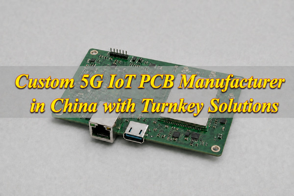
EBest Circuit is a custom 5G IoT PCB manufacturer in China offering PCB fabrication, component sourcing, assembly, programming and testing. From early prototypes to repeat production orders, you can purchase bare boards or combine the work in a turnkey order.
We support boards for industrial gateways, routers, edge devices and remote monitoring equipment. Whether you supply the 5G modules or ask us to source the complete BOM, we coordinate the board build and assembly around your design, quantities and delivery requirements.
Send your Gerber files and BOM for a free DFM review. We can check manufacturing details, identify sourcing questions and prepare a quotation for the services you need.
What 5G IoT PCB Manufacturing and Assembly Services Do We Provide?
Our 5G IoT PCB manufacturing services cover bare boards, populated PCBs and box assembly. Choose the stages you need us to handle; you can retain your existing design or sourcing arrangements.
Custom PCB fabrication: Multilayer and HDI manufacturing support the routing and via requirements of compact boards. Provide the stackup, material, copper, finish and impedance specifications so we can review the complete construction.
Prototype and production builds: Start with samples for fit and functional evaluation, then order the accepted revision for small-batch or mass production. Changes found during testing should be incorporated before the next batch.
SMT and through-hole assembly: Assembly can combine dense IC packages and compact passives with through-hole connectors. Package pitch, board layout and joint access determine the soldering and inspection requirements.
Component sourcing: Full turnkey procurement covers the BOM; partial turnkey lets you supply selected modules or other parts. Exact part numbers and approved alternatives keep purchasing aligned with your design.
Programming, functional testing and box assembly: Add these services when the order requires programmed boards or assembled units. Supply firmware, test limits, fixture requirements and enclosure drawings so the deliverables are defined before production.
What 5G IoT PCB Manufacturing Capabilities Can We Support?
Our PCB fabrication capabilities include multilayer boards, HDI features and controlled impedance. The values below are process limits; the combination of features in your board needs engineering confirmation.
Manufacturing feature
Capability
Standard trace / space
4 / 4 mil
HDI trace / space
2 / 2 mil
Standard minimum hole diameter
0.20 mm
HDI minimum hole diameter
0.10 mm
Impedance tolerance above 50 Ω
±10%
Impedance tolerance at or below 50 Ω
±5 Ω
What 5G IoT Applications Can We Support?
Our services support several types of 5G-connected equipment. Each puts different demands on the board layout, component selection and assembly:
Industrial gateways and routers: Module integration, multiple interfaces and external connectors can combine dense routing with mechanical constraints. Include the enclosure and connector positions in the fabrication and assembly review.
Edge computing devices: Processor and memory routing, power delivery and heat dissipation influence the board construction. Identify critical interfaces and cooling arrangements so the stackup and assembly access can be reviewed together.
Remote monitoring and tracking equipment: Compact packaging, antenna placement and power requirements can constrain component layout. Supply the operating conditions and mechanical drawings with the board files.
Connected meters and control equipment: Communication circuits share the board with sensing, power or field connections. Define the required clearances, connections and functional checks; the product’s electrical requirements remain part of the acceptance plan.
Can We Support 5G IoT PCB Prototypes and Mass Production?
We support PCB prototyping, small-batch production and mass production. You can evaluate a small batch before committing to a larger order, then carry the approved design and test requirements into repeat builds.
Prototype assembly: Use the first boards to check connector fit, programming access and product operation. Record any layout, component or firmware changes so the next batch incorporates what your team learned.
Small-batch production: Build a limited batch from the revised files to assess assembly consistency and the test procedure. Repeated rework or test failures need investigation before you increase the order quantity.
Sample approval: Your team reviews the samples and test records, then confirms the PCB revision, BOM, permitted alternatives and acceptance criteria. This approval gives production a clear specification to follow.
Mass production: We manufacture against the approved files. Agree on lot identification and delivery records so your receiving team can check each shipment and trace a problem to the relevant batch.
For repeat orders, tell us about changes to components, firmware or test limits before manufacturing starts. Even when the PCB layout stays the same, those changes can affect assembly or testing.
Can We Provide Component Sourcing and Turnkey 5G IoT PCB Assembly?
We can combine fabrication, BOM procurement and assembly in a turnkey order. The purchasing arrangement determines which parts EBest sources and which parts your team supplies.
Full turnkey: EBest sources the specified components and coordinates the PCB build and assembly. Send the full BOM and approved alternatives so availability can be reviewed before a delivery date is confirmed.
Partial turnkey: Supply selected items, such as modules or processors you already hold, and have EBest source the balance. Confirm quantities, packaging and arrival dates for your parts to avoid holding up assembly.
Consigned components: Your team provides the parts for assembly. Include exact part numbers, quantities and handling requirements so incoming checks can match them to the approved BOM.
For long-lead or obsolete parts, flag the affected BOM lines at quotation. We can review availability and proposed alternatives, but a substitute needs your engineering approval. Check the critical parts before committing to the production quantity.
How Do We Control Quality During 5G IoT PCB Manufacturing?
Our assembly quality checks cover incoming components, soldering and agreed functional tests. The inspection method depends on the defect being checked and whether the joint or circuit is accessible.
Incorrect or damaged incoming parts: Check identification and condition against the BOM before assembly. Resolve discrepancies before components enter the build.
Solder paste defects:SPI checks paste deposits before reflow, when a printing problem can still be addressed before soldering the components.
Placement and accessible solder defects: AOI supports inspection after assembly. Hidden BGA joints require a suitable method such as X-ray rather than an exterior visual check alone.
Board opens, shorts and impedance requirements: Specify the required electrical checks and impedance records with the fabrication order so results can be associated with the correct construction.
Product operation: Functional testing uses the agreed firmware, connections, test procedure and pass/fail limits. Specify any radio or network test separately, including its equipment and operating conditions.
Define the reports and lot or unit identification you need with delivery. Keep the accepted PCB revision, BOM and firmware connected to those records so a receiving or field issue can be investigated against the correct build.
How Do We Review 5G IoT PCB Designs Before Production?
A missing drill detail can hold up fabrication; a BOM mismatch can leave an assembly line waiting for the correct part. Our free DFM review, together with assembly checks, helps resolve these questions while the files can still be changed.
Check that the PCB files describe a buildable board. We review trace and space dimensions, hole sizes, via connections, copper clearances and the proposed stackup. For impedance-controlled nets, the drawing needs to identify the target and tolerance. If a fabrication note conflicts with the Gerber or drill data, we ask you to resolve the discrepancy before production. The output is a confirmed construction and a record of the changes you approved.
Match the components to the layout and assembly instructions. The BOM, placement data and assembly drawing should agree on reference designators, part numbers, orientation and unpopulated positions. A module variant with a similar name may have a different footprint or connector arrangement. We flag mismatches and review component spacing, solder-joint access and handling requirements so your team can correct the files before parts are fitted.
Keep programming and test connections accessible. A test point is of little use if a shield, connector or enclosure blocks it after assembly. Identify the programming interface and measurements needed for acceptance, then check probe access and fixture connections. Where access is restricted, agree on a layout change or an earlier test step. This gives the assembly team a usable test sequence and makes fixture preparation part of the schedule.
Send the latest revision of each file together and identify any unresolved design changes. We return manufacturing questions for your approval; RF performance, antenna operation and product compliance still require the appropriate design validation.
How Long Does 5G IoT PCB Manufacturing and Assembly Take?
For an initial schedule, allow about 10–12 days for qualifying 4–8-layer standard FR4 prototypes and about one week for PCBA. These are separate manufacturing references; the complete turnkey schedule also depends on component availability, test preparation and shipping.
Standard FR4 prototype fabrication is approximately 10 days for 4 or 6 layers and 12 days for 8 layers. These figures apply to orders below 1 m² meeting our standard FR4 specifications. HDI, special laminates and other nonstandard constructions need a separate schedule. Assembly timing is confirmed against the quantity and test scope, with the required boards and components available.
The main factors that can move your delivery date are:
Board construction: Layer count, via structure, material, finish and quantity affect fabrication. Identify special laminates and HDI requirements at quotation so availability and processing time can be checked before you commit to a date.
Parts availability: PCB fabrication and purchasing can overlap, but assembly needs a complete kit. A missing module or connector can delay the batch even when the bare boards are ready. Send exact part numbers and flag customer-supplied items early.
Testing and design changes: Programming files, fixtures and pass/fail limits must be ready for assembly. A late component substitution or revised test procedure can require another review before work continues.
Capacity and transport: Production loading, holidays, shipping and customs clearance affect arrival. Give us the date you need the boards at your site; WIP updates let you follow progress during manufacturing.
Case Analysis: From 5G IoT PCB Prototypes to Mass Production
Project background: In this hypothetical project, a hardware team needs 10 assembled prototypes for evaluation. After sample approval, it plans to begin mass production with an initial 100-board production order. Each board uses one customer-supplied 5G module and two specified interface connectors. EBest would fabricate the PCBs, source the remaining BOM and assemble the boards.
Requirements and challenges: The prototype batch therefore needs 10 modules and 20 interface connectors; the first production order needs another 100 modules and 200 connectors. These are fitted quantities, excluding assembly spares. Purchasing the production components before prototype approval risks committing parts to a design that may change. The team also needs programming access after assembly and a way to identify each tested board.
Our proposed solution: Check the board files and BOM first, then confirm the prototype kit and any spare-parts allowance. Assemble the 10 prototypes using one approved PCB, BOM and firmware revision. Record the programmed version and the agreed power-up and interface-test results against each board identifier. After customer evaluation, incorporate approved changes and confirm the components for the first 100-board production order before procurement and assembly proceed.
Output and acceptance: The requested prototype delivery consists of 10 assembled boards and 10 individual test records, plus the list of approved manufacturing changes. With one module and two connectors per board, the first production order has a fitted-parts requirement of 100 modules and 200 connectors. Mass production begins after sample approval and confirmation of the revised BOM. For subsequent orders, the approved PCB files, BOM, firmware and test procedure provide the manufacturing specification; any changes need approval before the next batch. Actual yield, test performance and delivery time would come from the completed build records.
Why Choose EBest as Your 5G IoT PCB Manufacturer?
Choose EBest when you want PCB fabrication, sourcing and assembly managed together. You can keep control of the design and critical parts while we coordinate the manufacturing work.
Less supplier coordination: A turnkey order brings the bare boards, purchased components and assembly under one contact. When a layout or part changes, you can resolve its effect on the complete order without forwarding separate instructions to several suppliers.
Quality checks matched to your board: Incoming inspection, SPI, AOI, X-ray and functional testing address different defects. We agree on the relevant coverage and records with you, helping your team inspect deliveries and investigate problems against the correct batch.
Delivery planning that includes the parts: We review material and component availability alongside fabrication and assembly. WIP updates help you follow the order and coordinate your own testing or product integration around manufacturing progress.
Engineering support before you commit to production: Free DFM review identifies manufacturing conflicts in the submitted files. Resolving them before fabrication helps avoid building boards that need an immediate revision.
Flexibility as quantities grow: Start with samples and continue to small-batch or mass production orders using the approved design. Full turnkey, partial turnkey and consigned-parts options let you choose how much procurement you retain at each stage.
What Files Are Required for a 5G IoT PCB Quote?
Send the files and specify whether you need bare boards or assembled units. Include prototype and production quantities, the destination and your required arrival date.
PCB fabrication: Gerber or ODB++ data, drill files, fabrication drawing, stackup and PCB specifications. Identify material, copper, finish and impedance requirements so the quotation matches the construction.
PCB assembly: BOM, pick-and-place data, assembly drawing and approved alternatives. Mark customer-supplied components and their availability so the sourcing split is clear.
Programming and testing: Firmware, test procedure, fixture requirements and acceptance criteria. Specify reports, lot identification and any enclosure work required with delivery.
Send your Gerber files, BOM, quantities, testing requirements and delivery date to sales@bestpcbs.com for a quotation and free DFM review.
FAQs About 5G IoT PCB Manufacturing
Q1: What happens if a BOM component is obsolete or unavailable?
A1: We can review availability and suggest alternatives. Your engineering team must approve a substitute before purchase, including any effect on fit, electrical operation, firmware or compliance requirements.
Q2: Can we change components after approving the prototype?
A2: Yes, but submit the updated BOM before the next order. Review the effect on layout, programming and test limits, and decide whether the change needs another sample build.
Q3: What should accompany a customer-supplied test fixture?
A3: Include connection instructions, compatible firmware, the test procedure and pass/fail limits. Confirm when the fixture will arrive so testing can begin when the assembled boards are ready.
Q4: Can EBest quote while some design files are still being revised?
A4: Send the available files and mark the open items. We can begin a preliminary review; the final price and schedule depend on the confirmed specifications, quantities, BOM and testing requirements.
Q5: How should we handle firmware changes between batches?
A5: Identify the firmware version and programming method for each order. If the new version changes product behaviour, update the test procedure and pass/fail limits before that batch is programmed.
Heavy copper PCB manufacturers in USA range from specialists in very thick conductors to suppliers that fabricate, assemble, and test complete boards. Choosing between them requires matching copper distribution, holes, and the complete layer stack to a process available at the required US site.
A 20 oz outer-layer power board needs a different manufacturing process from a 4 oz prototype supplied with components assembled. Copper capability determines which suppliers can build the board; engineering support, assembly services, and the prototype-to-production route determine which can deliver the complete order.
Top 15 Heavy Copper PCB Manufacturers in USA Compared
Amitron and Pro-Tech offer specialized thick-copper processes, while Cirexx, PNC, Sierra, and Gorilla combine fabrication with assembly services. Larger networks such as FTG, Sanmina, and TTM offer multiple production locations, making the selected factory as important as the company’s overall capability.
Manufacturer
Heavy Copper Capability
Advantages
Lead time
Services
1. AmitronElk Grove Village, IL
20+ oz finished copper
Mixed copper weights within one layer
Quoted per heavy-copper order
PCB fabrication
2. Pro-Tech Interconnect SolutionsChaska, MN
Extreme copper: above 20 to 120 oz
Local copper buildup for power paths and holes
Quoted per heavy-copper order
PCB fabrication; selective plating
3. AdvancedPCBMultiple US sites
Up to 4 oz inner; 20 oz outer
Mixed-weight layers with design support
Quoted per heavy-copper order
PCB design support; fabrication
4. Saturn ElectronicsRomulus, MI
Up to 20 oz
US double-sided and multilayer boards
Quoted per heavy-copper order
Bare PCB fabrication
5. Excello CircuitsAnaheim, CA
0.5–4 oz inner; 1–20 oz outer
Prototype and repeat-build support
Quoted per heavy-copper order
Prototype and production PCB fabrication
6. Cirexx InternationalUS in-house PCB site
Up to 4 oz inner; 6 oz outer
Layout, PCB assembly and test
Quoted per heavy-copper order
PCB layout; fabrication; assembly; testing
7. PNC Inc.Nutley, NJ
0.5–8 oz published range
Design and assembly at one US site
Quoted per heavy-copper order
PCB design; fabrication; assembly
8. Sierra CircuitsUS PCB sites
Advanced: up to 6 oz inner and finished outer
Advanced boards with assembly
Quoted per heavy-copper order
PCB fabrication; component sourcing; assembly
9. Gorilla CircuitsSan Jose, CA
4 oz stated maximum
In-house PCB, assembly and test
Quoted per heavy-copper order
PCB fabrication; assembly; testing
10. Bay Area CircuitsSilicon Valley, CA
Up to 4 oz inner; 5 oz outer, finished
Local and offshore PCB options
Quoted per heavy-copper order
PCB fabrication; offshore sourcing
11. Omega Circuits & EngineeringNew Brunswick, NJ
Up to 9 oz
Metal-based boards and heat sinks
Quoted per heavy-copper order
PCB fabrication; assembly with customer-supplied parts
12. American Standard CircuitsWest Chicago, IL
Heavy copper; confirm layer limits
Heavy copper and thermal board options
Quoted per heavy-copper order
PCB fabrication; global sourcing
13. FTG CircuitsCA, VA, MA and MN
Heavy copper; confirm site limits
US sites with varied PCB processes
Quoted per heavy-copper order
PCB fabrication; new-product introduction
14. SanminaSan Jose, CA; other US sites
Above 6 oz group offering; confirm US site
US new-product builds and global supply
Quoted per heavy-copper order
PCB fabrication; new-product introduction
15. TTM TechnologiesMultiple US sites; global network
2–12 oz auto offering; confirm US site
Auto power boards and multiple sites
Quoted per heavy-copper order
PCB fabrication
Manufacturer
Heavy Copper Capability
Advantages
1. AmitronElk Grove Village, IL
20+ oz finished copper
Mixed copper weights within one layer
2. Pro-Tech Interconnect SolutionsChaska, MN
Extreme copper: above 20 to 120 oz
Local copper buildup for power paths and holes
3. AdvancedPCBMultiple US sites
Up to 4 oz inner; 20 oz outer
Mixed-weight layers with design support
4. Saturn ElectronicsRomulus, MI
Up to 20 oz
US double-sided and multilayer boards
5. Excello CircuitsAnaheim, CA
0.5–4 oz inner; 1–20 oz outer
Prototype and repeat-build support
6. Cirexx InternationalUS in-house PCB site
Up to 4 oz inner; 6 oz outer
Layout, PCB assembly and test
7. PNC Inc.Nutley, NJ
0.5–8 oz published range
Design and assembly at one US site
8. Sierra CircuitsUS PCB sites
Advanced: up to 6 oz inner and finished outer
Advanced boards with assembly
9. Gorilla CircuitsSan Jose, CA
4 oz stated maximum
In-house PCB, assembly and test
10. Bay Area CircuitsSilicon Valley, CA
Up to 4 oz inner; 5 oz outer, finished
Local and offshore PCB options
11. Omega Circuits & EngineeringNew Brunswick, NJ
Up to 9 oz
Metal-based boards and heat sinks
12. American Standard CircuitsWest Chicago, IL
Heavy copper; confirm layer limits
Heavy copper and thermal board options
13. FTG CircuitsCA, VA, MA and MN
Heavy copper; confirm site limits
US sites with varied PCB processes
14. SanminaSan Jose, CA; other US sites
Above 6 oz group offering; confirm US site
US new-product builds and global supply
15. TTM TechnologiesMultiple US sites; global network
2–12 oz auto offering; confirm US site
Auto power boards and multiple sites
Manufacturer
Lead time
Services
1. AmitronElk Grove Village, IL
Quoted per heavy-copper order
PCB fabrication
2. Pro-Tech Interconnect SolutionsChaska, MN
Quoted per heavy-copper order
PCB fabrication; selective plating
3. AdvancedPCBMultiple US sites
Quoted per heavy-copper order
PCB design support; fabrication
4. Saturn ElectronicsRomulus, MI
Quoted per heavy-copper order
Bare PCB fabrication
5. Excello CircuitsAnaheim, CA
Quoted per heavy-copper order
Prototype and production PCB fabrication
6. Cirexx InternationalUS in-house PCB site
Quoted per heavy-copper order
PCB layout; fabrication; assembly; testing
7. PNC Inc.Nutley, NJ
Quoted per heavy-copper order
PCB design; fabrication; assembly
8. Sierra CircuitsUS PCB sites
Quoted per heavy-copper order
PCB fabrication; component sourcing; assembly
9. Gorilla CircuitsSan Jose, CA
Quoted per heavy-copper order
PCB fabrication; assembly; testing
10. Bay Area CircuitsSilicon Valley, CA
Quoted per heavy-copper order
PCB fabrication; offshore sourcing
11. Omega Circuits & EngineeringNew Brunswick, NJ
Quoted per heavy-copper order
PCB fabrication; assembly with customer-supplied parts
12. American Standard CircuitsWest Chicago, IL
Quoted per heavy-copper order
PCB fabrication; global sourcing
13. FTG CircuitsCA, VA, MA and MN
Quoted per heavy-copper order
PCB fabrication; new-product introduction
14. SanminaSan Jose, CA; other US sites
Quoted per heavy-copper order
PCB fabrication; new-product introduction
15. TTM TechnologiesMultiple US sites; global network
Quoted per heavy-copper order
PCB fabrication
How Do You Choose a Heavy Copper PCB Manufacturer?
The right manufacturer must support the copper distribution and geometry in your drawing, then deliver the required bare board or assembly at the intended volume. A supplier’s maximum copper weight is only one part of that decision. Use the design and build requirements to make these five choices:
Match copper to the correct layers. List the required finished copper on every layer before screening suppliers. If a design needs 6 oz internally, a published 20 oz outer-layer capability with a 4 oz internal limit is not a suitable match. Request a custom-process review or select a supplier whose stated internal range covers the design.
Choose uniform, mixed-layer, or selective copper construction. Thick power traces and fine control routing may need different copper weights across layers or localized buildup within one layer. Show those regions on the drawing and ask whether the supplier’s etching, plating, and lamination process supports the transitions without widening the board or rerouting critical features.
Review current-carrying connections and heat removal. Send the terminal, hole, and heat-sink interface details with the copper specification. A thick trace still needs suitable connections and a path for dissipating heat. Choose a manufacturer that can review these features together and identify the geometry or assembly changes required before fabrication.
Decide whether to buy bare boards or a complete assembly. A fabrication specialist can suit a design with an established assembly partner. For a populated prototype, compare suppliers that can coordinate board fabrication, component supply, soldering, and the required tests; confirm which of those services are included in the quotation.
Match the supplier to the next production stage. Request prices and schedules for both the initial lot and expected repeat quantity. Identify changes in factory, material, or process between those stages. If domestic fabrication or a specific qualification is required, retain only suppliers able to meet it for both builds.
1. Amitron
Amitron’s main distinction is combining very thick conductors with lighter circuitry. The Illinois manufacturer publishes 20+ oz finished copper and a process called Laminated Deposition. It also describes multiple copper weights on the same layer, making it a candidate when a power path and its control circuitry need to share one board.
For a mixed-weight design, request the permitted transition geometry, conductor spacing, and solder-mask coverage at each copper height. Specify hole-wall copper separately: the surface-copper rating does not define the plating inside a current-carrying hole.
2. Pro-Tech Interconnect Solutions
Pro-Tech’s Chaska operation deserves consideration when copper must be concentrated in selected features. Its heavy and extreme copper offering extends above 20 oz to 120 oz for extreme constructions. Selective plating also allows localized buildup on conductors and plated-through holes, rather than requiring one copper height throughout the design.
Send a drawing of the thickened regions and their connections to lighter circuitry. Ask for achievable height, coplanarity, spacing, and hole-plating limits for that construction. The extreme-copper figure is not a blanket specification for every multilayer or selective feature.
3. AdvancedPCB
AdvancedPCB is an option for multilayers that combine thick external power conductors with lighter internal routing. Its custom capability table lists up to 4 oz inner copper and 20 oz outer copper, alongside mixed-weight stackups and design support. APCT, Advanced Circuits, and San Diego PCB Design now sit under this combined business.
Have the proposed factory approve copper weights, layer count, holes, and spacing together. A design requiring 20 oz on internal layers is not covered by the published 20 oz outer-layer figure; that distinction can eliminate an unsuitable quote before layout is finalized.
4. Saturn Electronics
Saturn is a Romulus, Michigan bare-board fabricator with double-sided and multilayer capability up to 20 oz. It is a direct candidate for domestic high-copper fabrication when component sourcing and assembly are being handled separately.
Check the required qualification against the actual copper construction. Saturn’s page distinguishes its stated UL scope of up to 6 oz on inner and outer layers from its fabrication capability up to 20 oz. Those are different claims; request current construction-specific documentation if qualification is required.
5. Excello Circuits
Excello’s Anaheim operation combines prototype and production fabrication with a clearly divided copper range: 0.5–4 oz internally and 1–20 oz externally. That makes it a candidate for thick outer-layer power boards expected to move from development batches to repeat orders.
Obtain a proposed production stackup with the prototype quote. Ask whether copper geometry, materials, and manufacturing site will remain the same at the intended volume, and have any production-driven design changes identified before approving the first build.
6. Cirexx International
Cirexx combines in-house US fabrication with layout, assembly, and testing. Its stated limits of 4 oz inner and 6 oz outer copper place it among the integrated options for a populated power board rather than a 20 oz bare-board requirement.
Define the assembly and test deliverables, including high-current terminals, programming, and functional checks where needed. Request review of soldering access and thermal demands around heavy-copper connections; fabrication acceptance alone does not settle the assembly process.
7. PNC Inc.
PNC brings design, fabrication, and assembly into its Nutley, New Jersey facility. Its published copper range is 0.5–8 oz. The single-site model is a useful distinction when fabrication and assembly questions need to be resolved together during power-board development.
Ask which inner- and outer-layer combinations the 8 oz figure covers. Use the approved layer-by-layer stackup as the basis for the combined fabrication and assembly quote.
8. Sierra Circuits
Sierra offers US PCB fabrication with component procurement and assembly options. Its current product comparison assigns up to 6 oz inner copper and 6 oz finished outer copper to the Advanced PCB service. A heavy-copper prototype therefore needs a quote for that service rather than the standard online product.
Request the advanced construction explicitly. The same comparison lists lighter copper for standard and bundled quick-turn products, so a general prototype price or advertised turnaround does not establish the price or schedule for a 6 oz assembled board.
9. Gorilla Circuits
Gorilla pairs PCB fabrication with assembly and test operations in San Jose. Its published FAQ states a maximum of 4 oz. It is a candidate for integrated 4 oz builds where the fabrication and assembly route is as important as the copper rating.
Establish whether repeat orders will use the in-house facilities or a fabrication partner; Gorilla also describes high-volume partner options. For a US-only order, have both the prototype and production quotes name the approved fabrication location.
10. Bay Area Circuits
Bay Area Circuits’ advanced matrix specifies finished copper up to 4 oz internally and 5 oz externally. Those limits refer to the completed conductor, including the finished-copper requirement used in the fabrication drawing. It offers both local fabrication and offshore sourcing.
Name the required manufacturing route in the RFQ and compare the resulting price and schedule on that basis. A local fabrication requirement should remain explicit when moving from a prototype order to a larger batch.
11. Omega Circuits & Engineering
Omega publishes American-built PCBs from New Brunswick, New Jersey and heavy-copper capability up to 9 oz. Metal-based boards and custom heat sinks broaden the discussion when the design needs a defined heat-removal path as well as substantial copper conductors. Assembly is also offered, generally with customer-supplied components.
Provide the mechanical thermal interface and identify whether heavy copper, a metal-based construction, or a separate heat sink is required. These portfolio options are not automatically combined in one board. For assembly, agree on component supply and responsibility for missing or unsuitable parts.
12. American Standard Circuits
American Standard Circuits manufactures in West Chicago and offers heavy copper within a portfolio that includes metal-backed, RF, flex, and rigid-flex technologies. It is worth evaluating when the board architecture is still being selected to balance electrical and thermal requirements.
Request a numerical copper limit and accepted geometry for the proposed stackup before including ASC in a copper-range comparison. Also distinguish West Chicago fabrication from the company’s global sourcing options before comparing its offer with a domestic-only quote.
13. FTG Circuits
FTG’s US locations include Chatsworth, Fredericksburg, Haverhill, and Minnetonka. Its group portfolio includes heavy copper, thermal management, RF, and rigid-flex technologies. The network is relevant when a program needs several specialized board types and a coordinated supplier relationship.
Route the heavy-copper drawing to a named facility and obtain that site’s copper and geometry limits. Group-level technology coverage does not mean every plant supports every construction, nor that separate RF, rigid-flex, and heavy-copper capabilities can be combined without a design review.
14. Sanmina
Sanmina combines domestic PCB fabrication and new-product introduction with an international production network. Its San Jose fabrication material includes heavy copper; its group technology material describes constructions above 6 oz. The sourcing question is how to carry an approved early build into the intended production route.
Identify the factory offering the required copper weight and the factory planned for repeat orders. If those differ, include transfer qualification, approved material substitutions, and pilot-build acceptance in the plan. The group-level above-6-oz figure alone does not establish a US plant’s limits.
15. TTM Technologies
TTM’s automotive portfolio lists 2–12 oz copper within a global network that includes multiple US fabrication sites. It is a candidate for automotive power programs where supplier qualification and continuing production support matter alongside the board technology.
Ask TTM to identify the plant supporting the specified automotive construction, then confirm whether it satisfies the US fabrication requirement. The portfolio’s 12 oz maximum is not evidence of 12 oz availability at every domestic site; approval should follow the selected plant and stackup.
Which Manufacturers Match Different Heavy Copper PCB Requirements?
Heavy-copper projects place different demands on a supplier: a very thick power conductor needs a suitable copper process, a populated prototype needs assembly coordination, and a heat-limited design needs a defined thermal interface. The supplier groups below connect those requirements to the capabilities described in the company profiles, with the layer or factory details that need confirmation.
Around 20 oz or heavier: compare Amitron, Saturn, AdvancedPCB, and Excello for their stated 20 oz-class offerings. AdvancedPCB and Excello specify that figure for outer layers. Pro-Tech is another candidate for extreme constructions beyond 20 oz; its process needs a separate geometry review.
Selective or mixed-weight copper: examine Pro-Tech for localized plating and Amitron for multiple weights on the same layer. AdvancedPCB describes mixed-weight multilayer stackups. Different weights across layers and different heights within a layer are separate construction requests.
A fabricated and assembled board: compare Cirexx, PNC, Sierra, and Gorilla within their copper ranges. Distinguish component procurement, assembly, and test in the quote; specify the included parts, assembly work, and tests as separate deliverables.
A defined heat-removal interface: include Omega and American Standard Circuits when evaluating metal-based or heat-sink-related alternatives alongside heavy copper. Select the structure against the actual thermal path, rather than assuming the thickest conductor solves every hot spot.
Multiple plants or a production transfer: examine FTG, Sanmina, and TTM at the facility level. A network can offer sourcing options, but the chosen copper construction and US production requirement must survive any proposed site change.
How Should You Compare Heavy Copper PCB Quotes?
Heavy-copper quotations can differ in finished copper, conductor spacing, hole plating, and test scope even when they use the same copper-weight label. Send each supplier the same drawing revision and request a written response against the technical requirements below. Once the construction is aligned, compare total lot price, tooling, included testing, assembly, freight, and delivery date at the same quantity.
Specification
Equivalent quote requirement
Finished copper by layer
The same completed conductor requirement and tolerance on each named layer. Starting foil weight and added plating must not be mistaken for interchangeable finished-copper specifications.
Geometry at that copper weight
Accepted conductor width, spacing, pads, and copper-height transitions for the proposed process. A general fine-line minimum is not proof of the same spacing at maximum copper weight.
PTH and terminal connections
Separate hole-wall plating and finished-hole requirements, including current-carrying terminal holes. Agree on how plating thickness will be verified; thick surface copper does not specify the barrel.
Complete layer stack
The same layer count, copper distribution, dielectric construction, and finished thickness. Maximum layer count and maximum copper weight must be supported together, not taken independently from a capability table.
Reliability acceptance
Agreed inspection and electrical-test records. Where thermal cycling is required, define samples, conditions, measurements, and pass/fail criteria; a general quality certificate does not supply these details.
Prototype and production route
The approved factory, process, and change-control requirements for each build stage. Separate one-time qualification costs from recurring board cost so the volume comparison remains meaningful.
How Can You Verify US Heavy Copper PCB Fabrication?
A domestic-production requirement applies to the factory making the bare board, including any subcontracted work covered by that requirement. Suppliers with US sales, assembly, or multiple manufacturing sites may offer more than one production route. Establish the actual route before placing the order, then use quotation, process, and delivery records to verify it through these six checks:
Identify the actual fabrication site. Ask for the legal manufacturer and factory address on the quotation. Separate bare-board fabrication from sales, component sourcing, and assembly. If a broker or group sales team handles the order, obtain the producing site’s identity before approving it.
Confirm that site’s heavy-copper capability. Submit the proposed stackup and ask the factory to accept the required copper by layer, conductor spacing, hole-wall plating, and finished thickness together. A group capability page is insufficient when its thickest-copper process belongs to another location.
Clarify subcontracted processes. Ask which operations the selected site performs and whether plating, special finishes, testing, or other work goes to an outside provider. Obtain the proposed locations and responsibilities for the operations that affect your sourcing requirements.
Check the relevant records. Where the order requires a quality-system certificate or construction qualification, verify the named facility, scope, and current validity. Request sample inspection or test-report formats to establish the delivery evidence; agree which reports must accompany each delivered lot.
Separate prototype and production routes. Confirm the site, materials, and process planned for both stages. If volume orders may move to a partner or offshore factory, resolve that proposal before prototype approval and define the additional qualification needed for a transfer.
Bind the approved route to the order. Put the agreed fabrication location and change-approval requirements in the purchase documents. At delivery, match the lot identification, manufacturer records, and agreed inspection reports to that route. Investigate discrepancies before accepting a changed source.
Heavy Copper PCB RFQ Checklist
A heavy-copper RFQ needs enough information to price the board, review its manufacturability, and define the delivery scope. Fabrication files describe the layout, while operating conditions, test requirements, and build quantities identify work that may change the construction or quotation. Assemble the following information into one revision-controlled package:
Board and copper definition: Gerber or ODB++, drill files, fabrication drawing, stackup, material, and finished thickness. Specify finished copper and tolerance by layer; show selective buildup areas and any required starting foil separately. Mark a provisional stackup clearly and request written approval of proposed changes.
Current and temperature limits: identify high-current paths, continuous or pulsed load, duty cycle, allowable voltage drop, ambient conditions, and maximum permitted temperature rise. These inputs support review of the proposed conductor geometry; copper weight alone is not a current rating.
Critical geometry and connections: highlight minimum conductor width/spacing, copper-height transitions, high-current terminal pads, finished-hole sizes, and hole-wall plating requirements. Include connector or busbar interface drawings where relevant.
Acceptance and quantities: define electrical testing, inspection records, and any thermal-cycling or product-specific qualification requirements. State prototype, pilot, and production quantities, target dates, and the required fabrication country.
Assembly scope: include the BOM, placement data, assembly drawing, and component-sourcing responsibilities. Flag power terminals, heat sinks, programming, and functional-test requirements that must be included in the assembled-board quote.
How Can EBest Circuit Support Your Heavy Copper PCB Project?
EBest Circuit combines heavy copper PCB manufacturing, component sourcing, and PCB assembly for projects that permit manufacturing in China. Its services can help you resolve board requirements before ordering and coordinate fabrication with the parts and assembly work needed for delivery. The practical benefits are:
Identify manufacturing issues before committing to a build. A free DFM review gives you an opportunity to resolve copper spacing, holes, and construction questions before fabrication. Submit the stackup and design files early so proposed changes can be assessed before components and assembly plans depend on the board revision.
Translate the heavy-copper design into a clear fabrication requirement. Review finished copper by layer, critical connections, and any selective buildup with the board manufacturer. An agreed construction gives your engineering and purchasing teams a common basis for approving the quotation and checking whether a proposed change is acceptable.
Reduce handoffs between fabrication and assembly. PCB manufacturing and assembly services let you discuss the bare board, power terminals, heat sinks, and component placement within one order scope. This helps bring soldering and assembly-access requirements into the board review before the design is released.
Coordinate component purchasing with the assembly order. Component-sourcing support can reduce the separate purchasing work needed for a populated board. Provide the BOM, exact part numbers, and acceptable alternatives; confirm proposed substitutions and their effect on availability before approving procurement.
Plan prototype and repeat orders together. Discuss the initial quantity, expected production volume, and target delivery dates at the quotation stage. Comparing both stages helps you identify material, construction, or sourcing changes that need approval before a successful prototype becomes a repeat order.
Make the complete order cost easier to evaluate. Define fabrication, components, assembly, any requested testing, and shipping in the quotation. A clear scope helps purchasing compare the same deliverable across suppliers and identify omitted work before issuing the order; copper weight alone cannot establish the total assembled-board cost.
FAQs About Heavy Copper PCB Manufacturers in USA
Q1: Is there a standard minimum order for a heavy copper PCB prototype?
A1: Minimum quantities and lot charges vary by supplier and construction. Request the number of boards you need plus a separate price for the planned production quantity. A prototype lot price includes setup work and is not a reliable volume unit-price estimate.
Q2: How much do heavy copper PCBs cost in the USA?
A2: There is no useful universal price without board data and quantity. Copper distribution, layer stack, board dimensions, geometry, materials, inspection, and schedule affect the offer. Compare total lot prices for an equivalent approved construction, including one-time charges.
Q3: Does a supplier’s quick-turn service include heavy copper?
A3: Only if the quoted service covers the requested copper and construction. Standard online products may use lighter copper than an advanced offering. Obtain a heavy-copper-specific schedule and confirm whether engineering approval, component procurement, testing, and shipping are included.
Q4: Are “heavy copper” and “extreme copper” standardized purchasing grades?
A4: The labels do not replace a numerical board specification. Suppliers use them to describe different process ranges. Put copper weight or thickness, layer location, tolerance, and any selective buildup on the drawing so that different terminology does not change the ordered construction.
Q5: Does a company’s certification cover its maximum copper capability?
A5: Not automatically. A quality-system certificate, a board construction qualification, and a published fabrication maximum describe different things. Obtain current documentation for the applicable facility and construction when your product requires it.
Q6: Can a manufacturer change the starting foil while keeping the finished copper requirement?
A6: It may propose a different fabrication route, but the change needs engineering review. Check whether it affects accepted dimensions, hole-wall plating, materials, or qualification. Approval should follow the controlled drawing and agreed requirements, rather than a matching copper-weight label alone.
Q7: Does a bare-board electrical test prove high-current performance?
A7: A connectivity test does not establish operating temperature or voltage drop under load. Where those limits matter, specify a suitable powered test with the intended current, duration, cooling conditions, and acceptance criteria. Agree who performs it and at which build stage.
Q8: Can production move to another factory after the prototype is approved?
A8: It should follow the agreed change-control and qualification process. Confirm the new site’s copper construction, materials, inspection, and origin requirements. Keep approval tied to the manufacturing route, not only to the supplier’s company name.
Ready to request a heavy copper PCB quote? Send your fabrication files, stackup, finished copper weight by layer, quantities, and target delivery date to sales@bestpcbs.com. Add the BOM and assembly requirements if you need PCBA. EBest Circuit can review the design and discuss a quotation for your China-manufactured boards; state any manufacturing-location requirement with your enquiry.
At EBest Circuit (Best Technology), we manufacture Si3N4 ceramic circuit substrates for power electronics using AMB and DPC processes. As a Si3N4 substrate manufacturer, we build the patterned copper structure that connects power devices, transfers heat and maintains electrical isolation. For a power module, the manufacturing challenge is to make that structure work through repeated heating and cooling, not simply to choose a ceramic with a high conductivity number.
The Si3N4 chemical name is silicon nitride. In a silicon nitride ceramic substrate, the ceramic provides insulation while the metal layers form the circuit. Silicon carbide, or SiC, is different: a SiC semiconductor die can be mounted above a silicon nitride substrate, with each material performing a different job.
Why Do Thermally Cycled Power Modules Use Si3N4?
Power devices heat up under load and cool when the load falls. Copper and ceramic expand by different amounts, loading their bonded interface during each cycle. Si3N4 ceramic is attractive here because its resistance to crack propagation can support demanding copper-ceramic designs while retaining electrical insulation and a useful heat path.
This is why we consider the mechanical properties of silicon nitride alongside thermal performance. High silicon nitride thermal conductivity alone does not describe how a metallized substrate responds to copper thickness, edge defects or repeated temperature swings. The following Si3N4 material properties illustrate the different inputs to that decision.
Design input
Electronic-substrate grade example
Question it helps answer
Si3N4 thermal conductivity
85 W/m·K at 25°C
How much thermal resistance does the ceramic thickness add?
How does the selected grade resist crack growth and bending?
Si3N4 thermal expansion coefficient
2.6 ppm/K over 40–400°C
What expansion mismatch must the copper-ceramic structure accommodate?
Si3N4 Young’s modulus
310 GPa
How stiff is the ceramic in the mechanical model?
These are reference values for one commercial grade, not our finished-board acceptance limits. Use the selected grade’s silicon nitride coefficient of thermal expansion over the relevant temperature interval; a room-temperature value cannot describe an entire operating cycle.
Si3N4 properties make the material a strong candidate when mechanical reliability and heat removal must be addressed together. An AlN substrate may still be preferable where reducing ceramic-layer thermal resistance dominates the design, while alumina can suit less demanding, cost-sensitive circuits. The choice should follow the module’s loading and cooling requirements rather than a universal material ranking.
Building the Copper-Ceramic Structure with AMB
For a thick-copper power circuit, our AMB ceramic PCBs provide a manufacturing route that joins copper to the ceramic through active metal brazing. A Si3N4 AMB substrate combines current-carrying copper regions with an insulating ceramic core; the brazed interface connects the materials mechanically and thermally.
Define the stack. We review the silicon nitride Si3N4 plate, copper on each face, finished dimensions and assembly surfaces against the circuit drawing.
Join copper to ceramic. An active brazing material enables the metal-ceramic bond. This is a metallurgical joining layer, not an adhesive film.
Form the isolated circuit regions. Patterning must define both the copper geometry and the required electrically isolated spaces. Conductive residues between islands cannot remain as unintended current paths.
Finish the connection surfaces. We match the specified finish and pad condition to the subsequent attachment process before the circuit enters module assembly.
The copper thickness and isolation geometry must be developed together. Etching a thick conductor produces a sidewall profile, so the gap visible at the copper surface is not necessarily the same as the metal-free distance at the ceramic interface. We review the finished geometry, not only the artwork line.
Choosing DPC for Finer Si3N4 Circuit Geometry
Not every silicon nitride circuit needs thick brazed copper. If the design requires finer conductor geometry or thinner controlled metallization, our DPC ceramic PCBs offer another route. Direct plated copper uses deposited metallization and copper plating to create patterned tracks and pads on the ceramic.
A smaller feature capability is useful when connection density drives the layout, but it does not make DPC an automatic substitute for an AMB substrate carrying a different current or heat load. We select the route against the conductor structure and attachment requirements before applying the dimensional limits below.
Our Si3N4 Substrate Manufacturing and Customization Capabilities
We manufacture custom Si3N4 ceramic circuits with the copper layout, board outline and connection surfaces specified for the project. The following DPC and AMB process capabilities establish a starting point for engineering review; they are not a promise that every maximum and minimum can be combined on the same board.
Item
Our DPC process
Our AMB process
Maximum panel size
138 × 190 mm
114 × 114 mm
Copper thickness
2–200 µm
8–22.9 oz, about 0.28–0.80 mm
Minimum line / space
6 / 8 mil, about 0.15 / 0.20 mm
20 / 20 mil, about 0.50 / 0.50 mm
Circuit layers
Two-layer capability
Two-layer capability
Surface finish options
OSP, ENIG, immersion silver
OSP, ENIG, immersion silver
Customization covers the conductor pattern, pad locations, outline, hole positions and specified finish. We confirm ceramic grade and thickness with the copper construction rather than applying a generic ceramic thickness list to every Si3N4 build. Panel dimensions also include manufacturing margins; they are not the usable circuit area.
Design Details We Review Before Circuit Fabrication
A manufacturable substrate drawing describes more than an outline and a copper thickness. Our custom ceramic PCB manufacturing review connects the circuit artwork to the joining process, mechanical support and electrical isolation requirements.
Drawing or assembly input
Our manufacturing review
Why it matters
Copper islands, line spacing and thickness
Review patterning allowance, pad shape and the required isolation after metal removal
Heavy copper changes achievable geometry; narrow gaps require more than a nominal artwork dimension
Ceramic outline, holes and registration references
Check the mechanical drawing against the copper artwork and assembly datums
The circuit must align with the device placement, terminals and module mounting arrangement
Working voltage, ceramic thickness and conductor separation
Define insulation test conditions and review clearance and creepage with the module design
A material breakdown number is not the assembled module’s working-voltage rating
Material Data Needed Beyond the Copper Drawing
For electrical modeling, Si3N4 permittivity is grade- and frequency-dependent; an electronic-substrate example is 7.8 at 1 MHz. The electrical conductivity of silicon nitride is low in its insulating substrate form, so current should follow the copper rather than pass through the ceramic. Parasitic capacitance across that ceramic still matters in a fast-switching module.
Si3N4 density and Si3N4 hardness serve different manufacturing purposes: a grade example lists 3.22 g/cm³ and 15 GPa Vickers hardness. Density contributes to mass estimates; hardness informs machining considerations. Neither replaces fracture-toughness or edge-quality requirements when assessing a thin circuit plate.
Controlling Warpage and Edge Stress in Thick-Copper Si3N4 Substrates
Warpage control starts with the copper-ceramic construction, not just a flatness check at shipment. Copper on the two faces can differ in thickness, coverage and pattern position. Those differences, together with ceramic thickness and substrate dimensions, affect how the part bends as the bonded structure changes temperature.
During layout review, we examine the relationship between the front and back copper patterns, large copper islands, ceramic borders and assembly support points. Symmetry can help, but forcing identical copper on both faces may conflict with the electrical design. An asymmetric stack needs its own assessment rather than a universal rule that one copper ratio guarantees flatness.
At the perimeter, copper geometry, the metal-free ceramic border and existing edge defects influence local loading. Thick copper should not simply be extended to the ceramic edge to gain conductor area. We agree the relevant clearances and edge-acceptance criteria for the selected stack.
For a demanding mounting interface, the drawing should define the flatness measurement area and support condition. Initial samples can then be checked against the intended attachment surface before the construction is released for production. Substrate bow should not be corrected by forcing a brittle ceramic plate flat with excessive clamping load.
Selecting Surface Finishes for Die Attach and Interconnection
Surface finish selection must follow the assembly method. The same Si3N4 circuit can have die-attachment pads, wire-bond areas and an underside thermal interface, each with different requirements. A coating name alone does not specify a bondable or sinterable surface.
Soldered attachment: match the surface condition to the solder and flux system, storage controls and planned thermal exposures. Oxidation or contamination can undermine wetting even when the nominal finish is correct.
Wire bonding: identify the wire material and bonding process, then specify compatible pad metallurgy, cleanliness and roughness. A finish qualified for soldering is not automatically qualified for wire bonding.
Silver-sintered attachment: where the module design uses this method, confirm the paste’s required substrate and die-backside metallization. An immersion-silver option does not by itself establish a qualified sintering process.
We use the attachment specification to review the circuit’s finish requirements and achievable surface condition. The module assembler must validate the joining process on that surface. This keeps substrate fabrication and assembly qualification connected without implying that every finish or assembly process is interchangeable.
Matching the Substrate to the Module and Cooling Stack
In the finished assembly, heat travels from the semiconductor through its attachment layer, the upper copper, the ceramic and the lower interface toward a baseplate or cooler. The ceramic contributes only one part of that path. For a simplified uniform layer, its thermal resistance is R = t / (k × A), where t is thickness, k is thermal conductivity and A is heat-transfer area.
Traction-Inverter Power Stages
Repeated acceleration and changing load create thermal excursions in the power stage. A Si3N4-based structure can address the combination of copper loading and ceramic crack resistance. For the circuit build, we need the device-pad layout, copper thickness, substrate attachment method and operating temperature range; the module design must also account for interconnect and joint fatigue.
Charger and Industrial-Drive Power Stages
In a charger’s switching bridge or an industrial drive’s power module, sustained losses and switching transients place demands on both heat removal and insulation. Substrate dimensions, conductor separation and the underside mounting surface therefore need to be developed with the cooling and packaging arrangement. Choosing a thinner ceramic solely to reduce thermal resistance can change insulation and mechanical margins.
These are application design scenarios for the circuit substrate, not claims that we manufacture complete traction inverters, chargers or motor drives. The illustration shows the heat-path concept; it is not a customer module or a production photograph.
Circuit Acceptance and Module-Level Validation
As a silicon nitride substrate manufacturer, we work with you to define acceptance requirements for the fabricated circuit. The inspection plan should address conductor geometry, continuity and isolation, ceramic edge condition, finished dimensions, flatness and surface condition. Joining-interface inspection requirements and suitable methods should be agreed for the selected process.
A circuit inspection and a module qualification answer different questions. The first checks whether the substrate meets its drawing and acceptance criteria. Thermal or power cycling, partial-discharge testing where required, and assembled thermal-performance validation establish behavior under the module’s actual operating conditions. An optical image cannot demonstrate those lifetime results.
When comparing silicon nitride manufacturers, distinguish bare-material specifications from the ability to manufacture the required copper circuit. Our role is ceramic circuit fabrication, with DPC or AMB process selection, manufacturability review and project-specific acceptance planning. We do not describe a raw-material datasheet as our own finished-module performance guarantee.
Si3N4 cost depends on material grade, dimensions, copper structure, finish and quantity. We review these together so the quoted construction matches the drawing. Send your circuit artwork, stack-up, attachment requirements and target quantity to sales@bestpcbs.com; our team can review a manufacturable Si3N4 configuration for your power-electronics project.
Metal Core PCB manufacturers in Spain include CIRLAN, Fast PCB, Maxwell Atlantic and CIPSA Circuits. The useful differences are practical: which IMS structures they describe, what quality controls they disclose, whether they publish a lead time, and whether they supply only bare boards or can cover a wider manufacturing scope.
If you are sourcing an aluminium or copper-base PCB, start with the structure and delivery requirement. A single-sided lighting board, a double-sided PTH IMS design and a fully assembled thermal board do not belong in the same RFQ. The comparison below shows what each supplier publicly offers and which details still need a written quotation.
Who Are the Main Metal Core PCB Manufacturers in Spain?
CIRLAN, Fast PCB, Maxwell Atlantic and CIPSA Circuits all identify finished PCB manufacturing operations in Spain and publish an IMS or metal-core offer. Their process scope and delivery visibility are not the same.
Company
Process capability
Lead-time information
Service scope
CIRLAN Urnieta, Gipuzkoa
Single-sided aluminium and copper IMS; published standard and special dimensional ranges
No standard IMS turnaround published; factory route and committed date belong in the quote
Engineering, optimisation, panelisation and bare PCB manufacturing; some technologies may use Shenzhen partners
Fast PCB Irún, Gipuzkoa
Single-sided aluminium IMS; 0.8–3.2 mm base, 35–105 µm copper and 100 m²/day stated capacity
Short series: 5 working days Large series: 10 working days
Bare PCB prototypes and series; routing, V-scoring, chemical tin and optional production certificate
Maxwell Atlantic Santiago de Compostela
Aluminium or copper IMS within an in-house single-, double- and multilayer PCB process
No standard IMS turnaround published; ask for prototype and repeat-order dates separately
Bare PCB manufacturing for prototypes and small, medium or large series; in-house inspection and traceability
CIPSA Circuits Rubí, Barcelona
Aluminium IMS, including single-sided, isolated-hole, double-sided and PTH structures
General PCB prototype service: 24 hours to 5 days; confirm that the quoted IMS build qualifies
Bare PCB prototypes and series with process testing and lot traceability
Match the shortlist to the actual build before requesting prices. Fast PCB publishes defined timing for single-sided aluminium IMS; CIRLAN provides aluminium and copper single-sided process limits; CIPSA documents double-sided and PTH aluminium structures; and Maxwell Atlantic offers broad in-house PCB inspection and traceability. Send the same material, quantity, test, dispatch-date and delivery-price requirements to the relevant suppliers so their quotations cover the same work.
CIRLAN
CIRLAN publishes one of the clearest Spanish process windows for single-sided aluminium and copper IMS. Its aluminium range lists 1.0, 1.5, 2.0 and 3.0 mm board thicknesses. Standard copper is 35 or 70 µm; 105 µm is listed as special production. The same table gives track and spacing, drill, routing, scoring, panel-size and finish limits.
That detail helps a buyer see whether a conventional IMS design falls inside the standard column before requesting a quote. It does not publish a standard turnaround or price. Ask CIRLAN to identify the dielectric grade, thermal data, metal alloy, inspection package and dispatch date for the released files.
CIRLAN separates local services from outsourced technologies. Its local scope includes engineering, optimisation, panelisation, aluminium IMS and copper IMS. The company also describes cooperation with PCB factories in Shenzhen for other technologies. If Spain production is a purchasing condition, the quotation should name the physical plant for the exact part.
Fast PCB
Fast PCB is the easiest supplier in this group to assess when the project is a conventional single-sided aluminium board and delivery speed matters. Its IMS page states 5 working days for short series, 10 working days for large series and 100 m²/day of production capacity.
The published process range covers aluminium bases from 0.8 to 3.2 mm, copper from 35 to 105 µm, a maximum delivery format of 544 × 390 mm, chemical tin, CNC routing and V-scoring. That is enough to reject obvious mismatches before engineering spends time on an RFQ.
Fast PCB also describes a metallographic laboratory that performs ageing tests, thermal shock, digital microsection measurement and solderability checks. A production certificate can be supplied with the order on request. Put the required report, sampling level and acceptance criteria into the purchase specification; do not assume every report is included in the unit price.
Its public IMS offer is specifically single-sided aluminium. Copper-base, plated-through-hole, double-sided IMS and alternative finishes need an explicit technical answer and separate schedule.
Maxwell Atlantic
Maxwell Atlantic is relevant when a buyer wants broad in-house PCB process control as well as an aluminium or copper IMS option. The Santiago de Compostela company states that its PCB manufacturing is carried out without third-party subcontracting and can cover prototypes plus small, medium and large series.
Its listed equipment and processes include CNC drilling and milling, lamination, single-, double- and multilayer etching, electroplating, desmear, AOI, solder-mask processing, laser marking and flying-probe electrical test. The quality system follows UNE-EN-ISO 9001, and the company describes full traceability for raw materials and test results.
This is useful quality evidence, but the public pages do not provide an IMS-specific lead-time table or detailed metal-core process window. The quotation should therefore state the exact IMS structure, dielectric, thermal and isolation values, PTH method, inspection reports, quantity break and committed dispatch date. Ask for the IMS limits, not a general PCB capability list.
CIPSA Circuits
CIPSA Circuits publishes the widest aluminium IMS structure range among the four companies compared here. Its capability material covers single-sided boards, isolated holes, openings in the aluminium, double-sided PTH with an aluminium base and double-sided constructions with an aluminium core. Several structures list 35 or 70 µm copper and 0.15 mm line and spacing.
CIPSA states on its quality page that it performs rigorous controls throughout manufacturing and retains traceability for raw materials and test results. Its general prototype service runs from 24 hours to 5 days and uses the same production lines and finishes as series manufacture. Because that timing page covers PCB prototypes broadly, ask CIPSA to confirm whether the actual IMS material and construction qualify for the requested expedite window.
CIPSA is a strong technical candidate for aluminium IMS that goes beyond a basic single-sided board. Copper-core IMS, the current revision of the capability data, inspection deliverables, setup charges and freight to the final destination still need to appear in the quotation.
How Do These Metal Core PCB Manufacturers Compare?
Do not compare four unit prices until every quote covers the same material, tests, quantity, delivery point and service scope. A cheaper line item can become the expensive choice once tooling, certificates, freight or a second supplier for assembly is added.
Buyer concern
What to compare
What the quote should state
Quality
IMS material identity, electrical test, isolation test, dimensional inspection, traceability and non-conformance handling
Named material and factory, test method, sampling or 100% scope, reports supplied and acceptance criteria
Total price
Unit price at prototype and repeat quantities, tooling, test reports, special material, packing, freight and import charges
Separate line items, quotation validity, quantity breaks, Incoterm and currency
Lead time
DFM response, material procurement, fabrication, test, packing and transit
Clock start, working days, engineering-hold rule, dispatch date and arrival responsibility
Service scope
Bare PCB only or PCB plus component sourcing, assembly, inspection, functional test and shipping
Exact owner for each stage, included deliverables and warranty or failure-analysis route
Ask for two dates: the factory dispatch date and the expected delivery date at your site. A five-day fabrication promise is not a five-day delivered order if material approval, engineering questions or freight sit outside the quoted clock.
What Should You Check Before Choosing a Metal Core PCB Manufacturer?
Approve the complete thermal and commercial build, not just an “aluminium PCB” label. These checks prevent the most common gaps between an attractive quotation and the board that actually arrives.
Lock the thermal stack: name the IMS material, metal alloy, dielectric thickness, dielectric performance, finished copper and total board thickness. Ask whether the thermal value is typical or guaranteed.
Define electrical isolation: specify working voltage, test voltage, dwell time and acceptance limit. For PTH IMS, require the supplier to show how barrels and pads are isolated from the metal.
Control the mechanical interface: include outline, flatness, hole and slot tolerances, burr limits, countersinks, V-score and the heat-sink contact surface.
Check repeatability: ask which material and factory will be used for prototypes and series. Any material or site substitution should need written approval.
Match the inspection to the risk: define electrical test, isolation test, dimensional report, material certificate, first-article check and lot traceability. State which documents must ship with the boards.
Close the delivery assumptions: agree when the clock starts, what pauses it, which parts of the schedule are expedited and whether the promised date is dispatch or arrival.
For a pilot order, keep the supplier’s deviations list with the approved files. When the board moves into repeat production, compare the new material lot, factory, process and test plan against that record before release.
EBest Circuit – An Overseas Metal Core PCB Manufacturing Option for Spain
If the project does not require Spain-local fabrication, EBest Circuit can combine metal-core PCB fabrication, component sourcing, PCBA, inspection and testing under one order. That removes the handoff between a bare-board factory, a component buyer and an assembly house. One team reviews the Gerber or ODB++, stackup, BOM, placement data and test requirements before production.
For standard MCPCB prototypes below 1 m² using standard aluminium, 0.8–2.0 mm board thickness, H/H or 2 oz copper, lead-free HASL, white solder mask, black legend and 0.8 W/(m·K) material, EBest publishes these manufacturing references:
Single-layer MCPCB: 4 days standard, with a 24-hour fastest option;
Two-layer MCPCB: 14 days standard, with a 168-hour fastest option;
Four-layer MCPCB: 21 days standard; expedite timing is reviewed per design.
Copper-base, higher-conductivity, heavy-copper, special-finish, multilayer or custom-test builds need a project schedule. For full PCBA, the standard published reference is 10–12 business days from confirmed files and purchase order, subject to BOM availability and test scope.
The commercial advantage is a quote that can show the complete delivered scope: bare board, components, SMT or THT assembly, AOI, functional test, packing and freight to Spain. This makes the total cost easier to compare with a local bare-board quotation. EBest also provides a free DFM review, so material, isolation, panelisation and assembly risks can be raised before the order is released.
Use the same drawings, quantities and quality requirements when comparing EBest with Metal Core PCB manufacturers in Spain. Then compare the final delivered price and arrival date rather than bare-board price alone.
What Should You Include in a Metal Core PCB RFQ?
A complete RFQ reduces both price padding and schedule surprises. Send the same controlled package to every supplier:
Gerber or ODB++, drill files and revision-controlled fabrication drawing;
metal type and alloy, dielectric, finished copper and total thickness;
required thermal and electrical-isolation performance;
outline, slots, holes, countersinks, flatness, burr and V-score limits;
surface finish, solder mask, legend, panelisation and breakaway method;
electrical, isolation, dimensional and traceability deliverables;
prototype, pilot and repeat quantities, plus annual demand;
requested factory dispatch date, delivery address and Incoterm;
BOM, approved alternates, CPL, assembly drawing and test specification when PCBA is required.
Require the quotation to list deviations and exclusions beside the price. If the supplier proposes a different dielectric, omits a test or starts lead time only after a later approval, you should see that before comparing totals.
FAQs About Metal Core PCB Manufacturers in Spain
Q1: Which Spanish supplier publishes a lead time for aluminium IMS?
A1: Fast PCB states 5 working days for short series and 10 working days for large series. CIPSA publishes a broader PCB prototype service of 24 hours to 5 days, but the requested IMS construction should be confirmed for that service.
Q2: Which companies publish copper IMS capability?
A2: CIRLAN and Maxwell Atlantic list copper as well as aluminium IMS. The quote should still identify the copper base, dielectric, factory and process limits for the part.
Q3: Which supplier publishes double-sided or PTH IMS structures?
A3: CIPSA publishes aluminium IMS options that include double-sided and PTH constructions. Ask for the current capability revision and the isolation method around plated features.
Q4: How should I compare metal core PCB prices?
A4: Compare the same material, quantity, tooling, tests, reports, packing, freight and delivery term. Separate bare-board and PCBA costs so missing work does not make one quote look artificially low.
Q5: What quality records should I request?
A5: Typical records include material identity, electrical-test results, isolation-test results, dimensional inspection, lot traceability and any agreed first-article report. Put required documents in the purchase order.
Q6: Does a short fabrication lead time include delivery to Spain?
A6: Usually not unless the quotation says so. Ask for the clock start, fabrication days, dispatch date, freight method and expected arrival date.
Q7: Can one supplier handle both metal-core PCB and assembly?
A7: Some overseas suppliers, including EBest Circuit, offer metal-core PCB fabrication, component sourcing, PCBA and testing together. The Spanish suppliers reviewed here mainly present bare PCB manufacturing services.
Q8: What files are needed for an accurate quotation?
A8: Send Gerber or ODB++, drills, stackup, fabrication drawing, thermal and isolation requirements, quantity and delivery target. Add BOM, CPL, assembly drawing and test instructions for PCBA.
Conclusion
The best supplier depends on the exact structure and delivery model. CIRLAN publishes detailed single-sided aluminium and copper IMS limits. Fast PCB provides the clearest stated series lead times for single-sided aluminium. Maxwell Atlantic offers broad in-house PCB processing and traceability. CIPSA publishes aluminium IMS structures that include double-sided and PTH options.
Compare quality evidence, total delivered cost, clock start, dispatch date and service scope before choosing. If you need a combined metal-core PCB and PCBA route for delivery to Spain, send Gerber or ODB++, stackup, quantities, BOM, CPL, assembly drawing, test requirements and target arrival date to sales@bestpcbs.com. EBest Circuit will provide a free DFM review and a project-specific quotation.
Choose a metal core PCB manufacturer in the USA by matching the released construction, evidence package, quantity profile, and assembly scope to the factory that will build the order. A suitable manufacturer must be able to control the specified metal base, dielectric, copper, hole isolation, mechanical features, surface finish, and assembly interface as one design.
Shortlist suppliers by project fit and order evidence. Confirm who will manufacture the board, which material and process route will be used, what records will accompany the order, and whether those controls remain stable from prototype through repeat production. This keeps the selection process focused on a manufacturable, verifiable board rather than a long list of unrelated capabilities.
What Should You Verify Before Shortlisting a Metal Core PCB Manufacturer Serving the USA?
Start with eight selection factors that determine whether a supplier can support the complete order. Remove candidates that cannot match the construction, evidence, quantity, or assembly scope before engineering time is spent on detailed quotations.
Relevant production history: Ask for evidence of work with the same MCPCB construction; standard single-sided aluminum experience does not qualify every metal-core build.
Metal-base range: Confirm the supported aluminum alloys, copper bases, thicknesses, and any special bonded or machined structures.
Thermal material control: Review dielectric grade, thickness, thermal performance, electrical isolation, and substitution policy together.
Custom construction capability: Match plated holes, multilayer bonding, pockets, routing, countersinks, and other drawing features to the proposed factory.
Order-level quality evidence: Define material, dimensional, electrical, isolation, and traceability records that will be released with the lot.
Assembly integration: If PCBA is required, check whether fabrication, soldering, heat-sink interfaces, inspection, and test ownership are coordinated.
Quantity fit: Confirm prototype support, intended production capacity, tooling, material availability, and repeat-order controls.
DFM response: A useful review identifies a specific drawing, material, isolation, machining, or assembly risk and returns a clear decision or question.
Which Metal Core PCB Construction Must the Manufacturer Prove?
Approve a supplier across the independent construction axes used by your design, because “metal core PCB” does not describe one manufacturing route. Separate the base material, circuit-layer structure, thermal-path architecture, electrical specialization, and mechanical integration before checking factory experience.
Base material axis: For aluminum, verify alloy, thickness, laminate, profiling, and panel control; for copper, add source control, weight, oxidation protection, machining, and handling.
Circuit-layer axis: A single-sided IMS route differs from a plated double-sided or multilayer route. Confirm hole isolation, bond sequence, registration, stackup limits, and internal-construction evidence as applicable.
Thermal-path axis: Distinguish a conventional dielectric-based path from a direct thermal path. Require a cross-section that shows both heat flow and electrical isolation.
Electrical-specialization axis: Power and LED IMS work emphasizes thermal and assembly control, while RF metal-backed work adds RF laminate handling, bond film, pockets, metal-carrier plating, dimensional datums, and finish compatibility.
Mechanical-integration axis: Separate a standard profiled base from a precision-machined carrier. Direct mounting to a heat sink, housing, or frame brings outline, holes, flatness, burr, pocket, and mounting surfaces into supplier qualification.
A supplier experienced with single-sided LED aluminum boards may still lack the plated, multilayer, direct-path, RF, or precision-machining controls required by another design. Ask the candidate to mark each axis as routine, conditional, or outside its current process window.
Which MCPCB Specifications Should You Confirm Before Choosing a Manufacturer?
Match the required stackup to a confirmed factory process window before approving a supplier. Best Technology publishes the following reference values in its single-layer MCPCB data and current product catalog. Use them for initial quotation screening. Only a build-specific review can confirm whether the required material, copper, geometry, thickness, layer count, and panel size can be produced together.
Capability item
Best Technology reference range
What to confirm for the order
Single-layer base material
Aluminum, copper, or iron alloy
Exact alloy, metal thickness, source, surface treatment, and whether the quotation uses the named material
Single-layer dielectric conductivity
0.8, 1.0, 1.5, 2.0, or 3.0 W/(m·K)
Material manufacturer and grade, dielectric thickness, thermal resistance, dielectric strength, and substitution rule
Copper weight
0.5, 1.0, 2.0, or 3.0 oz; up to 10 oz is listed
Finished copper, minimum line/space at that weight, etching tolerance, and inspection method
Single-layer board thickness
0.5–3.0 mm
Finished-thickness tolerance, flatness, mounting interface, and panel handling
General MCPCB layer count
1–10 layers
Released cross-section, plated-hole isolation, lamination sequence, registration, and factory history with that structure
General MCPCB board thickness
0.8–5.0 mm
Whether the requested thickness is valid with the selected layer count, metal base, copper, machining, and panel size
Minimum line/space
4/4 mil, or 0.10/0.10 mm
Applicable copper weight, conductor tolerance, annular features, and production inspection basis
Send the same drawing, cross-section, quantities, and evidence requirements to every shortlisted supplier. Require the quotation to identify which values are routine, which require engineering review, and which combinations are unavailable at the named factory.
How Do You Verify the Manufacturer’s Quality and Traceability?
Reliability is demonstrated when the supplier can connect its quality system to your material, revision, lot, tests, and changes. Verify the certificate’s legal entity, site, and scope, then require order-specific material, revision, lot, test, and change records.
Site and scope: Check the legal entity, factory address, certificate scope, and actual operations used for the proposed order.
Incoming materials: Confirm how the metal base, thermal laminate, copper, solder mask, and finish materials are identified and released.
Process traceability: Ask how work orders, material lots, inspection results, deviations, and final shipments remain linked.
Electrical controls: Define the net test and any isolation requirement with the test method, voltage or limit supplied by the approved specification.
Dimensional controls: Identify which holes, cutouts, thicknesses, flatness points, and datums receive recorded inspection.
Nonconformance handling: Require segregation, disposition authority, corrective action, and customer notification for deviations that affect fit or performance.
Change control: Specify which material, process, factory, tooling, or sub-supplier changes require approval before the next lot.
The useful output is a qualification record that states what was verified, what remains conditional, and which documents will be delivered with production. Avoid approving a supplier from a logo sheet or questionnaire that is not connected to the actual build route.
How Do Material and Thermal Controls Affect Supplier Qualification?
Select a manufacturer whose routine materials and process controls match the metal base already justified by the thermal, mechanical, electrical, and cost design. Material selection comes first; supplier qualification then verifies the factory controls needed for that base and construction.
For an aluminum PCB project
Material identity: Confirm the base alloy, thickness, approved thermal laminate, dielectric thickness, and substitution limits.
Profiling control: Review routing, punching where applicable, V-scoring, burr control, and panel-to-board flatness.
Repeatability: Ask how thermal material and base-metal lots are controlled across prototype and production orders.
For a copper core PCB project
Base handling: Confirm copper-base weight, sourcing, oxidation protection, machining, and in-process handling.
Construction complexity: Review bonding, direct-path features, plated isolation, pockets, and registration with a cross-section.
Commercial impact: Ask the supplier to separate material, machining, tooling, yield-sensitive features, and assembly costs in the quote.
Do not assume that a high-volume aluminum IMS line can automatically produce a copper pedestal, plated metal-core, or RF metal-backed design. Qualification follows the released structure, not the broad MCPCB category.
Which Thermal Material Records Should the Supplier Provide?
Thermal material must be compared as a system because conductivity alone does not define heat flow or insulation performance. Two laminates with the same nominal W/m-K value can use different dielectric thicknesses and therefore produce different thermal resistance and electrical margins.
Thermal conductivity: Record the published value, test basis, and grade instead of accepting an unlabeled number.
Dielectric thickness: Confirm the finished or nominal thickness used in the thermal and isolation assessment.
Thermal resistance: Compare the full dielectric path and relevant area instead of using the material conductivity headline by itself.
Dielectric strength: Tie the required electrical isolation to an approved test method and design margin.
Material identity: Lock the manufacturer, grade, and accepted equivalent route when consistency matters.
Substitution policy: Require approval before a supplier changes grade, thickness, or source, even if the nominal conductivity is unchanged.
A strong candidate can return an approved stackup or material proposal that shows the copper, dielectric, and metal-base relationship. A weak candidate quotes “2 W/m-K” or “3 W/m-K” without naming the grade, dielectric thickness, isolation basis, or substitution boundary.
Can the Manufacturer Control Both Mechanical Fit and PCB Assembly?
Mechanical capability can disqualify an otherwise suitable MCPCB supplier when the board mounts directly to a heat sink, housing, or structural frame. Control the metal base as both a precision interface and a thermal layer.
Outline and datums: Define the dimensions that locate the board in the final assembly and the datum scheme used for inspection.
Slots and cutouts: State size, position, corner-radius, and burr requirements that affect clearance or fit.
Countersinks and countersunk holes: Specify side, angle, final diameter, depth, plating status, and relationship to the mounting hardware.
Routing and V-scoring: Confirm the separation method, residual thickness where relevant, edge quality, and component-to-edge constraints.
Flatness: Define the measurement condition and acceptance limit for the bare board or assembled board, whichever controls fit.
Mounting holes: Identify electrical isolation, annular clearance, tolerance, and any metal exposure requirement.
Surface contact: Mark heat-sink interfaces, keep-out areas, thermal interface material, and cosmetic or conductive surfaces on the drawing.
Ask the supplier which features are measured, with what fixture or datum, and whether the result is recorded. A drawing that says “fit to heat sink” without measurable criteria cannot produce a comparable supplier decision.
How Should Assembly Capability Be Verified?
Choose an assembly-capable manufacturer when fabrication choices and the soldering or mounting process share the same thermal and mechanical risks. The evaluation should connect the bare-board design to component placement, reflow, heat spreading, attachment, and test access.
High-power components: Review pad geometry, copper spreading, void-sensitive thermal pads, component limits, and inspection access for LEDs, MOSFETs, IGBTs, or similar devices.
Soldering process: Confirm the assembly profile is compatible with the laminate, finish, board mass, component set, and approved materials.
Heavy components: Check support, handling, depaneling, connector loads, and any secondary mechanical attachment.
Thermal interface: Define the heat sink, interface material, mounting hardware, torque source, cleanliness, and flatness assumptions when they are part of the order.
Inspection plan: Select AOI, X-ray, solder-joint inspection, or other methods only where the component and joint geometry make them useful.
Test ownership: State whether the supplier performs bare-board electrical testing, assembly inspection, programming, functional testing, or customer-defined verification.
If fabrication and assembly are split between suppliers, assign responsibility for material storage, solder-profile approval, thermal interface preparation, board damage, and failure analysis. The lowest bare-board price can lose value when those interfaces are unmanaged.
Which Tests Should Be Included in the Manufacturer’s Release Package?
The test package should verify the risks created by the released construction and drawing. Not every order requires every test, so define the method, sample or lot coverage, acceptance basis, and record before comparing suppliers.
Electrical test: Verify opens and shorts against the released net data using the agreed coverage and acceptance rules.
Isolation test: Apply the approved method where conductors, plated holes, mounting features, or direct-path structures must remain isolated from the metal base.
AOI: Use image inspection for applicable conductor, pad, and solder-mask features while recognizing that it does not replace electrical or internal construction evidence.
Dimensional inspection: Record critical outlines, holes, slots, countersinks, thicknesses, and datums that control assembly fit.
Flatness inspection: Define support condition, board state, measurement points, and limit before treating a result as comparable.
Material verification: Link the approved dielectric and metal base to the received lot and production traveler.
Microsection: Use it when plated, bonded, multilayer, or isolation features require internal construction evidence.
Solderability or finish evidence: Specify it when shelf life, assembly process, contact use, or a customer requirement makes the result relevant.
For any temperature or thermal comparison, define input power, sensor position, ambient condition, heat sink, thermal interface material, mounting force, stabilization time, and board revision. Results measured under different conditions should not be used to rank suppliers.
Can the Manufacturer Maintain the Same Controls from Prototype to Volume?
A prototype supplier is suitable for volume only when the intended factory, material route, tooling, controls, and change process can scale with the order. Treat a successful sample as evidence for that build only; volume approval requires the intended production route and repeat-order controls.
Prototype objective: Close DFM questions and verify thermal, electrical, mechanical, assembly, and test interfaces before the design is frozen.
Material availability: Identify whether the prototype uses stocked material, a temporary substitute, or the intended production grade.
Tooling route: Record temporary and production tooling differences for profiling, fixtures, stencils, inspection, and test.
Pilot evidence: Use the intended process route and review representative material, dimensional, electrical, isolation, and assembly records.
Production release: Freeze the approved data, factory, material, substitution limits, test scope, packaging, and change-notification rules.
Repeat-order control: Compare each new lot against the released revision and approved deviations rather than relying on the previous purchase order alone.
Ask who owns the transfer from engineering samples to production and what must be requalified if the factory, material, tooling, or assembly route changes. This answer is often more useful than a broad annual-capacity figure.
How Should You Compare Quotes from MCPCB Manufacturers Serving the USA?
Compare price only after every supplier has quoted the same construction, quantity, evidence, responsibility, and delivery basis. Otherwise, a lower total may reflect a thinner dielectric, different metal base, relaxed tolerance, reduced testing, excluded tooling, or a different assembly scope.
Quote field
Equal-scope check
Materials
Same dielectric grade or approved equivalent, thickness, conductivity basis, metal type, and base thickness
Copper and stackup
Same copper weights, layer construction, finished thickness, and plated or isolated features
Mechanical scope
Same outline, slots, holes, countersinks, flatness, burr, tolerances, and tooling assumptions
Finish and marking
Same surface finish, solder mask, legend, exposed metal treatment, and packaging requirements
Inspection and tests
Same electrical, isolation, dimensional, construction, assembly, and reporting scope
Assembly responsibility
Same component sourcing, stencil, placement, soldering, inspection, programming, functional test, and rework boundary
Commercial basis
Same quantity, tooling treatment, delivery point, freight, duties, payment terms, and production site
Use one comparison sheet for every metal core PCB manufacturer in the USA that reaches the final shortlist. Mark assumptions and exclusions explicitly, then ask each supplier to close the gaps before the commercial decision.
Which Supplier Red Flags Should Stop or Delay Approval?
Reject or hold a supplier when its quote hides the material, process, evidence, or change boundary that controls your design. Each red flag below creates a specific downstream risk.
No material grade: A quote that says only “aluminum PCB” or “3 W/m-K” permits unknown dielectric identity and inconsistent substitutions.
Conductivity without thickness: The thermal path cannot be compared when dielectric thickness and thermal resistance are missing.
No hole-isolation answer: Plated or mounting features near the metal base may create electrical failure or an unbuildable stackup.
Unexplained low price: A large price difference may come from different materials, tolerances, testing, tooling, production sites, or excluded services.
Prototype-to-volume material change: The approved sample may not represent the production board if grade or supplier changes are uncontrolled.
Undefined test scope: “100% tested” has little value without naming the test, coverage, method, limit, and record.
No traceability: Material, traveler, test, and shipment records cannot support containment or root-cause analysis when lots are not linked.
No DFM response to unusual features: Silence on countersinks, pockets, isolated holes, tight flatness, or thermal-interface details may indicate that the supplier has not reviewed the actual construction.
Do not treat one red flag as an automatic rejection when the supplier can clarify and document the point. The decision should record the closed answer, any approved exception, and the evidence required before production release.
What Should a USA-Bound MCPCB RFQ Include?
A quote-ready package must define the electrical data, stackup, thermal material, mechanical interface, quantity, assembly scope, and evidence expectations. Sending this information together reduces assumptions and makes supplier responses comparable.
Electrical fabrication data: Gerber or ODB++, NC drill files, netlist where available, board revision, and fabrication drawing.
Cross-section: Copper weights, dielectric grade and thickness, metal type and thickness, finished thickness, and layer sequence.
Thermal and isolation requirements: Thermal property basis, dielectric strength or isolation requirement, direct-path details, and approved test conditions.
Finish and marking: Surface finish, solder mask, legend, exposed metal surfaces, special cleanliness, and packaging needs.
Order profile: Prototype quantity, pilot quantity, volume forecast, delivery location, requested production site, and trade terms.
Assembly data: BOM, pick-and-place file, assembly drawing, approved component alternatives, stencil or soldering constraints, and heat-sink interface details.
Verification package: Required electrical, isolation, dimensional, construction, assembly, programming, functional-test, traceability, and change records.
Send the controlled package to sales@bestpcbs.com and request a free DFM review plus a quotation that states the proposed material, construction, open questions, inspection scope, assembly responsibility, and delivery basis.
Why Choose EBest Circuit for USA-Bound Metal Core PCB Projects?
EBest Circuit gives US buyers one engineering and commercial interface for metal-core fabrication, assembly planning, inspection scope, and repeat-order control. EBest is a China-based source manufacturer, so every quotation should identify the manufacturing origin, proposed construction, evidence package, and delivery basis clearly.
Construction-specific review: Aluminum, copper-base, plated, multilayer, direct-path, and machined structures are reviewed against the released cross-section and drawing.
Published capability references: The supplier can begin with concrete material, conductivity, copper, thickness, geometry, and size values, then identify which combinations require engineering review.
Free DFM review: Drilling, hole isolation, routing, machining, flatness, thermal-interface, and assembly questions can be closed before quotation release.
PCB and PCBA coordination: Fabrication, component sourcing, SMT/THT assembly, inspection, and project-specific test responsibilities can be defined in one order scope.
Prototype-to-production control: Material identity, drawing revision, approved deviations, inspection requirements, and change-notification rules can remain linked to repeat orders.
Quote transparency: The quotation can state assumptions, exclusions, tooling, evidence, assembly responsibility, manufacturing site, and delivery terms for an equal-scope comparison.
Send the controlled design package to sales@bestpcbs.com for a construction review and a quote that identifies open technical decisions before production.
FAQs About Selecting a Metal Core PCB Manufacturer for the USA
Q1: Does a US sales office mean the board will be manufactured in the USA?
A1: No. Ask for the physical factory address and the operations performed there, including imaging, etching, drilling, bonding, profiling, finish, and electrical test where relevant. Put any country-of-manufacture requirement in the RFQ, supplier response, and purchase documentation so the order does not depend on a sales-address assumption.
Q2: Should I ask for a sample before approving an MCPCB supplier?
A2: Use a sample that represents the intended material and process route. A generic sample may show workmanship, but it does not qualify your dielectric, metal base, isolation, machining, or assembly interface. Record which features the sample proves and which items still require first-article or pilot evidence.
Q3: Can a supplier substitute a thermal laminate with the same W/m-K rating?
A3: Only after technical review and approval. Check dielectric thickness, thermal resistance, dielectric strength, adhesion, assembly compatibility, availability, and change records before accepting an equivalent. Require the supplier to identify the proposed grade and explain which released requirements remain unchanged instead of approving it from conductivity alone.
Q4: When should I request a microsection?
A4: Request one when internal construction evidence affects release. Plated holes, multilayer bonding, isolated features, or a customer requirement may justify a representative microsection. Define the sampled feature, lot or panel relationship, preparation method, acceptance basis, and record retention before treating the image as production evidence.
Q5: Is an audit always required before placing an MCPCB order?
A5: Use risk to set the qualification depth. A document review may suit a low-risk prototype, while restricted, high-volume, safety-relevant, or complex constructions may require deeper site and process evidence. Base the decision on construction complexity, consequence of failure, supply continuity, required origin, and the records available from the named factory.
Q6: What should be frozen after the prototype is approved?
A6: Freeze the released data and the variables that affect equivalence. These normally include the factory, material grade, cross-section, critical drawing notes, test scope, approved deviations, and change-notification rules. Also identify temporary prototype tooling or substitutions so they are not silently carried into the production baseline.
Q7: How should I handle an unusually low quotation?
A7: Run an equal-scope comparison before negotiating price. Check materials, thicknesses, tolerances, tests, tooling, assembly exclusions, quantities, delivery terms, and build site. Ask the supplier to confirm every exception in writing; the remaining difference is then a commercial choice rather than an unidentified technical reduction.
Q8: Can an MCPCB supplier use separate fabrication and assembly factories?
A8: Yes, if ownership and change control are explicit. The quote should name each site and assign responsibility for materials, solder profiles, handling damage, inspection, failures, and corrective action. Confirm who approves fabrication changes and who leads containment when a defect could have originated at either site.
Q9: What evidence should be retained for repeat orders?
A9: Retain the approved revision and lot-linked release records. Material identity, deviations, critical inspection, electrical or isolation results, shipment identity, and approved changes support later comparison and containment. Keep the supplier’s production-site and substitution approvals with the same order identity so a repeat build can be checked against the actual baseline.
Q10: When is a one-stop PCB and assembly supplier useful?
A10: It is useful when fabrication and assembly decisions share the same thermal or mechanical interface. Confirm that one owner coordinates the stackup, soldering process, component risks, heat-sink interface, inspection, and test scope. The quotation should also name the factory and responsible owner for every required process.
A GPS navigation PCB assembly combines a GPS or multi-constellation GNSS receiver with its antenna interface, processor, power supplies, memory and product communication circuits. It converts weak satellite signals into position and timing data that the host product can use for navigation, tracking or control.
Successful production depends on more than assembling the GNSS module. RF routing, power noise, board stackup, component placement, firmware and the functional test method must work together. EBest Circuit supports design review, PCB fabrication, component sourcing, SMT assembly, programming and customer-defined testing from prototype through repeat production.
Are you worried about your GPS navigation PCB assembly project?
Could antenna placement, enclosure metal or an unreviewed RF substitution reduce receiver margin after assembly?
Could power ripple, switching nodes or high-speed digital circuits interfere with acquisition or communication?
Could incomplete programming and test requirements produce a prototype that cannot be released confidently for repeat builds?
With over 20 years of experience, EBest Circuit provides one-stop PCB and PCBA manufacturing support from design review and prototyping through repeat production.
Protect receiver margin: We review the submitted stackup, RF feed, matching components, antenna interface and enclosure constraints before PCB release.
Control the assembled configuration: We align the BOM, placement data, power requirements, firmware and assembly drawing so purchasing and production use the same revision.
Build usable release evidence: We coordinate inspection, programming and customer-defined functional checks so prototype results can support the next production decision.
Ready to start your GPS navigation PCB assembly project? Send your PCB data, BOM, placement file, assembly drawing, module and antenna references, quantities and test requirements to sales@bestpcbs.com.
What Is a GPS Navigation PCB Assembly and How Does It Work?
A GPS navigation PCBA receives satellite signals, calculates or relays positioning data and passes that data to the host product. GPS is one GNSS constellation; many current receivers can also use Galileo, BeiDou or GLONASS. The approved module specification determines which constellations, interfaces and operating modes apply to the product.
The signal path normally runs from the GNSS antenna through an RF feed and matching network to the receiver. The receiver outputs navigation or timing data to an MCU or processor, which exchanges information with the display, cellular modem, CAN network, USB port or another host interface. Power-management circuits supply the receiver and, when used, an active antenna. Before assembly release, verify the module interface, antenna path and required output messages against the approved schematic and module documentation.
Where Are GPS Navigation PCB Assemblies Used?
GPS navigation PCB assemblies are used wherever a product must determine, report or act on location, speed or precise timing. The application changes the mechanical environment, interfaces, power states and acceptance tests that the manufacturer must plan.
Automotive navigation and telematics: The PCBA may exchange data with vehicle networks, displays, cellular modules and sensors while operating near chargers, motors and other noise sources.
Fleet and asset tracking: Low-power operation, cellular connectivity, enclosure size and antenna placement often control the design and test conditions.
Marine and industrial positioning: Connector sealing, corrosion exposure, cable routing and external-antenna interfaces can become part of the manufacturing package.
UAV and agricultural equipment: Vibration, power-converter noise, orientation and communication interfaces must be defined for the intended installation.
Portable navigation products: Battery management, compact layout, display activity and enclosure interaction can affect both assembly and functional validation.
What Components Are Integrated on a GPS Navigation PCB?
The board combines the GNSS signal chain with processing, power and product interfaces. Each functional block creates a distinct placement, sourcing or verification task, so the design package should identify the exact component and the evidence required for release.
GNSS receiver: Processes satellite signals and outputs position, velocity or timing data. Production must control the exact part number, package orientation, footprint and approved substitution boundary.
RF path: Connects the antenna interface, filter, amplifier or matching network to the receiver. Review the feed geometry, reference plane, keepout, matching-component identity and connector condition.
MCU or processor: Uses navigation data and controls product logic. Release its programming package, clocking, reset behavior and required interfaces with the assembly data.
Power management: Supplies the receiver, processor and active antenna when used. Define the rail sequence, ripple-sensitive loads, regulator placement and measurement points.
Memory and timing: Stores code or configuration and provides timing references. Control the exact device identity, oscillator layout, loading parts and programming data.
Product interfaces: Connect UART, USB, CAN, Ethernet, cellular, Bluetooth or other product circuits. Identify connector orientation, protection parts, routing constraints and functional-test access.
How Do RF Layout and Antenna Integration Affect GPS Performance?
The RF feed must preserve the reference design from the antenna interface to the receiver. Loss, discontinuities, an interrupted return path or coupling from nearby electronics can reduce the usable signal margin before software processes the data.
The selected module and antenna documents remain the controlling sources. The u-blox GNSS antenna integration overview explains why the front-end RF path, interference filtering and antenna environment must be considered together. The actual stackup, antenna and enclosure still require project-specific review.
Preserve the RF feed: Route the specified feed over its reference plane, control transitions and keep the matching network close to the location defined by the reference design.
Protect the antenna zone: Apply the required copper, component and mechanical keepout around the embedded antenna or approved antenna interface.
Control the enclosure boundary: Record nearby metal, cable routes, connector position and antenna orientation because these conditions can change the assembled RF environment.
Restrict substitutions: Mark filters, matching parts, connectors and active-antenna components as do-not-substitute unless engineering approval includes the necessary retest.
Provide inspection access: Define how RF connectors, shield joints and hidden receiver-module joints will be inspected without damaging the feed or antenna contact.
How Should Power Integrity and Digital Noise Be Managed?
The receiver needs a stable supply and physical separation from strong switching and digital noise sources. A board can communicate correctly on the bench yet lose receiver margin when a modem transmits, a display switches or a DC-DC converter enters a different operating mode.
Define the power tree: Identify receiver and active-antenna rails, startup sequence, reset criteria, expected current states and the measurement points used during verification.
Place converters deliberately: Keep switching nodes, inductors and high-current loops away from the RF feed, receiver input and timing components. Use the selected regulator and module guidance to set the boundary.
Apply local decoupling: Place specified capacitors at the intended pins with short return paths so component placement matches the electrical design rather than a generic assembly convention.
Test active noise states: Exercise the processor, display, cellular radio, charger, motor or other integrated loads that can create product-level interference.
Record comparable conditions: Tie results to firmware, antenna, enclosure, supply source and operating mode so changes between builds can be evaluated.
How Should RF, Power and Digital Circuits Be Separated?
Partition the board by current path and noise sensitivity, then preserve continuous return paths between connected functions. Physical separation alone is insufficient if a noisy signal crosses the RF reference area or a plane opening forces return current around the receiver.
Reserve the RF zone: Keep the receiver input, feed, matching network and antenna interface together and away from clocks, switching nodes and high-current connectors.
Contain the power zone: Minimize the hot loop of each switching converter and route its input, switch node and output currents without crossing the RF area.
Control digital routing: Route fast clocks, USB, memory buses and processor interfaces over continuous references and away from the antenna feed.
Place timing parts carefully: Position the crystal or TCXO according to the component reference layout and avoid coupling from switching or high-speed nets.
Plan shielding and test access: Locate shield fences, cans, programming pads and measurement points before routing is frozen so production can inspect and test the board without improvisation.
If a switching return crosses the RF reference area, supply noise can couple into the receiver input and cause slow or intermittent acquisition. Verify the final partition by reviewing current-return paths and repeating receiver tests while converters and high-speed interfaces operate in their defined active states.
What PCB Manufacturing Requirements Matter for GPS and GNSS Boards?
The PCB specification must preserve the RF reference, power return paths and package geometry required by the released design. Layer count or material should not be selected from the application name alone; the stackup, routing density, impedance needs and assembly packages determine the construction.
Stackup and reference planes: Define layer order, dielectric thickness, copper weight and reference planes so controlled routes and return paths match the approved layout.
Controlled features: State any impedance target, trace geometry, coupon or verification requirement that applies to the RF feed or other controlled nets.
Material selection: Use the designer-specified FR-4 or RF material and its approved equivalent boundary. Do not replace material solely from a generic GPS label.
Via and HDI structures: Specify through vias, blind or buried vias, via-in-pad treatment and fill requirements only where routing or package escape requires them.
Surface and dimensional control: Define finish, solder mask, board outline, connector geometry and RF trace-etching requirements that affect assembly or interface fit.
Fabrication evidence: Release the approved stackup, controlled-feature report and any inspection records required for prototype acceptance or repeat orders.
How Is a GPS Navigation PCB Assembly Manufactured?
The process converts one released PCB, BOM and assembly package into an inspected and programmed navigation board. Each operation must protect the GNSS module, RF parts, timing devices, connectors and shields identified by the design.
Verify incoming materials: Match PCB revision, component part numbers, moisture requirements and approved substitutions to the purchase package. Quarantine discrepancies before they enter kitting, and retain the receiving record required by the order.
Print and inspect solder paste: Use the released stencil and paste process for the actual pad geometry and thermal mass. SPI can detect deposit conditions covered by the plan before placement makes the defect harder to isolate.
Place sensitive components: Load the approved program and verify pin-one, connector direction, GNSS module orientation, RF filters, matching parts and timing components. A first-article check should confirm these identities before the run continues.
Reflow the assembly: Establish the profile for the actual board, solder and component limits. Monitor the defined profile evidence because an unrelated board’s profile does not prove suitable heating for the current module or shields.
Inspect soldered joints: Apply AOI to visible conditions and X-ray where hidden joints create a documented risk. Record defects and disposition against the order’s acceptance criteria.
Complete secondary operations: Install through-hole connectors, shields, cables or hardware using the approved drawing. Protect RF contacts and test points from residue or mechanical damage.
Program and functionally test: Load the approved firmware, verify its identity and run the specified electrical and navigation checks. Save the result format required for prototype approval or traceability.
If the order invokes IPC requirements, state the revision and class. IPC distinguishes solder-process requirements in J-STD-001J from post-assembly acceptability in A-610J, as summarized in the IPC assembly standards release.
How Should GPS Navigation PCB Assemblies Be Tested?
Inspection verifies construction, while electrical and functional tests verify the customer-defined behavior. The test plan should separate visible solder evidence, hidden-joint evidence, power and interface checks, firmware control and GNSS operation.
Structural inspection: Use SPI, AOI, visual inspection and X-ray only for the conditions each method can observe. Define package targets, coverage and defect disposition instead of presenting one method as universal.
Electrical checks: Measure specified rails, current states, shorts, opens and interfaces at named points with the fixture revision and pass limits recorded.
Programming control: Verify firmware version, configuration, serialization and programming result before the navigation test begins.
GNSS functional test: Check receiver communication, module status, antenna condition and required positioning outputs under the antenna, enclosure and operating conditions defined by the customer.
Acceptance boundary: Assembly inspection does not certify final positioning accuracy. Product-level performance requires the customer’s defined environment, limits and validation method.
Failure records: Preserve board identity, firmware, antenna state, power state and test setup so the team can distinguish an assembly defect from design, component, software or environmental causes.
How Is a Prototype Validated Before Mass Production?
The prototype stage must close design-transfer, sourcing, assembly and test risks before quantity increases. A board that acquires satellites once is not enough; the release package must show what was built, what changed and how later units will be judged.
Release Area
Prototype Evidence
Volume Decision
Configuration
PCB, BOM, placement data, firmware, antenna and approved substitutions match
Freeze the as-built baseline and open exceptions
Assembly
First-article, solder, connector, shield and hidden-joint results as applicable
Approve the process or require corrective action
Power and interfaces
Startup, reset, rail, current and communication results under defined states
Set the repeatable electrical test limits
GNSS function
Customer-defined antenna, enclosure, operating mode and output results
Approve the functional method and result format
Supply continuity
Approved part numbers, lifecycle risks, alternates and material responsibility
Authorize purchasing for the planned quantity
For pilot and repeat production, carry forward the approved BOM, firmware, assembly notes, test limits and exception record. Any change to the GNSS module, RF components, antenna, enclosure or power architecture should invalidate the affected evidence and trigger the relevant review or retest.
What Common Problems Cause GPS Navigation PCBA Failures?
Most failures can be narrowed by linking the symptom to the RF path, power state, assembled configuration or test environment. Diagnosis should reproduce the reported condition before changing parts or retuning the design.
Weak or unstable reception: Inspect the antenna contact, RF connector, feed continuity, matching-part identity and enclosure changes. Compare the result with the approved antenna condition.
Slow or intermittent acquisition: Measure supply ripple and startup states, confirm firmware identity and repeat the test while defined product circuits are active.
No receiver communication: Check module orientation, solder joints, reset, clock, interface activity and programming configuration before replacing the receiver.
Active antenna fault: Measure the defined bias supply and inspect the protection circuit, connector and cable path under the approved load condition.
Enclosure-only failure: Compare bare-board and enclosure results with the same firmware and power state, then inspect nearby metal, cable routing, orientation and internal radio activity.
What Affects GPS Navigation PCB Assembly Cost and Lead Time?
The cost and schedule for GPS navigation PCB assembly depend on material availability, board complexity, package mix, inspection coverage, programming, fixtures, functional-test time and order quantity. A quote is comparable only when each supplier prices the same released scope.
Component availability: Allocated navigation modules or buyer-restricted parts can determine the material schedule. Approved alternatives and consigned parts change both risk and commercial responsibility.
PCB construction: Layer count, controlled impedance, specified RF material, HDI structures, finish and dimensional requirements affect fabrication cost and schedule.
Assembly complexity: Fine-pitch packages, bottom-terminated parts, shields, RF connectors and mixed SMT/through-hole operations affect tooling, inspection and rework exposure.
Test scope: Fixture design, firmware loading, electrical checks, RF connections and product-specific navigation tests should be quoted explicitly. A lower price that omits agreed evidence is not an equivalent offer.
Prototype learning: Unresolved DFM questions, test-method gaps or unstable BOM revisions lengthen the path to volume release. Closing them in the prototype reduces avoidable changes later.
Order profile: Prototype, pilot and repeat production use different quantities, setup effort and material commitments. Provide the current quantity and forecast instead of requesting one price for an undefined range.
What Files Are Needed for a GPS Navigation PCB Assembly Quote?
An accurate quote needs one released, internally consistent package that identifies what will be fabricated, purchased, assembled, programmed, inspected and tested. Missing or conflicting files force the supplier to make assumptions that later change price or delivery.
PCB data: Gerber or approved intelligent data, drill files, board outline, stackup, material, copper, finish and controlled-feature notes.
BOM: Complete manufacturer part numbers, quantities, approved alternatives, do-not-substitute items and any consigned material.
Placement data: Reference designator, X/Y position, rotation, side and origin convention matching the released assembly drawing.
Assembly drawing: Polarity, connector direction, shields, hardware, special soldering, antenna keepouts and workmanship notes.
Module and antenna references: Relevant datasheets, layout guidance, matching details and approval boundaries for the selected configuration.
Programming package: Firmware identity, programming method, security or serialization inputs and verification output.
Test specification: Fixture interface, power states, measurement points, limits, navigation conditions, sampling or full-test requirement and result format.
Commercial inputs: Prototype and production quantities, target schedule, delivery location, packaging, traceability and required quality records.
Why Choose EBest Circuit for GPS Navigation PCB Assembly?
EBest Circuit gives buyers one project path for PCB fabrication, component sourcing, SMT assembly, programming coordination and customer-defined testing. This reduces handoff gaps between board production, parts and assembly while keeping the approved design and evidence requirements visible.
One-stop PCB and PCBA: Coordinate fabrication, sourcing, SMT, secondary assembly and project records through one manufacturing handoff.
RF-focused manufacturability review: Check submitted stackup, controlled routes, receiver footprint, matching-part placement, shield and connector requirements before release.
GNSS module assembly control: Tie exact module identity, orientation, moisture handling and approved substitutions to the released BOM and drawing.
Programming and test coordination: Build the supplied firmware, fixture, limits and result format into the production package instead of treating testing as an undefined add-on.
Prototype-to-volume continuity: Transfer the approved as-built configuration, exceptions and test evidence into pilot and repeat orders.
Traceable project response: Return DFM questions, sourcing risks and missing evidence against the submitted files so the buyer can close specific release decisions.
FAQs About GPS Navigation PCB Assembly
Q1: Does every GPS navigation board require a controlled-impedance RF trace?
A1:Follow the selected module and antenna reference design. The required feed structure, impedance target and layout depend on the chosen configuration. Specify the approved feed geometry, stackup reference, matching locations and acceptance method in the released PCB data rather than assuming every module uses the same structure.
Q2: Can AOI confirm GPS or GNSS reception?
A2:No, AOI verifies visible assembly conditions. Navigation performance needs a separate customer-approved functional method with the defined antenna, firmware, power state, enclosure and signal environment. Keep the AOI record and functional result separate so each one proves only what it actually checks.
Q3: Can FR-4 be used for a GPS navigation PCB?
A3:Use the material specified by the released stackup and RF design. Many navigation boards may use FR-4, while a design with different loss, frequency or routing constraints may specify another material. Confirm the impedance, geometry and supplier-approved material boundary rather than selecting by product name alone.
Q4: Can EBest source the GPS or GNSS module?
A4:Component sourcing can be included in the project scope. Supply the exact manufacturer part number, approved alternatives and any date-code or traceability requirements for review. Parts that affect RF, timing, firmware or regulatory evidence should remain do-not-substitute unless the approval process says otherwise.
Q5: Can a GPS navigation PCB include cellular, Bluetooth or CAN interfaces?
A5:Yes, when the product architecture and layout support them. Define each interface, its power state, routing constraints and simultaneous operating modes. Wireless transmitters and high-speed circuits should be active during the relevant interference and functional checks.
Q6: Can a module substitution be approved from the footprint alone?
A6:No, mechanical compatibility does not prove functional equivalence. Check electrical, RF, firmware, regulatory, lifecycle and test implications before approving a replacement. Record the approved alternative and any required retest against the affected board and firmware revision.
Q7: Where should the GNSS module be placed on the PCB?
A7:Follow the selected module reference layout and the board’s RF partition. Keep the receiver input and antenna feed away from strong switching and digital noise sources, preserve its reference plane and leave the required antenna or connector boundary intact.
Q8: What makes a GPS navigation PCBA quote change?
A8:Scope changes alter material, setup and test effort. Common causes include BOM revisions, unavailable parts, added inspection, new fixtures, firmware changes, quantity changes and missing acceptance criteria. Compare quotations only after these assumptions and their validity periods are stated in writing.
Q9: Does every navigation PCBA need X-ray inspection?
A9:No, X-ray should follow package and hidden-joint risk. Use it when the GNSS module, processor or another bottom-terminated package requires internal evidence under the inspection plan. Visible joints still need the appropriate visual or optical checks.
Q10: What should buyers send first for a manufacturability review?
A10:Send the complete released PCB and assembly package. Include the BOM, placement data, drawings, module and antenna references, quantities, programming method and test requirements. Consistent revisions let the supplier identify open decisions without rebuilding design intent from separate emails.
Conclusion
A production-ready navigation PCBA connects receiver architecture, RF integration, power integrity, PCB construction, assembly and functional testing under one approved configuration. That connection lets engineering diagnose real product risks and gives purchasing a comparable basis for scope, price, lead time and repeat-production evidence.
EBest Circuit can review your project from PCB fabrication and component sourcing through prototype assembly, programming coordination and repeat production. Send the Gerber or approved intelligent PCB data, BOM, placement file, assembly drawing, module and antenna references, quantities and test specification to sales@bestpcbs.com for a project-specific DFM review and quotation.
When evaluating HDI PCB manufacturers in Israel, review the supplier against the PCB construction you intend to manufacture. Use the actual fabrication package rather than a general capability list, and check the HDI build-up, microvia structure, production stack-up, controlled impedance, inspection requirements and repeat-production controls.
This guide explains what to verify before quotation, how to compare local and overseas production routes, and how to keep an approved HDI construction consistent from prototype to volume production. EBest Circuit provides one-stop HDI PCB services covering DFM review, PCB fabrication, component sourcing, PCB assembly, testing and volume production.
What HDI PCB Manufacturing Options Are Available in Israel?
The market includes local PCB manufacturers with published HDI capabilities and Israel-based PCB suppliers that manage production through international manufacturing networks. When comparing HDI PCB manufacturers in Israel, confirm both the technical capability and the actual fabrication route used for your order.
Company
Supply Model
Published HDI Capability
PCB Technologies
Israel PCB manufacturer
Sequential lamination, filled microvias, any-layer technology and advanced HDI fabrication
Eltek
Israel PCB manufacturer
Laser microvias, blind and buried vias, via filling, stacked vias and staggered vias
APEX PCB
Israel-based PCB supplier
1+, 2+ and 3+ HDI structures, stacked/staggered microvias and copper-filled microvias through a global supplier network
Use the same released fabrication package when requesting quotations. If one supplier prices a different stack-up, via structure, surface finish or inspection level, the quotations are not directly comparable.
Which HDI Build-Up Structure Should the Manufacturer Support?
The manufacturer should support the exact sequential build-up required by the PCB, because every additional build-up level adds lamination, laser drilling, plating and registration operations.
1+N+1 construction: One HDI build-up layer is added to each side of the multilayer core. Confirm that the core construction and any buried vias can be completed before the outer HDI layers are laminated.
2+N+2 construction: Two build-up levels are added to each side. This requires another controlled lamination and microvia formation cycle, so ask the supplier to approve the complete construction rather than only confirming that “2+N+2 is supported.”
Higher build-up levels: Submit the full layer construction, board thickness and via map. A maximum layer-count statement does not show how many sequential lamination cycles the factory can run for your design.
Stacked construction: Identify the microvias that are vertically aligned through successive build-up layers. The factory needs this information to determine the filling, planarization and subsequent drilling sequence.
Staggered construction: Show the offset microvia connections in the build-up drawing so the CAM review does not interpret them as stacked vias.
Buried vias in the core: Mark the exact internal layer span. These vias are normally drilled and plated before the outer HDI build-up is added.
ForHDI PCB manufacturers in Israel, build-up capability should be approved from the released stack-up and via structure, not from a generic HDI capability statement.
IPC-2226 is the IPC sectional design standard for HDI printed boards and covers HDI interconnections, microvias, dielectric separation, via formation and metallization.
How Should You Verify a Manufacturer’s Microvia Capability?
Verify microvia capability using the complete via geometry in the PCB files. A published minimum laser-hole diameter does not show whether the proposed microvia can be drilled, plated, filled and registered reliably in the actual build-up.
Microvia diameter: Provide the designed laser-hole diameter and ask whether it falls within the supplier’s established production range for the proposed dielectric.
Microvia depth: Review depth together with diameter. Increasing depth without increasing diameter makes the via more difficult to form and plate consistently.
Layer pair: Identify each span, such as L1-L2 or L2-L3. This tells the manufacturer when the via is created during sequential lamination.
Capture pad: Provide the finished pad size around the microvia. The pad must allow for drilling and layer-registration variation while maintaining the required copper connection.
Target pad: Check the landing pad on the destination layer separately. Reducing it to create more routing space also reduces registration margin.
Via filling: State which microvias require copper filling or another controlled finished condition, especially for via-in-pad and stacked structures.
Ask the DFM reviewer to confirm the diameter, depth, layer span, pad geometry and filling condition together. That gives a more useful manufacturing answer than a minimum-hole-size figure alone.
How Should You Review the HDI Stack-Up Before Production?
The approved stack-up should show the physical construction that will actually be manufactured, not only the preliminary stack used during PCB layout. This is one of the main comparison points when evaluating HDI PCB manufacturers in Israel.
Layer sequence: Confirm the final order of signal, ground and power layers. Layer numbering must match the Gerber or ODB++ files.
Build-up dielectric thickness: Record the finished thickness between adjacent HDI layers so the released construction matches the production stack-up.
Core construction: Define the core thickness used in the multilayer section because it affects internal spacing and total PCB thickness.
Prepreg construction: Confirm the production prepreg or pressed dielectric thickness rather than leaving an approximate layout value.
Copper thickness: State base or finished copper where the value is controlled by the design or impedance calculation.
Finished PCB thickness: Define the overall board thickness and tolerance separately from the individual dielectric values.
Revision: Use one released stack-up revision that matches the fabrication drawing and manufacturing data.
If DFM changes the dielectric or copper construction, update the released stack-up before fabrication so only one approved version remains active.
How Should Controlled Impedance Be Verified on an HDI PCB?
Controlled impedance should be calculated from the approved production stack-up and finished conductor geometry. When comparing HDI PCB manufacturers in Israel, use the same impedance targets and tolerances so each quotation is based on the same electrical requirements. Preliminary design values need to be updated when the production construction changes during DFM.
Target impedance: State the required single-ended or differential value for the applicable signals.
Tolerance: Define the permitted range so design, fabrication and testing use the same acceptance requirement.
Controlled layer: Identify the routing layer containing each controlled trace.
Reference plane: Specify the corresponding ground or power reference because trace-to-plane spacing directly affects impedance.
Production dielectric thickness: Use the final distance between the controlled trace and its reference plane.
Material Dk: Use the value associated with the approved production laminate rather than a generic FR-4 assumption.
Finished conductor geometry: Include production copper thickness and the trace width used after manufacturing compensation.
If the manufacturer proposes a trace-width adjustment, approve the revised value before production and verify that it does not create spacing or routing conflicts elsewhere in the layout.
Which Inspection Methods Should an HDI Manufacturer Provide?
Inspection should match the feature that needs to be verified. AOI, electrical testing, microsection analysis and impedance testing answer different questions, so they should not be treated as interchangeable.
AOI: Detects copper-pattern opens, shorts and imaging defects before internal layers become inaccessible after lamination.
Electrical testing: Verifies finished-board continuity and isolation against the netlist. It detects opens and shorts but does not show the physical condition of an internal microvia interface.
Microsection analysis: Examines a sampled internal cross-section. It can show microvia plating, filling, target-pad connection, layer registration and dielectric spacing.
Impedance testing: Checks whether the manufactured transmission line falls within the specified impedance tolerance.
Reliability testing: Add thermal or interconnect reliability testing when the product qualification plan requires evidence beyond routine lot inspection, especially for demanding interconnected microvia structures.
When comparing HDI PCB manufacturers in Israel, state the required inspection and report package in the RFQ. This allows each supplier to quote the same acceptance requirements instead of adding tests after the boards are finished.
Which Quality Certifications and Traceability Records Should You Check?
Check the certificate scope and validity when a quality-system certification is required, then define the production records needed to trace each HDI lot back to the approved manufacturing data.
For certifications:
ISO 9001: Check the certificate scope and manufacturing site when a general quality-management system is required.
IATF 16949: Request the applicable certificate when the PCB enters an automotive supply chain that requires IATF controls.
ISO 13485: Confirm the manufacturing scope when medical-device quality requirements apply.
AS9100D: Confirm the site and scope when the PCB is supplied into an aerospace program requiring AS9100 controls.
UL: Verify the applicable recognition when UL requirements form part of the released PCB specification.
RoHS and REACH: Request the required compliance documentation when material restrictions apply to the destination market.
For production traceability:
PCB revision: Record the released manufacturing-data revision used for each lot.
Stack-up revision: Link production to the approved stack-up rather than recording only the PCB layer count.
Material identification: Record the laminate used for the lot where material traceability is required.
Production lot number: Use a lot identifier that links the finished boards to manufacturing records.
Inspection records: Retain specified electrical, microsection, impedance or other required test reports under the same lot reference.
For HDI PCB manufacturers in Israel, request only the certifications and traceability records required by the project, then state those requirements in the RFQ or quality documentation before production.
When Should You Choose a Local Israeli Manufacturer or an Overseas HDI Supplier?
Choose the manufacturing route according to fabrication-location restrictions, HDI capability, available capacity, delivery requirements and total delivered cost. The same criteria should be applied whether you are reviewing local suppliers or other HDI PCB manufacturers in Israel that use international production networks.
Choose local Israeli fabrication when manufacturing origin is controlled. Confirm the actual bare-board production site on the quotation or order documentation rather than relying only on a supplier’s office address.
Choose local production when on-site access is required. Local fabrication can simplify factory audits, production visits and direct technical discussions when physical access forms part of supplier qualification.
Compare fabrication and delivery lead times separately. Local production removes international freight, but HDI boards still require sequential lamination, laser drilling, plating and inspection. Ask for manufacturing lead time and delivered lead time.
Consider overseas production when manufacturing origin is unrestricted. An overseas route can provide additional capacity or another source for complex HDI requirements, but the proposed fabrication site must still support the released construction.
Use the same fabrication data for both quotations. Keep the build-up, stack-up, copper, microvia structure, surface finish, inspection requirements and quantity unchanged.
Confirm prototype and volume-production locations. If volume production moves to another site, verify that the new site can reproduce the approved construction before releasing the order.
Compare total delivered cost. Include fabrication, required testing, international freight, import handling and other applicable logistics instead of comparing only bare-board unit price.
When manufacturing origin matters, record the approved fabrication location in the purchasing documentation so it remains controlled on repeat orders.
How Should You Qualify an HDI Supplier From Prototype to Mass Production?
Qualification should establish a controlled manufacturing baseline during prototyping and verify that the same requirements can be maintained during production.
Complete DFM before prototype release: Resolve manufacturing deviations before ordering boards and document every approved change.
Check the prototype against released data: Verify controlled dimensions and requested manufacturing reports as well as product functionality.
Review inspection evidence: Compare specified impedance results, microsections or other test records against the agreed acceptance requirements.
Close prototype deviations: If the prototype requires a construction change, update the controlled fabrication package before volume production.
Document approved alternatives: Record permitted material or process alternatives before repeat orders begin rather than approving substitutions during production.
Verify the first production lot: Compare the first volume build with the approved prototype manufacturing baseline and required inspection records.
Require change notification: Define which manufacturing changes need approval before implementation, including changes to controlled construction or fabrication location.
For HDI PCB manufacturers in Israel, this qualification process gives you a documented reference for repeat orders instead of relying only on the fact that the first prototype worked.
What Files Should You Send for HDI DFM and Quotation?
Send enough fabrication data for the supplier to determine the HDI manufacturing route, controlled features and required inspection before providing the final quotation.
Gerber or ODB++ files: Provide the complete released PCB fabrication data.
NC drill data: Include the required mechanical and plated-hole drilling information.
HDI stack-up: Show layer order, dielectric construction, copper and finished PCB thickness.
Via table or via map: Identify through vias, buried vias and every required microvia layer span.
Microvia requirements: Define stacked, staggered, via-in-pad and filling requirements where applicable.
Controlled impedance requirements: Provide target impedance, tolerance and controlled layers or nets.
Quantity: Include prototype quantity and expected production volume where available.
If PCB assembly is required, also provide the BOM, pick-and-place data, assembly drawing, programming requirements and test requirements.
Sending the same RFQ package to different HDI PCB manufacturers in Israel makes price, lead time and capability comparisons more meaningful because every supplier is reviewing the same released construction.
What HDI PCB Services Can EBest Circuit Provide to Customers in Israel?
EBest Circuit provides one-stop HDI PCB and PCBA services for projects supplied to customers in Israel, covering PCB review, production and assembly from prototype through repeat orders.
DFM review: Review the fabrication package before production and identify manufacturing details that require confirmation or adjustment.
HDI PCB fabrication: Manufacture boards according to the released build-up, stack-up, microvia and finished-board requirements.
PCB prototyping: Support initial builds before volume production so the PCB construction and assembled product can be verified.
Component sourcing: Source components according to the approved BOM when PCBA is included.
PCB assembly: Support SMT and applicable through-hole assembly together with bare-board production.
Inspection and testing: Perform the PCB or PCBA inspection and testing specified in the released project requirements.
Volume production: Use the approved manufacturing data as the production baseline for repeat orders.
If you are comparing HDI PCB manufacturers in Israel and also need a one-stop production option, send your Gerber or ODB++ files, HDI stack-up, via structure, impedance requirements and quantity to sales@bestpcbs.com. We can review the manufacturing package and prepare a PCB or PCBA quotation based on the released project requirements.
FAQs About HDI PCB Manufacturers in Israel
Q1: Does every fine-pitch BGA require an HDI PCB?
A1: No. HDI is needed when the BGA escape routing cannot be completed reliably with conventional vias and available routing space. BGA pitch, pad arrangement, pin count and routing channels determine whether microvias are required.
Q2: Are blind vias and microvias the same?
A2: No. A blind via is defined by the layers it connects, while a microvia is defined by its HDI interconnection structure and fabrication method. A microvia can form a blind connection, but the terms are not interchangeable.
Q3: Is ENIG mandatory for an HDI PCB?
A3: No. HDI does not determine the PCB surface finish. ENIG, ENEPIG, immersion silver, OSP or another finish can be selected according to component, assembly and end-product requirements.
Q4: Can HDI be combined with rigid-flex construction?
A4: Yes. HDI microvias can be combined with rigid-flex construction when the lamination and via structures are manufacturable within the same PCB build. The complete rigid-flex construction should be reviewed before fabrication.
Q5: What does any-layer HDI mean?
A5:Any-layer HDI uses microvia interconnections across successive build-up layers instead of relying only on conventional through vias for layer transitions. The required layer connections still need to be defined in the stack-up and fabrication data.
Q6: Does via-in-pad always need filling?
A6: For a via located directly in a solderable component pad, a controlled filling, planarization and capping process is normally required to prevent solder loss and maintain a flat pad surface. The exact finished condition depends on the via structure and assembly design.
Q7: Why can two HDI PCB quotations differ when the layer count is the same?
A7:Layer count alone does not determine HDI manufacturing difficulty. Sequential lamination count, microvia arrangement, via filling, conductor geometry and inspection requirements can create different production routes for boards with the same number of layers.
Q8: Does using HDI automatically improve signal integrity?
A8: No. HDI can shorten interconnections and provide more routing freedom, but signal integrity still depends on stack-up, reference planes, impedance geometry, return paths and routing. Higher interconnection density cannot compensate for an unsuitable electrical layout.
Selecting HDI PCB manufacturers in Israel requires more than checking whether “HDI” appears on a capability page. The supplier should be able to confirm your actual build-up, microvia structure, production stack-up, impedance requirements, inspection plan and repeat-production controls from the released PCB files.
If you are preparing an HDI project for prototype or volume production, send your Gerber or ODB++ files, stack-up, via map, impedance requirements, assembly files and target quantity to sales@bestpcbs.com. EBest Circuit can review the manufacturing package, identify items that need to be resolved before fabrication and provide a project-specific PCB or PCBA quotation.
A custom scanner pcb board must do more than connect a scan engine to a host. It has to deliver stable power during illumination and data capture, protect exposed interfaces, fit the optical and mechanical assembly, support the required firmware, and remain testable after the enclosure is closed. A mistake at any one of these boundaries can produce intermittent scanning even when the bare PCB and solder joints are acceptable.
EBest supports scanner PCB design, prototyping, component sourcing, PCB assembly, and production. The project starts with the actual scan module and product requirements rather than a generic scanner schematic. This allows the quotation and engineering scope to define what EBest will manufacture, assemble, program, inspect, and test.
What Is a Scanner PCB Board?
A scanner PCB board is the control and interconnection board that turns a scanning module into a usable product. Depending on the device, it can distribute power, receive trigger inputs, control indicators, connect the scan engine or sensor, process captured data, and send results to a computer, terminal, or industrial controller.
Processing responsibilities vary by scanner. A decoded barcode engine can return decoded characters to the host, whereas an undecoded imaging engine sends data for processing elsewhere. A flatbed scanner may also require illumination and motion control, while a fingerprint product may place matching or security functions in a separate processor or module. The module documentation therefore determines the circuit, connector, data path, and firmware responsibilities.
Which Scanner Devices Need a Custom PCB Board?
A custom board is useful when an off-the-shelf scanner module cannot directly satisfy the product’s enclosure, host interface, controls, power source, or test requirements. The board may be a compact carrier for a decoded engine or a larger controller that coordinates several scanner subsystems.
Scanner Product
What the PCB Commonly Integrates
Decision That Drives the Design
Handheld barcode or QR scanner
Scan engine, trigger, beeper, LEDs, USB or serial connection, and power
Decoded versus undecoded engine and wired versus battery operation
Fixed-mount industrial scanner
Imager, machine I/O, status outputs, protected power input, and host communication
Electrical environment, connector retention, grounding, and service access
Fingerprint scanner
Sensor module, processor or secure module, user indication, and host interface
Where image processing, matching, and security functions reside
Flatbed or document scanner
Image sensor, illumination, motor control, position sensing, and data transfer
Moving cable path, calibration method, motion scope, and image bandwidth
Embedded kiosk or terminal scanner
Scan module, wake or trigger input, host connector, and product power
Available space, optical window, mounting datum, and host protocol
A scanner control board and a camera PCB module serve different roles. A camera module centers on image capture and its local electronics. A scanner control PCB can manage the complete product interface, including power conversion, triggering, user feedback, host communication, and the connection to a separate imager.
What Information Is Required Before Starting a Scanner PCB Design?
The most important design input is the exact scan engine or sensor part number with its current integration documentation. Without that information, connector selection, voltage domains, timing, data routing, and mechanical placement cannot be verified.
Scanning subsystem: exact module part number, hardware guide, mating connector, cable, optical keep-out, mounting drawing, and approved alternatives.
Host connection: USB, UART, SPI, I2C, MIPI, parallel data, or another interface; also define logic levels, host role, protocol owner, connector, and cable length.
Power source: input range, battery or external supply, operating modes, available peak-current data, sequencing, sleep behavior, and charging responsibility.
User controls: trigger, buttons, beeper, indicators, display, vibration motor, and required default states.
Firmware scope: processor selection, decoding location, configuration method, programming file, version identification, and responsibility for software debugging.
Operating conditions: temperature, contamination, drop or vibration exposure, ESD contact points, ingress expectations, and product-level compliance requirements.
Acceptance criteria: required code types, reading media, operating distance, orientation, host behavior, test conditions, and pass/fail limits.
Before schematic release, organize these inputs in an interface-control table. For each connection, record the source, destination, voltage domain, direction, connector pin, default state, protection requirement, and verification method. Keep unresolved items open for engineering review instead of turning them into undocumented assumptions in the PCB files.
How Should a Barcode Scanner PCB Integrate the Scan Engine, Power, and Host Interface?
Start with the scan engine’s electrical and mechanical specification, then design the power tree, data interface, connector, and control signals around that exact device. Two engines that read the same symbols can require different pinouts, voltage levels, communication paths, and host processing.
Zebra’s SE4100 and SE4107 documentation, for example, distinguishes an undecoded engine from a decoded version and lists different interface arrangements. This comparison shows why the term “barcode scanner module” is not a sufficient schematic specification. Other engines may use different interfaces.
Power path: size regulators and distribution from documented operating modes and transient demand. Verify rail behavior during illumination, capture, decoding, and communication, not only at idle.
Logic levels: check direction, high and low thresholds, idle state, pull requirements, reset conditions, and tolerance for every signal crossing a voltage domain.
FPC or board connector: review the mating view, pin-one reference, contact side, latch direction, stiffener, insertion depth, retention, and technician access.
High-speed data: apply the impedance, length, return-path, spacing, and protection requirements appropriate to the selected USB, MIPI, clock, or image interface.
Control sequence: document power enable, reset, trigger, wake, illumination, and status timing so the hardware design and firmware use the same states.
External exposure: add suitable ESD or transient protection at exposed connectors while checking its capacitance, leakage, and placement against the real interface.
Review the PCB layout and enclosure together. A correct connector footprint can still fail in the assembled product if the latch is inaccessible, the FPC is forced into an unsuitable bend, a cable crosses the optical path, or the scan engine sits outside its specified mounting position.
What Design Risks Must Be Controlled on a Scanner PCB Board?
The most damaging failures usually appear at subsystem boundaries, where each individual part can look correct but the assembled scanner is unstable. Connect every major risk to a preventive design check and a prototype measurement.
Boundary Risk
Possible Product Symptom
Evidence Needed Before Release
Scan engine pinout or connector orientation error
No communication, wrong power connection, or damaged module
Independent pin mapping, mating-view drawing, and continuity check before module installation
Power rail droop during illumination or transmission
Random reset, failed reads, unstable light output, or corrupted data
Oscilloscope capture at the load during defined operating modes
Incorrect logic level or startup state
Intermittent communication, failure to wake, or electrical overstress
Powered measurements compared with the signed interface table
Noisy return path or protection layout
Data errors or sensitivity to cable, touch, or operating mode
Layout review by current path followed by interface and ESD-oriented testing
FPC strain or inaccessible latch
Assembly damage or intermittent contact after movement
Enclosure build, bend-path inspection, retention check, and movement test
Hardware, firmware, and test revisions do not match
A production unit behaves differently from the approved prototype
One release baseline linking PCB, BOM, firmware, configuration, and test revision
Optical performance also has a clear responsibility boundary. Follow the scan-engine supplier’s mechanical and optical integration guidance. PCB fabrication cannot correct an obstructed field of view, unsuitable illumination geometry, a contaminated window, or a module installed outside its permitted position.
How Does Scanner PCB Prototyping Reduce Product Development Risk?
A prototype answers questions that drawings and simulations cannot close: Does the module start reliably? Does the interface recover from faults? Does the complete scanner work inside its enclosure? Assign each sample a revision and a defined test purpose.
Inspect before connecting the scan engine. Verify fitted parts, polarity, connector orientation, rail resistance, and isolation to reduce the risk of damaging a high-value module.
Bring up the power system in stages. Confirm every rail, reset state, enable state, current behavior, and unexpected heating before full operation.
Establish host communication. Test enumeration or serial exchange, configuration, malformed or interrupted transactions, disconnects, and recovery.
Measure real operating modes. Capture power and control behavior during aim, illumination, image capture, decoding, data transfer, sleep, wake, and repeated triggering as applicable.
Build the mechanical assembly. Install the production-intent PCB, engine, window, cables, and enclosure to expose alignment, access, strain, and clearance problems.
Run the intended reading task. Use approved symbols or documents at defined distances, angles, orientations, and operating conditions instead of relying on one clean test label.
Close every issue against a revision. Record the symptom, root cause, correction, affected files, and retest result before authorizing the next build.
What Is Included in Custom Scanner PCB Assembly?
Scanner PCB assembly begins with a controlled BOM and assembly package, followed by the handling, programming, inspection, and test operations agreed for the order. The quotation distinguishes customer-supplied scan engines from manufacturer-sourced components because their procurement risk, value, and handling requirements can differ.
BOM validation: manufacturer part numbers, package data, quantities, designators, lifecycle status, approved manufacturers, and substitution rules.
Component sourcing: procurement against approved part identities, with proposed alternates held for documented approval rather than silently fitted.
SMT and THT assembly: placement and soldering planned around fine-pitch parts, mixed technologies, panel handling, inspection access, and rework risk.
Connector protection: defined storage, placement, soldering, cleaning, insertion, and packing controls for ZIF, FPC, USB, and board-to-board connectors.
Programming: released image, version, configuration, connector, programming method, serialization, security handling, and pass record when included.
Functional-test preparation: fixture, software, known-good cables, scan engine, host, test media, sequence, and objective limits supplied before production test begins.
For a customer-supplied scan engine, the work instruction also covers incoming inspection, storage conditions, traceability, connector insertion, contamination control, and responsibility for units that fail before or after integration.
How Should a Scanner PCB Board Be Inspected and Functionally Tested?
Inspection should progress from board integrity to assembly quality, powered interfaces, and finally scanner behavior. Each layer finds different defects, so a bare-board electrical pass cannot substitute for a scan test, and a successful scan cannot prove that every solder joint or protection path is acceptable.
Verification Level
What It Can Confirm
What It Cannot Confirm Alone
Bare PCB electrical inspection
Required continuity and isolation within the agreed fabrication scope
Component placement, firmware, module communication, or scan performance
Assembly inspection
Presence, orientation, solder condition, connector condition, and visible contamination
Correct power sequencing or complete interface behavior
Controlled power-up
Rail voltage, current behavior, reset state, sequencing, and abnormal heating
Reliable communication across all modes
Interface and control test
Host communication, trigger, indicators, beeper, wake, configuration, and recovery
Reading performance in the final mechanical assembly
Product-level scan test
Defined reading behavior with the approved module, firmware, media, cable, host, and enclosure
Performance outside the documented test conditions
Functional testing cannot be priced accurately from Gerber files alone. The manufacturer needs the expected behavior, sequence, required fixtures or fixture concept, released software, scan media, host configuration, limits, and required test record. If these inputs are not available, the quotation should list test development and missing customer inputs as open items.
How Do You Move a Scanner PCB Board from Prototype to Volume Production?
Production release is a configuration-control decision, not simply a larger prototype order. The approved board, BOM, scan engine, firmware, enclosure, programming method, and functional test must all point to the same baseline.
Close prototype issues: assign every issue a disposition and verify each correction on the affected revision.
Release matching manufacturing files: fabrication data, drawings, stackup, BOM, placement data, assembly instructions, and approved deviations must carry compatible revisions.
Freeze component decisions: identify approved parts, controlled alternates, customer-supplied materials, and the approval path for future substitutions.
Bind firmware to hardware: release the production image, configuration, programming procedure, version check, and security requirements.
Approve the test baseline: define fixtures, software, media, known-good references where applicable, limits, failure handling, and retained records.
Review the first production build: compare the output with the validated sample before increasing quantity.
Control later changes: assess PCB, BOM, firmware, scan-engine, process, and test changes for revalidation impact.
This release package gives engineering, purchasing, quality, and manufacturing the same definition of an acceptable unit. It also prevents a component substitution or firmware update from silently breaking a scanner function that worked during prototyping.
What Scanner PCB Manufacturing Services Does EBest Provide?
EBest provides PCB design, PCB prototyping, component sourcing, PCB assembly, and mass production services. For a scanner project, these services can be quoted separately or combined after the input files, responsibilities, and acceptance criteria are reviewed.
Service
Customer Input
Scope to Confirm in the Quote
Scanner PCB design
Product requirements, module guide, interfaces, mechanics, firmware boundary, and test criteria
Schematic, layout, reviews, design files, and validation responsibilities
PCB prototype
Released fabrication data, quantity, stackup, materials, and inspection requirements
Bare-board build, documentation, schedule, and acceptance
Component sourcing
Controlled BOM, approved manufacturers, alternate policy, and consigned-parts list
Procurement responsibility, approval records, and traceability
PCB assembly
BOM, placement data, assembly drawings, special instructions, and panel information
SMT/THT operations, inspection, programming, cleaning, handling, and packing
Mass production
Validated release baseline, order quantity, forecast, change controls, and test package
Production revision, records, test coverage, packaging, and delivery terms
How Does EBest Support Scanner PCB Design and Engineering Review?
Engineering support turns product requirements into reviewable interfaces and manufacturable release files. Work can begin with a requirement set, an existing schematic and layout, or a complete manufacturing package. The deliverables depend on the maturity of the customer’s design.
For a new design, the review can cover the scan-engine connection, power architecture, host interface, controls, protection, board outline, component placement, FPC access, programming, and planned test points. For customer-supplied PCB files, the review can focus on fabrication clarity, footprint-to-BOM consistency, assembly access, polarity, panel requirements, component availability, and whether the stated programming and test scope is executable.
Responsibilities also need to be explicit. The scan-engine supplier may own optical performance and module firmware; the product developer may own the enclosure and application software; the PCB team may own power, connectivity, layout, and manufacturing data. Defining those boundaries before the prototype prevents a failure from being passed between suppliers without a measurable owner or acceptance criterion.
How Does EBest Manage Components for Scanner PCB Assembly?
Component control protects the validated electrical function, footprint, firmware compatibility, and mechanical fit of the scanner PCBA. Availability or price alone is not enough to approve an alternate.
The production BOM identifies the manufacturer part number, package, quantity, reference designators, approved manufacturer list, customer-supplied parts, and substitution status. Give priority to the scan engine, processor, memory, power devices, clock components, FPC/ZIF connectors, USB connectors, protection parts, beeper, and indicators. A visually similar part may have a different pinout, interface behavior, tolerance, lifecycle, or firmware requirement.
Before releasing a substitute, compare its electrical ratings, pin and package compatibility, mechanical clearance, firmware impact, regulatory relevance where applicable, and required validation tests. Record the approval against the production revision so procurement changes remain visible to engineering and quality.
What Files Are Needed for a Scanner PCB Manufacturing Quote?
An accurate quote separates PCB fabrication, assembly, programming, testing, and commercial requirements. Listing missing inputs as open items prevents them from being hidden inside a provisional price.
Assembly: revision-controlled BOM, pick-and-place data, assembly drawings, polarity information, special process notes, customer-supplied parts, and substitution rules.
Mechanical integration: enclosure model or drawing, scan-engine mounting data, connector openings, keep-outs, height limits, optical window, FPC route, and cable drawings.
Programming: released image, configuration values, method, connector or fixture definition, security handling, serialization, and version-verification rule.
Functional test: test sequence, instruments or fixture concept, software, approved scan engine, cables, host, scan media, objective limits, and required report fields.
Commercial requirements: prototype and production quantities, delivery destination, requested schedule, packaging, forecast, and change-control contacts.
Why Choose EBest as Your Scanner PCB Manufacturer?
Choose EBest when you want one manufacturing partner to carry your scanner PCB from design review and prototyping through sourcing, assembly, and production. Keeping these stages connected helps reduce handoff gaps between separate design, PCB, purchasing, and assembly suppliers.
Find integration problems before they reach a larger build. The review can check scan-engine pinout, power, connector orientation, board outline, FPC access, programming, and test requirements before prototype release.
Keep the validated design consistent during production. PCB files, BOM, approved component alternatives, firmware inputs, and test requirements can be controlled against the same project revision.
Reduce sourcing uncertainty. Component sourcing and PCB assembly can be coordinated from the approved BOM, while proposed substitutions remain subject to customer or engineering approval.
Receive a clearer quotation. The review identifies included services, customer-supplied parts, missing inputs, programming responsibilities, and functional-test scope before the order is placed.
Support both development and production needs. EBest provides PCB design, PCB prototyping, component sourcing, PCB assembly, and mass production services.
EBest Circuit was established on June 28, 2006. Its certifications and compliance credentials include IATF 16949, ISO 9001:2015, ISO 13485:2016, AS9100D, REACH, RoHS, and UL. Current documents and the applicable scope can be provided for supplier qualification.
Send your scan-engine documentation, Gerber/ODB++, BOM, quantity, enclosure constraints, programming method, and test requirements. EBest can review the package and prepare a quotation based on the services and deliverables your scanner project actually needs.
FAQs About Scanner PCB Boards
Q1: Is a QR code scanner PCB different from a barcode scanner PCB?
Not necessarily. “Barcode scanner” can include 1D and 2D products, while QR reading requires a 2D-capable imaging and decoding path. The engine interface and processing architecture, rather than the product label, determine whether the PCB must change.
Q2: Can one PCB support both 1D and 2D barcode scan engines?
Yes, when both engines are compatible with the board’s power, connector, interface, mechanical space, control signals, and firmware. A common connector does not prove drop-in compatibility; both integration guides must be compared.
Q3: What is the difference between decoded and undecoded scan engines?
A decoded engine returns decoded results to the host. An undecoded engine requires image or sensor data to be processed elsewhere. The choice affects processor workload, software responsibility, data interface, and connector definition.
Q4: Can a barcode scanner PCB use both USB and UART interfaces?
It can if the selected engine and system architecture support both. The design must provide the correct routing, logic levels, protection, connectors, and firmware selection behavior. Confirm both interfaces for the exact engine part number.
Q5: Does a battery-powered scanner require a different PCB design?
Usually. Battery operation adds energy budgeting, transient-load response, low-voltage behavior, sleep and wake control, and potentially charging, protection, and fuel-gauge functions. The battery profile and scan-engine operating modes must be reviewed together.
Q6: How is a fingerprint scanner PCB different from a barcode scanner PCB?
The sensor, processing, security boundary, interface, mechanics, firmware, and validation method can all differ. A fingerprint module should be integrated as its own controlled subsystem, not treated as a barcode-engine substitute.
Q7: What should be considered when designing a flatbed scanner PCB?
Define the image-sensor interface, illumination, motion-control responsibility, home or limit sensing, moving-cable path, calibration, data bandwidth, and enclosure geometry. Cable life and calibration ownership should be included in the validation plan.
Q8: Can the scan engine be replaced without redesigning the entire PCB?
Only if the replacement remains compatible with the existing power, pinout, logic levels, protocol, firmware, mechanics, thermal conditions, and optical arrangement. Any failed comparison may require a PCB or product change.
Q9: How is a scanner control PCB different from a camera PCB module?
A camera module concentrates on image capture. A scanner control PCB can manage the broader product functions, such as power, trigger, indicators, host communication, peripheral control, and a separate scan engine. The two boards can coexist in the same product.
Q10: Can EBest support scanner PCB prototypes and volume production?
Yes. EBest provides PCB prototyping, PCB assembly, component sourcing, and mass production services. The quotation defines the deliverables after review of the design, BOM, quantities, assembly, programming, and test package.
Conclusion
A production-ready scanner pcb board begins with one defined scan engine, a controlled interface table, a realistic enclosure model, and measurable acceptance criteria. Prototype work should close power, communication, connector, firmware, mechanical, and scanning risks before the manufacturing files are frozen.
For scanner PCB design, prototyping, component sourcing, assembly, or production support, send your Gerber/ODB++, BOM, quantity, stackup, scan-engine documentation, enclosure constraints, assembly details, programming method, and test requirements to sales@bestpcbs.com for engineering review and a quotation.
This website uses cookies to enhance your experience, remember your preferences, and help us understand how visitors use our site. You can accept all cookies, reject non-essential cookies, or manage your settings.
This website uses cookies to improve your experience while you navigate through the website. Out of these cookies, the cookies that are categorized as necessary are stored on your browser as they are essential for the working of basic functionalities of the website. We also use third-party cookies that help us analyze and understand how you use this website. These cookies will be stored in your browser only with your consent. You also have the option to opt-out of these cookies. But opting out of some of these cookies may have an effect on your browsing experience.
Necessary cookies are absolutely essential for the website to function properly. These cookies ensure basic functionalities and security features of the website, anonymously.
Cookie
Duration
Description
cookielawinfo-checkbox-analytics
11 months
This cookie is set by GDPR Cookie Consent plugin. The cookie is used to store the user consent for the cookies in the category "Analytics".
cookielawinfo-checkbox-functional
11 months
The cookie is set by GDPR cookie consent to record the user consent for the cookies in the category "Functional".
cookielawinfo-checkbox-necessary
11 months
This cookie is set by GDPR Cookie Consent plugin. The cookies is used to store the user consent for the cookies in the category "Necessary".
cookielawinfo-checkbox-others
11 months
This cookie is set by GDPR Cookie Consent plugin. The cookie is used to store the user consent for the cookies in the category "Other.
cookielawinfo-checkbox-performance
11 months
This cookie is set by GDPR Cookie Consent plugin. The cookie is used to store the user consent for the cookies in the category "Performance".
viewed_cookie_policy
11 months
The cookie is set by the GDPR Cookie Consent plugin and is used to store whether or not user has consented to the use of cookies. It does not store any personal data.
Functional cookies help to perform certain functionalities like sharing the content of the website on social media platforms, collect feedbacks, and other third-party features.
Performance cookies are used to understand and analyze the key performance indexes of the website which helps in delivering a better user experience for the visitors.
Analytical cookies are used to understand how visitors interact with the website. These cookies help provide information on metrics the number of visitors, bounce rate, traffic source, etc.
Advertisement cookies are used to provide visitors with relevant ads and marketing campaigns. These cookies track visitors across websites and collect information to provide customized ads.