EBest Circuit (Best Technology) Co.,Ltd
- +86-755-2909-1601
- sales@bestpcbs.com

|
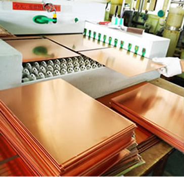
First of all, we need to understand there’re two major parts of SinkPAD board: Top trace layer and copper core/substrate. Then you can see basic manufacturing process of SinkPAD board bellowing: |
|
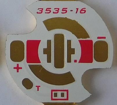
1) Prepare the manufacturing files.On one layer, there’s only trace but without center heatsink PAD of LED and that layer will be named as trace layer; and on another layer, there’re only heatsink PAD, and that layer will be named as copper core layer. >Click For More |

|
2) Produce both trace layer and copper core layer separately.Normally it’s single copper trace layer on that trace layer. But we also have some customers like to design two copper trace layers. That’s also no problem. >Click For More |

|
3) Laminate trace layer and copper core layer together.Also because the electronic related function was on trace layer and thermal conduction was on copper core, they are separated from each other. So that layer also named as Thermoelectric separation circuit board. >Click For More |
|
4) Continue the stripping, solder mask, silkscreen printing and then surface finishing process, like normal FR4 PCB, MCPCB.There’re several basic steps to make soldermask of SinkPAD board: stencil alignment, soldermask printing, board baking, soldermask developing, etching and then soldermask come out. Silkscreen and surface finishing process is the same like other type of circuit board. >Click For More |
|
5) Outline/shape making, electric testing, FQC, shipment, etc. Make the outline using CNC milling, or die-punching.There’re three basic types of outline making of SinkPAD board according to the characteristics of copper core: V-Cutting, CNC routing/milling and Die-punching. V-Cutting will be done firstly and then routing and die-punching. Electronic testing (opening & shorting) will be done after outline. >Click For More |
|
6) Finished the SinkPAD board making.To be noted that the thickness of trace layer with glue is 0.20mm and the depths of copper/thickness of convexity is also 0.20mm, but considering manufacturing process, there’ll be a +/-0.05mm thickness tolerance comparing trace layer and convexity. >Click For More |
|
| Download SinkPAD-Board-Manufacturing-Process-Best-Technology.pdf | |