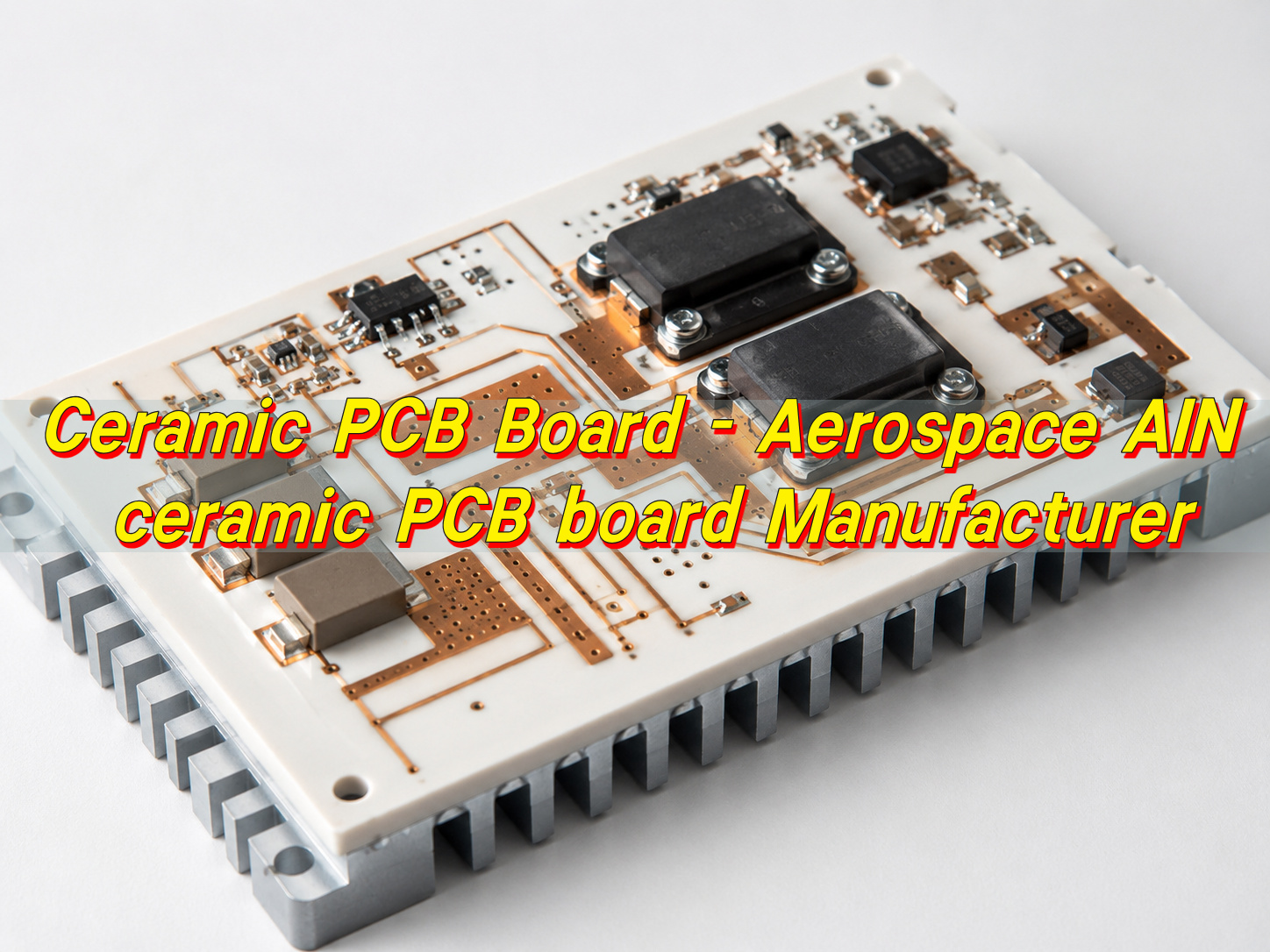
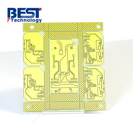
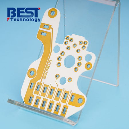
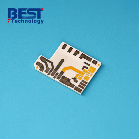
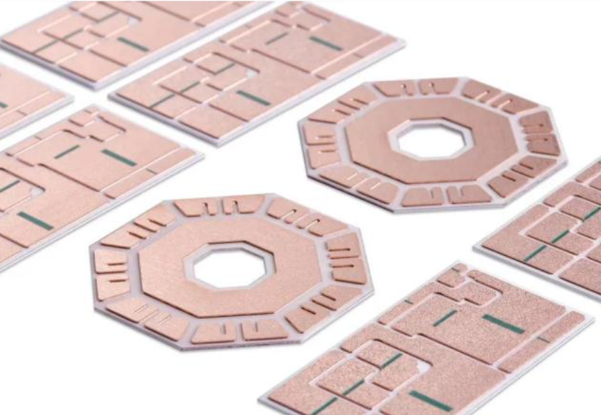
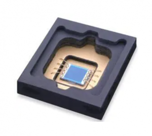
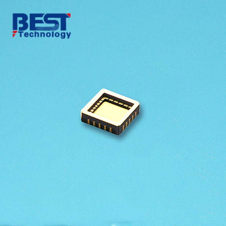
What Is a High Thermal Conductivity Ceramic PCB?
A high thermal conductivity ceramic PCB is a circuit board that uses a ceramic substrate to move heat away from electronic components while maintaining electrical insulation. It is commonly used when FR4, standard metal core PCB, or ordinary thermal interface materials cannot handle the heat density of the design.
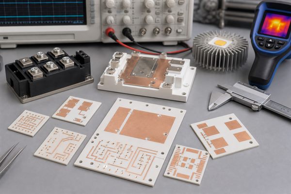
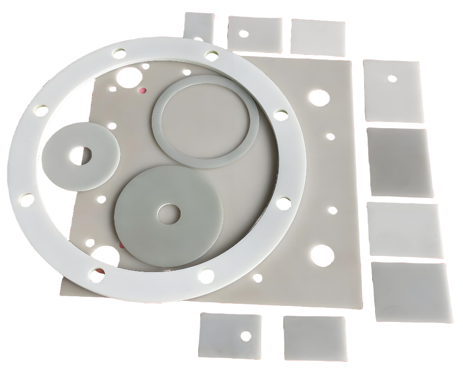
In most engineering discussions, this term refers to ceramic PCB substrates made from materials such as aluminum nitride (AlN), alumina (Al2O3), or in some special cases beryllium oxide (BeO). These materials are selected because they can support circuits and provide a better heat path than many organic PCB materials.
Why Thermal Conductivity Matters in Ceramic PCB Design
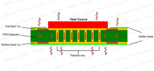
Thermal conductivity matters because high-power components lose performance and reliability when heat stays near the junction, solder joint, or package. A ceramic PCB helps transfer heat from the component into the substrate and then toward a heat sink, housing, or baseplate.
For buyers, the key point is this: higher thermal conductivity is useful only when the whole heat path is designed correctly. Copper thickness, solder area, substrate thickness, mounting pressure, thermal interface material, and heat sink design can all limit real performance. Choosing an expensive ceramic material will not solve the problem if the heat bottleneck is somewhere else.
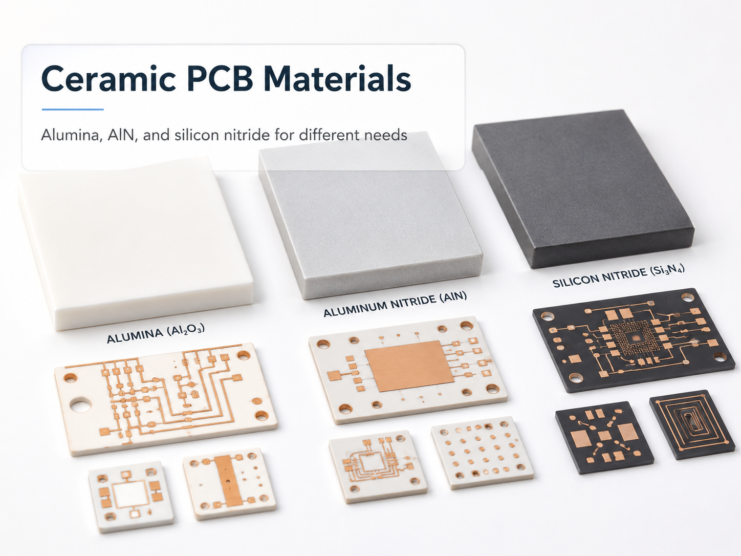
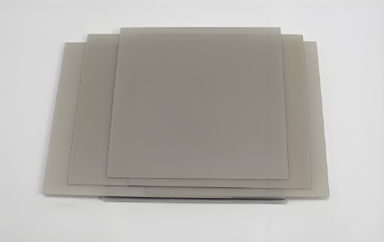
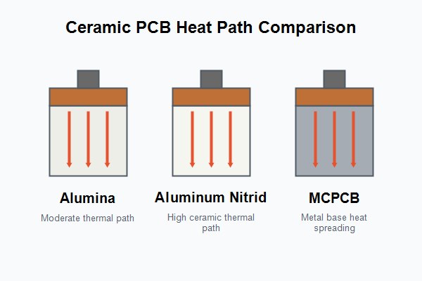
Common Materials for High Thermal Conductivity Ceramic PCBs
The best ceramic PCB material depends on thermal demand, insulation requirement, mechanical reliability, cost target, and application environment.
| Material | Thermal Performance | Strength | Limitation | Best Use |
|---|---|---|---|---|
| Aluminum nitride (AlN) | High | Good thermal performance with electrical insulation | Higher cost than alumina; ceramic handling required | High-power LED, laser, RF, power modules, compact thermal designs |
| Alumina (Al2O3) | Moderate | Cost-effective and widely used | Lower thermal conductivity than AlN | General ceramic circuits, moderate power products, cost-sensitive applications |
| Beryllium oxide (BeO) | High | Strong heat transfer | Safety and handling concerns if dust is generated | Specialized applications with proper safety control |
| Silicon nitride (Si3N4) | Good | Strong mechanical toughness | Cost and availability may vary | Power modules needing mechanical reliability and thermal cycling resistance |
For most PCB and PCBA sourcing projects, AlN ceramic PCB is the common choice when thermal performance is the main priority, while alumina ceramic PCB is often more practical when cost control matters.
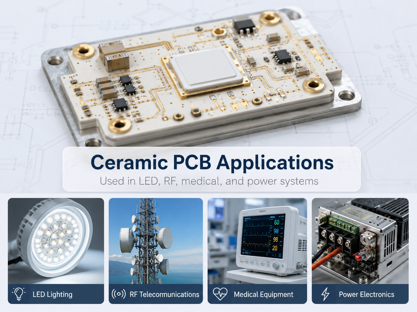
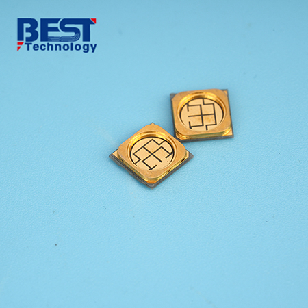
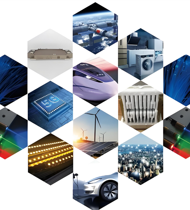
When Should You Use a High Thermal Conductivity Ceramic PCB?
Use a high thermal conductivity ceramic PCB when the product has concentrated heat, limited space, and a real need for electrical insulation. It is most useful when the board itself must become part of the thermal path.
Good use cases include:
- High-power LED modules
- Laser diode submounts
- RF and microwave circuits
- IGBT and MOSFET power modules
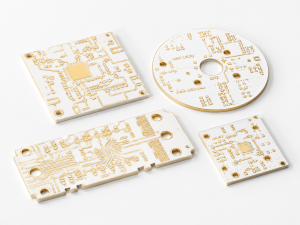
- Automotive power electronics
- Industrial control modules
- Medical electronics with compact power sections
- Aerospace-related electronic modules
- Semiconductor equipment components
A ceramic PCB may be unnecessary if the design has low power, enough board area, loose temperature limits, or can be handled by FR4 with copper pours, vias, heat sinks, or a metal core PCB.
High Thermal Conductivity Ceramic PCB vs Metal Core PCB
The choice between ceramic PCB and metal core PCB depends on whether the design needs stronger insulation, higher thermal stability, or better performance under compact high-power conditions.
| Option | Strength | Limitation | Suitable Application |
|---|---|---|---|
| Metal core PCB | Cost-effective heat spreading for many LED and power designs | Thermal performance depends on dielectric layer; insulation may limit heat transfer | LED lighting, power boards, medium thermal load |
| Ceramic PCB | Good heat transfer with electrical insulation and ceramic stability | Higher cost and stricter manufacturing requirements | High-power density, RF, laser, power module, high-reliability electronics |
The practical takeaway: choose metal core PCB when cost and moderate heat spreading are enough. Choose ceramic PCB when the design needs stronger thermal performance, electrical insulation, and better stability in a compact structure.
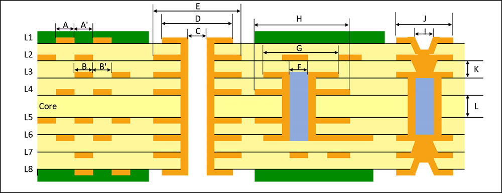
Design Considerations Before Choosing Ceramic PCB
A ceramic PCB should be reviewed as a full thermal and mechanical structure, not only as a substrate material. The board can fail or underperform if copper, solder, component layout, and mounting are not considered together.
Important design points include:
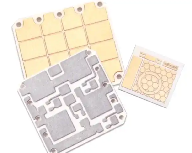
- Substrate material and thickness
- Copper thickness and copper area
- Circuit pattern and isolation distance
- Surface finish and solderability
- Hole design and edge clearance
- Flatness and warpage requirements
- Component heat source location
- Operating voltage and current
- Assembly process and soldering temperature
- Thermal cycling and mechanical stress
- Heat sink or housing contact method
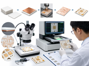
For prototype projects, EBest Circuit (Best Technology) usually needs both electrical files and mechanical information to review whether a ceramic PCB is practical before production.
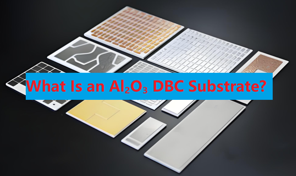
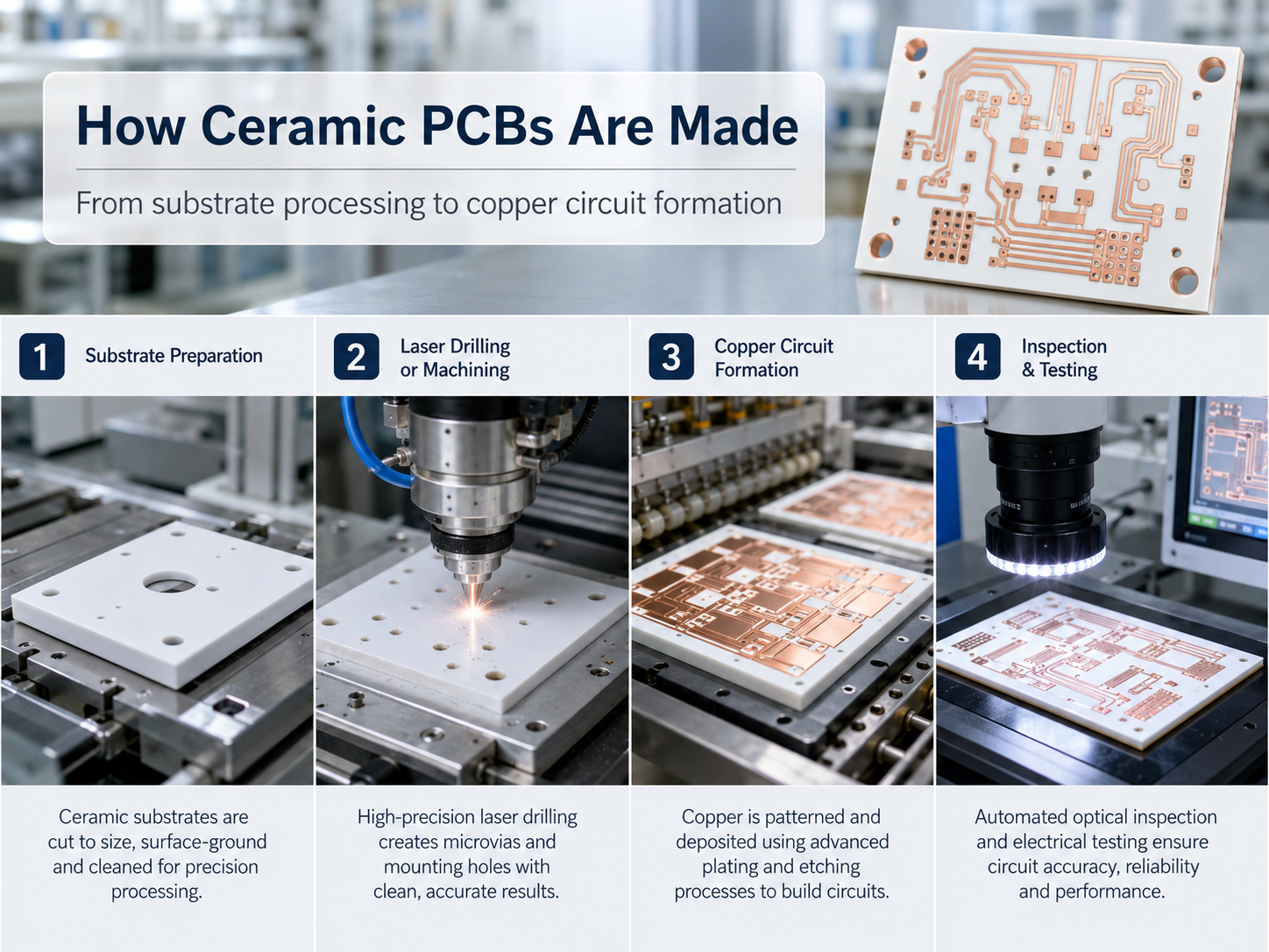
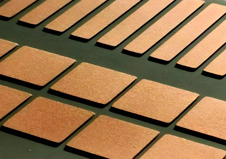
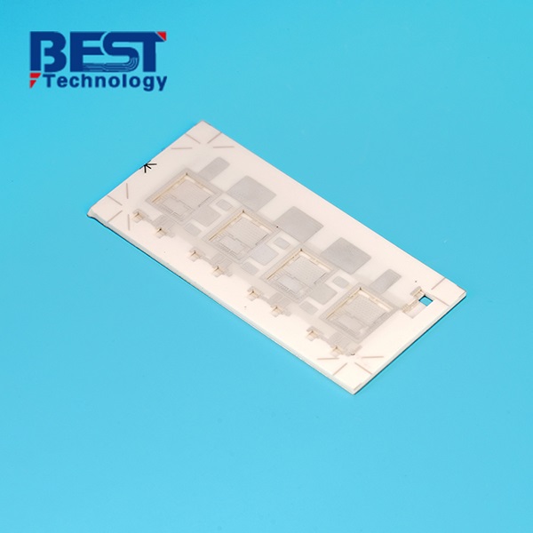
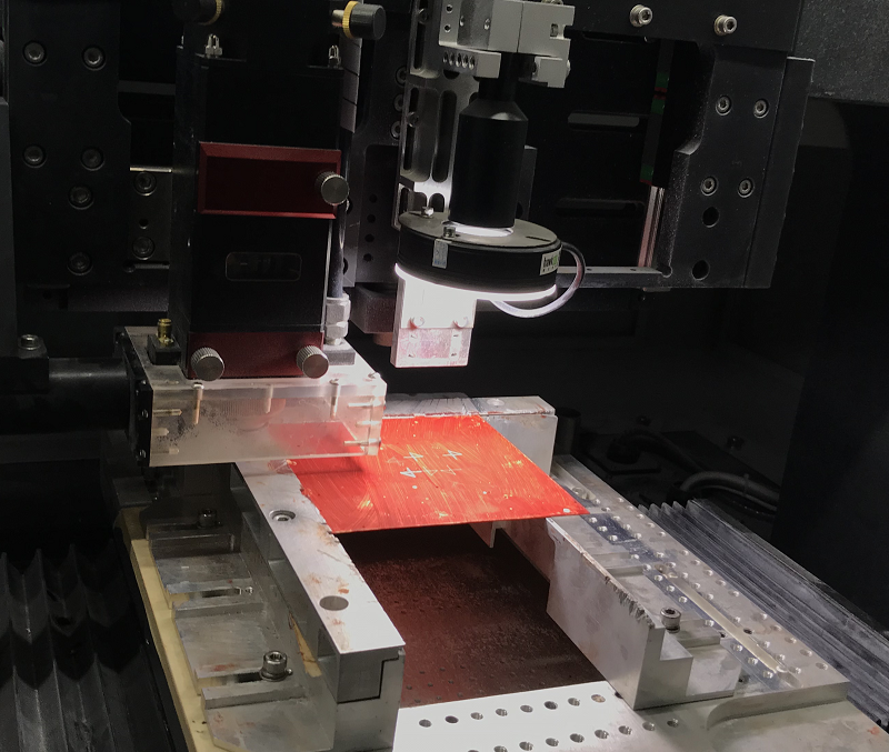
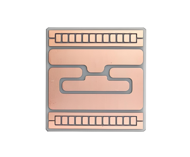
Manufacturing Options for Ceramic PCBs
High thermal conductivity ceramic PCBs can be manufactured using different metallization and bonding methods. The right process depends on circuit complexity, copper thickness, current load, and reliability target.
| Process | Purpose | Suitable For | Buyer Note |
|---|---|---|---|
| Thick film ceramic PCB | Printed conductor paste on ceramic | Hybrid circuits, sensors, simple ceramic circuits | Good for certain functional circuits, but not always ideal for high current |
| Thin film ceramic PCB | Fine metal patterns on ceramic | RF, laser, precision circuits | Suitable when fine lines and stable electrical behavior matter |
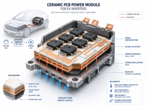
| DBC ceramic substrate | Direct bonded copper on ceramic | Power modules, high-current circuits | Strong option for heavy copper and power electronics |
| AMB ceramic substrate | Active metal brazing copper to ceramic | High-reliability power modules | Often considered when thermal cycling and bonding reliability are critical |
Buyers should not request only “ceramic PCB” in an RFQ. The process type, copper thickness, substrate material, and application requirements should be clear before quotation.
Common Mistakes When Buying Ceramic PCBs
The most common mistake is choosing the highest thermal conductivity material without checking whether the system needs it. This can increase cost without improving final product temperature.
| Mistake | Why It Causes Problems | Better Approach |
|---|---|---|
| Asking only for “high thermal conductivity” | Supplier cannot select the right material or process | Provide heat load, working voltage, substrate size, and copper requirement |
| Choosing AlN for every project | AlN may be unnecessary for moderate thermal loads | Compare alumina, metal core PCB, and AlN based on real temperature target |
| Ignoring copper thickness | Copper affects current carrying and heat spreading | Define copper thickness and current requirements early |
| Missing mechanical constraints | Ceramic can crack under stress or poor mounting | Provide mounting method, pressure, and housing structure |
| No thermal test requirement | Prototype may pass assembly but fail in real operation | Define test temperature, power condition, and acceptance standard |
A reliable ceramic PCB decision should balance thermal performance, electrical insulation, manufacturability, cost, and assembly reliability.
What to Provide When Requesting a Ceramic PCB Quote
A complete RFQ helps the supplier review manufacturability and avoid wrong assumptions. For high thermal conductivity ceramic PCB projects, provide as much application context as possible.
Useful RFQ details include:
- Ceramic material preference, such as AlN or alumina
- Substrate dimensions and thickness
- Copper thickness
- Circuit drawing, Gerber files, or layout files
- Surface finish requirement
- Working voltage and current
- Heat source location and estimated power
- Operating temperature range
- Thermal conductivity target if specified
- Quantity for prototype and mass production
- Assembly requirements if PCBA is needed
- Thermal cycling, insulation, or reliability test requirements
- Approved alternatives or cost target
For EBest Circuit (Best Technology), this information helps the engineering team check whether a ceramic PCB, metal core PCB, or another PCB/PCBA structure is the most practical solution before quotation.
FAQ
What is the best material for a high thermal conductivity ceramic PCB?
Aluminum nitride is often selected when high thermal conductivity is the main requirement. Alumina is more cost-effective for moderate thermal loads. The best choice depends on heat density, voltage isolation, mechanical stress, and budget.
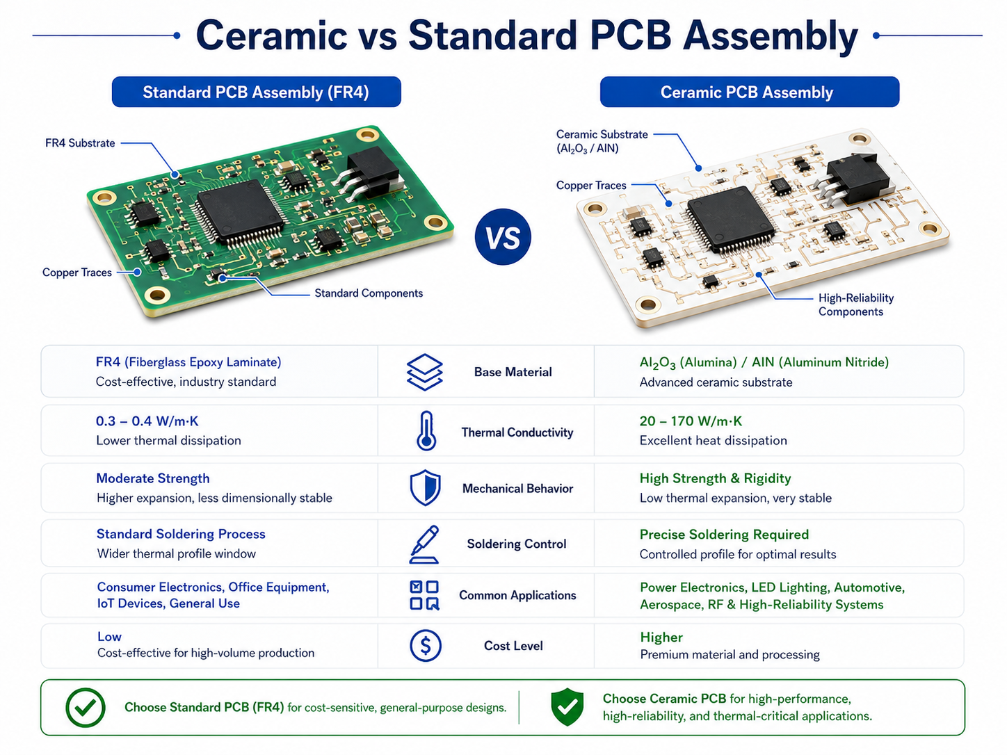
Is ceramic PCB better than FR4?
Ceramic PCB is better than FR4 for high heat density and electrically insulated thermal transfer. FR4 is still better for many standard electronic products because it is lower cost, easier to process, and suitable for normal thermal loads.
Is ceramic PCB better than metal core PCB?
Ceramic PCB can offer better insulation and thermal stability in high-power compact designs. Metal core PCB is usually more cost-effective for LED lighting and moderate thermal applications.
What is an AlN ceramic PCB?
An AlN ceramic PCB uses aluminum nitride as the substrate. It is commonly selected for high-power LED, RF, laser, power module, and other compact electronic designs that need strong heat dissipation.
Does higher thermal conductivity always mean better performance?
No. The full heat path determines real performance. Copper design, solder, interface material, substrate thickness, mounting pressure, and heat sink design can all limit temperature reduction.
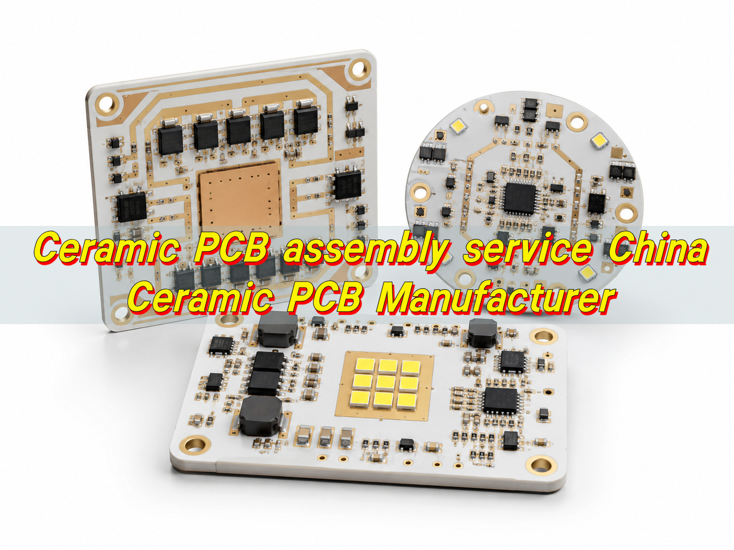
Can ceramic PCB be used for PCBA?
Yes. Ceramic PCB can be assembled with components, but the assembly process should consider soldering temperature, flatness, ceramic handling, component stress, and inspection requirements.
Why is ceramic PCB expensive?
Ceramic PCB is more expensive because ceramic substrate processing, metallization, copper bonding, machining, yield control, and inspection are more demanding than standard FR4 PCB manufacturing.
When is ceramic PCB unnecessary?
Ceramic PCB may be unnecessary when heat is moderate, product cost is sensitive, and FR4, metal core PCB, copper pours, thermal vias, or a better heat sink can meet the temperature target.
Conclusion
A high thermal conductivity ceramic PCB is a strong choice when a product needs heat dissipation, electrical insulation, compact layout, and reliable performance under thermal stress. The right decision depends on material, copper structure, process type, operating conditions, and cost target.
If you are evaluating ceramic PCB, AlN PCB, metal core PCB, or PCBA options for a thermal design, EBest Circuit (Best Technology) can help review your drawings, material choice, copper requirements, prototype needs, and quotation details. Contact us at sales@bestpcbs.com.