PCB manufacturing PCB manufacturing
Home > Blog

Solar Panel PCB Board Manufacturer with Turnkey Solutions

October 9th, 2026

A solar panel PCB board manages charging, power conversion, protection, sensing, and communication in solar controllers, inverters, lighting, and monitoring equipment.

This article examines board selection, materials, environmental protection, manufacturing, testing, cost, supplier evaluation, and the prototype-to-production transition.
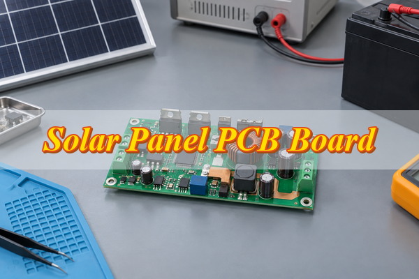
Solar Panel PCB Board, assembled solar control PCB on an engineering workbench

What can make a solar PCB quotation unreliable?

  • You receive quotes for different boards: Charge controllers, inverter boards, lighting controllers, and monitoring boards require different components, copper, assembly processes, and tests.
  • Important costs appear later: Missing voltage, current, battery, cooling, coating, connector, or environmental requirements can change materials, assembly, and testing.
  • The production board differs from the prototype: Unreleased rework, substitutions, firmware, or fixture changes can return as repeat-order problems.

EBest Circuit builds PCBs and PCBAs for solar controllers, inverters, lighting, and monitors. One quotation can cover parts purchasing, fabrication, SMT/THT assembly, firmware programming, and board-level testing.

  • Know what is missing before purchasing: You receive a list of conflicts or open items across the PCB data, BOM, assembly files, mechanics, programming, and tests.
  • Keep one approved build identity: Your BOM, PCB revision, work instructions, firmware, and test limits stay connected throughout production.
  • Repeat the approved result: Accepted substitutions, rework, firmware changes, and test updates are added to the released package for the next order.

Ready for a quotation? Send your current files, quantity, and delivery destination to sales@bestpcbs.com. You will receive a proposed manufacturing scope and a clear list of any information still needed.

What Is a Solar Panel PCB Board?

A solar panel PCB board is the printed circuit assembly inside a solar controller, inverter, light, monitor, or battery-powered product. It carries the components and copper connections used to manage power and system functions.

In a charge controller, the board regulates panel input and battery charging. In an inverter, it supports switching, sensing, protection, and communication. In solar lighting, it can manage charging, LED output, timing, and motion sensing.

The photovoltaic panel generates DC power. The PCB receives, converts, measures, or controls that power inside the equipment. State the equipment and board function in the RFQ so the manufacturer can quote the correct construction, components, assembly process, and tests.

What Types of PCB Boards Are Used in Solar Panel Systems?

Solar systems commonly use charge-control, inverter power, lighting-control, and monitoring or communication boards. Larger products may divide these functions across several PCBAs.

Board Type Main Function Typical Equipment Fit
Charge-control board Regulates panel input, battery charging, load control, sensing, and protection MPPT or PWM controllers, battery chargers, off-grid power units
Inverter power board Converts variable DC power into controlled AC power and manages switching, sensing, and protection Solar inverter PCB assemblies, microinverters, and power-conversion units
Lighting-control board Charges a battery and controls LEDs, timers, dimming, motion sensing, or dusk-to-dawn operation Solar streetlights, garden lights, signs, and remote lighting products
Monitoring or communication board Measures voltage, current, temperature, and status while transferring data to a local or remote system Combiner monitoring, trackers, gateways, remote sensors, and energy-management equipment

How Do You Choose a Solar Panel PCB Board for Your Application?

Match the board to the equipment specification. Start with maximum panel input, battery system, continuous and peak current, required controls, connector interfaces, cooling, and the mounting envelope.

  • Input and battery limits: State normal and maximum panel voltage, battery chemistry, nominal battery voltage, charging method, reverse-polarity behavior, and expected fault conditions.
  • Load and conversion task: Define continuous current, peak or inrush current, output type, switching frequency where relevant, duty cycle, and allowed temperature rise.
  • Control and communication: List sensing accuracy, protection logic, firmware ownership, programming interface, CAN, RS-485, Ethernet, wireless, or other required connections.
  • Mechanical fit: Provide board outline, mounting holes, connector positions, cable direction, height limits, heatsink or chassis contact, and keep-out areas.
  • Operating environment: Identify ambient temperature, humidity, condensation, dust, vibration, enclosure sealing, cleaning, and coating requirements.

Use an off-the-shelf module when its electrical limits, interfaces, dimensions, compliance evidence, and lifecycle fit the product. Use custom manufacturing for unique mechanics or functions, controlled parts and tests, owned design data, and repeat orders.

Which PCB Materials Are Suitable for Solar Electronics?

Use standard FR4 when the board’s temperature, electrical stress, current density, insulation, and assembly requirements stay within its limits. It is a practical choice for many charge-control, lighting, and monitoring boards.

Choose high-Tg FR4 when the expected board temperature or assembly profile needs more thermal margin. Confirm the actual laminate grade and Tg in the quotation instead of accepting a generic “high-temperature material” description.

Use metal-core, ceramic, or heavy-copper construction only when the power or heat path requires it. Ask the manufacturer to confirm routing, isolation, soldering, inspection, cost, laminate, copper, layers, holes, and finish before approval.

How Can Solar Panel PCB Boards Handle Heat and Outdoor Exposure?

Provide the expected current, component losses, maximum ambient temperature, and available cooling. The manufacturer can then check copper areas, thermal vias, interface materials, heatsink or chassis contact, and airflow against your operating conditions.

For outdoor use, state the expected condensation, humidity, dust, salt, UV, and temperature cycling. Specify enclosure and connector protection, spacing, drainage, cleaning, and coating, then verify the prototype under the intended load and environment.

How Are Solar Panel PCB Boards Manufactured and Assembled?

Your approved release should follow the order from file review through fabrication, sourcing, SMT/THT assembly, inspection, programming, and testing. Resolving file conflicts first helps you avoid buying components or tooling against the wrong revision.

  1. Close the file questions: Confirm Gerber or ODB++, drill files, stackup, drawings, netlist, BOM, placement data, polarity, mechanics, quantities, and test requirements.
  2. Fabricate the approved PCB: Build the specified stackup, holes, copper, solder mask, surface finish, and profile, then complete electrical and dimensional checks.
  3. Prepare approved parts and firmware: Verify manufacturer part numbers, allowed alternates, moisture handling, firmware, and programming instructions before kitting.
  4. Assemble and inspect the PCBA: Place and solder SMT and THT parts, then inspect polarity, placement, joints, cleanliness, and mechanical support.
  5. Receive a revision-linked build record: Keep programming, test results, rework, substitutions, inspection findings, and disposition tied to the board you ordered.

Use the prototype build to confirm the soldering sequence, support for heavy magnetics and connectors, manual operations, and inspection access. Approved findings can then become part of the repeat-production instructions.
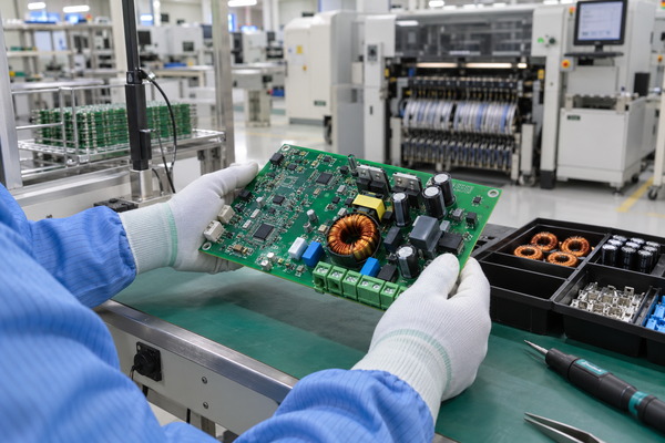
Solar Panel PCB Board, mixed SMT and through-hole assembly inspection for a solar power PCBA

What Tests Should a Solar Panel PCB Board Pass?

Your test plan should show what each check proves and what result you will receive. Specify bare-board electrical test, assembly inspection, firmware programming, functional checks, fixtures, loads, pass limits, and the required record.

  • Charge-control board: Check programmed identity, power-up current, input and output behavior, battery-interface logic, sensing, communications, and agreed protection responses using approved limits.
  • Inverter power board: Add insulation-related checks, gate-drive verification, current and voltage sensing, controlled-load operation, temperature observations, and protection tests appropriate to the design.
  • Monitoring board: Focus on sensor accuracy, analog stability, interface protection, communication, firmware version, low-power behavior, and data integrity.
  • Assembly workmanship: Use visual inspection or AOI for visible joints and placement; apply X-ray only where hidden joints or the risk profile justify it.

Use the board-level results to confirm that the PCBA is ready for product integration. Complete-system validation still needs your actual panel, battery, enclosure, wiring, cooling, firmware, EMC and safety requirements, and intended operating environment.
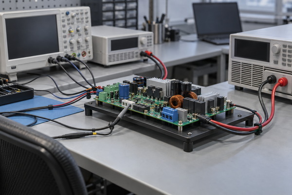
Solar Panel PCB Board, controlled board-level functional testing on a solar electronics PCBA

How Much Does a Custom Solar Panel PCB Board Cost?

Compare quotations only when they cover the same revision, quantity, component responsibility, test coverage, and delivery terms. Otherwise, the lowest price may represent a smaller manufacturing scope.

PCB cost follows size, panel use, layers, laminate, copper, drilling, line and space, finish, tolerances, inspection, and quantity. PCBA adds components, sourcing risk, tooling, placement, SMT/THT work, programming, coating, fixtures, testing, packaging, and specified reports.

Ask for separate one-time, bare-board, component, assembly, programming, testing, packaging, and freight charges. You can then see which costs recur, which items are optional, and which supplier has omitted work you still need.

How Do You Choose a Solar Panel PCB Board Manufacturer?

Choose the manufacturer that gives you the clearest control over cost, revisions, quality, and delivery. Send each supplier the same files and compare the answers and evidence returned with the quotation.

  • A quote matched to your files: Look for confirmation of the stackup, copper, spacing, drill, finish, tolerances, panel conditions, and any special processes that affect price or lead time.
  • One plan for mixed assembly: Confirm how the supplier will handle SMT, THT, selective or manual soldering, heavy parts, connectors, cleaning, coating, and mechanical support.
  • No substitution without your approval: Require manufacturer part numbers, alternate-part rules, and written approval before a material or component change enters the build.
  • Test coverage you can verify: Agree on electrical test, inspection, programming, fixture ownership, functional limits, result format, and the boundary between PCBA testing and system validation.
  • Records you can retrieve: Put the required lot, panel, or serial-number level in your PCB assembly traceability requirements, together with the material, process, firmware, test, rework, and shipment fields you need.
  • A delivery date with clear dependencies: Separate material lead time, fabrication, assembly, testing, approval, shipping, and Incoterm so you know what can change the schedule.

Why Choose EBest Circuit for Solar Panel PCB Board Manufacturing?

Working with EBest Circuit can reduce the handoffs between purchasing, PCB fabrication, assembly, programming, and testing. You send one controlled package and receive one quoted scope for the work EBest will perform.

  • Fewer quotation surprises: A combined file review exposes conflicts among fabrication data, assembly files, parts, mechanics, programming, and tests before materials are committed.
  • More control over component changes: Purchasing follows your approved part numbers and alternate rules, with proposed substitutions sent back for approval when product performance or fit could change.
  • Fewer revision mismatches: PCB construction, BOM, packages, polarity, firmware, and SMT/THT instructions remain tied to the same released build.
  • A smoother move beyond the prototype: Approved rework, part changes, firmware, fixture updates, and test limits can be added to the package before pilot or repeat production.
  • Clear test responsibility: The quotation can state the included inspections, programming, functional checks, customer inputs, fixtures, limits, and result format.
  • Traceability that fits your order: You can define the material, production, firmware, inspection, test, rework, and shipment records you need, plus how they should be retrieved.

You can review the included work, customer-supplied inputs, open decisions, and exclusions before placing the order. This gives your engineering and purchasing teams a common basis for approving cost, schedule, and responsibility.

What Files Are Required for a Custom Solar Panel PCB Board Quote?

You can request a quotation before every detail is final. Send the latest files you have, mark open items clearly, and EBest can return the missing information that affects price, lead time, or manufacturability.

  • PCB files: Gerber or ODB++, drill files, stackup or fabrication drawing, board outline, material, copper, thickness, finish, and quantity.
  • Assembly files: BOM with manufacturer part numbers, pick-and-place data, assembly drawings, polarity notes, and any customer-supplied parts.
  • Programming and test: Firmware and programming instructions, plus the test method, fixture information, operating conditions, limits, and required result format.
  • Order details: Prototype or production quantity, mechanical or coating requirements, delivery destination, required date, packaging, labeling, and traceability needs.

FAQs About Solar Panel PCB Boards

Q1: Can one PCB design support both 12 V and 24 V battery products?

A1: Only when the input range, charging method, component ratings, sensing scale, protection thresholds, thermal behavior, and firmware are designed and validated for both systems. Do not treat a voltage-label change as proof of compatibility.

Q2: Can one PCB revision be assembled with several firmware variants?

A2: Yes, if each variant has a controlled firmware identifier, programming instruction, configuration record, label, and test profile. The finished board must remain traceable to the exact software loaded.

Q3: Is a physical sample enough to reproduce an existing solar control board?

A3: A sample can support inspection, but it rarely defines internal copper, materials, tolerances, approved components, firmware, or test limits. Repeat production should use controlled design and manufacturing data.

Q4: Which changes require another prototype build?

A4: Rebuild and revalidate when a change can affect power conversion, protection, thermal behavior, isolation, component fit, firmware interaction, mechanical integration, or test coverage. Documentation-only corrections may not require a new build.

Q5: How should returned boards be prepared for failure analysis?

A5: Record the board identity, operating conditions, symptoms, event history, firmware, photos, and any work already performed. Avoid cleaning, reworking, or powering the board again unless the analysis plan calls for it.

Q6: Can spare boards be included with a production order?

A6: Yes, but define whether they are finished assemblies, unprogrammed units, or bare PCBs and how they will be packaged, labeled, stored, and tested. Spare units should remain tied to the same approved revision.

Conclusion

A clear solar panel PCB board package gives you comparable prices, visible responsibilities, and a smoother production transfer. Define the function, operating conditions, materials, assembly, tests, quantity, and delivery requirements before approving the supplier.

Send your current Gerber or ODB++, stackup, BOM, assembly data, quantity, test needs, and delivery destination to sales@bestpcbs.com. EBest Circuit will return a proposed turnkey scope and the questions needed to complete your quotation.
You may also like

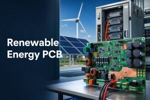
Renewable Energy PCB Manufacturing for Power Equipment

September 3rd, 2026

A renewable energy PCB must keep power conversion, control, protection and monitoring functions stable throughout long operating cycles. For an equipment manufacturer, that means fewer field interruptions, more predictable approvals and a smoother move from prototype to repeat production.

The result depends on more than selecting a PCB material. Current load, voltage spacing, heat, component availability, environmental exposure, assembly processes and testing must be reviewed as one manufacturing system. EBest Circuit (Best Technology) combines DFM review, PCB fabrication, component sourcing, PCBA assembly and customer-defined testing support, giving engineers one team with which to resolve manufacturing questions before they affect delivery.

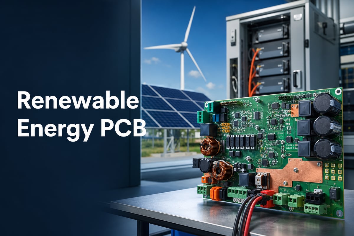
renewable energy PCB
Renewable energy PCB manufacturing for reliable power equipment.

What PCB Requirements Matter Most in Renewable Energy Equipment?

Renewable energy equipment often runs for long periods while switching, converting, storing or measuring power. The PCB requirements should therefore be defined around the board’s actual electrical and operating conditions—not around a generic “industrial PCB” specification.

Key inputs include:

  • Maximum continuous and peak current.
  • Working voltage, transient voltage and isolation requirements.
  • Acceptable conductor and component temperature rise.
  • Ambient temperature, humidity, condensation and contamination exposure.
  • Mechanical loads from connectors, transformers, inductors and installation.
  • Required operating life and repeat-production volume.
  • Inspection, electrical-test and functional-test requirements.

The quotation package should connect these requirements to the Gerber or ODB++ data, stack-up, fabrication notes, BOM, pick-and-place data, assembly drawings and test instructions. This gives the manufacturer enough information to identify conflicts before material is released.

Where Are PCBs Used in Renewable Energy Systems?

A PCB for renewable energy systems may perform power, control, sensing, communication or protection functions. Typical applications include:

  • Solar inverter control and interface boards.
  • Battery energy storage and battery-management assemblies.
  • Wind-turbine control and monitoring electronics.
  • Smart-grid communication and metering equipment.
  • Charging, conversion and power-distribution modules.
  • Energy monitoring, data acquisition and remote-control devices.

These applications do not all need the same board construction. A low-power communications board and a high-current conversion board can sit in the same product but require different copper, spacing, thermal and assembly decisions. Defining the board’s function first prevents an unnecessarily expensive specification—or one that is inadequate for the equipment.

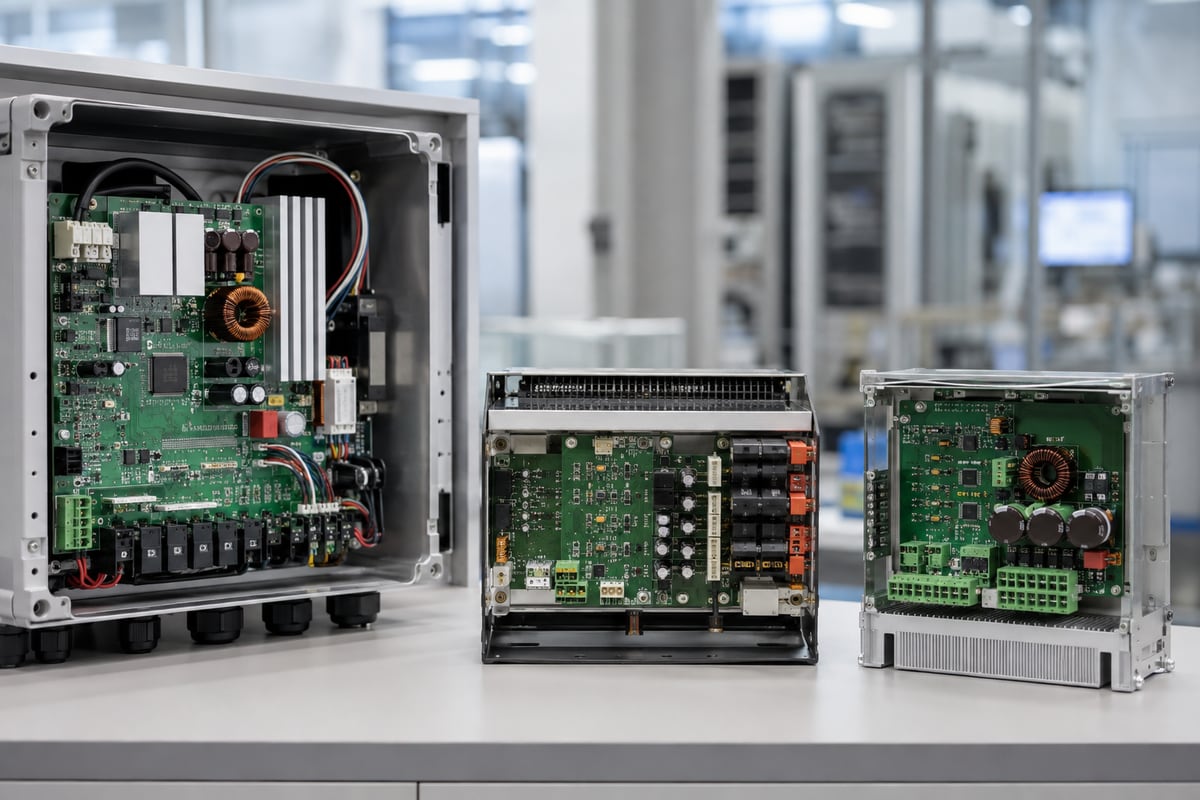
renewable energy PCB
PCB assemblies used in renewable energy power and control equipment.

How Should a Renewable Energy PCB Handle High Current and High Voltage?

Current and voltage requirements affect different parts of the PCB and should be reviewed separately.

For current-carrying paths, engineers should confirm copper weight, conductor width, allowable temperature rise, via current capacity and connector ratings. Heavy copper may be appropriate for some power paths, but it is not automatically required across the entire board. Selective copper construction, wider conductors or a revised layer arrangement may provide a more manufacturable solution. EBest can review the released PCB data for manufacturability, while the customer retains responsibility for the electrical design and current calculations.

For high-voltage areas, creepage, clearance, isolation slots, exposed copper and material properties must match the equipment’s working environment and applicable standards. The high-voltage PCB review should also include solder-mask clearances, component bodies, assembly tolerances and possible contamination—not only nominal spacing in the layout.

Keeping power and control areas clearly defined also makes fabrication inspection and assembly verification more effective.

Which PCB Materials and Stackups Are Suitable for Renewable Energy Systems?

Material selection should follow the electrical, thermal, mechanical and environmental demands of the board.

  • Standard FR-4 can support many control, monitoring and communication boards when its temperature and insulation properties meet the specification.
  • High-Tg FR-4 can provide additional margin for elevated process or operating temperatures.
  • Heavy-copper constructions can support higher-current paths when verified against layout and thermal requirements.
  • Metal-core materials may help selected heat-generating applications, but they have different routing, isolation and assembly constraints.
  • Multilayer constructions can separate power, control and communication functions while supporting controlled return paths and power distribution.

The stack-up should identify material family, finished thickness, copper weights, dielectric requirements and impedance requirements where applicable. Before production, EBest reviews the build against available materials and fabrication capability. Any proposed adjustment should be returned to the customer for approval rather than introduced as an undocumented substitution.

How Is Thermal Management Controlled in Renewable Energy PCBs?

Thermal control begins by understanding where heat is generated and how it can leave the assembly. In an inverter, charger or storage-control product, localized heating may come from power semiconductors, resistors, magnetic components, connectors or high-current copper paths.

Useful controls can include:

  • Wider copper areas and internal or external copper planes.
  • Thermal vias beneath or around heat-generating components.
  • Component spacing that reduces concentrated hotspots.
  • Copper balancing that supports both heat spreading and board manufacturability.
  • Mechanical interfaces to heat sinks, housings or thermal materials defined by the customer.
  • Temperature-rise or functional testing under agreed conditions.

These measures must be evaluated together. Adding copper or thermal vias can change soldering behaviour, board flatness and assembly heat demand. A DFM review helps reveal those manufacturing effects before the first build. For projects that need substantial conductor capacity, the heavy-copper PCB requirements should be confirmed early.

How Can Renewable Energy PCBs Withstand Harsh Operating Environments?

Outdoor cabinets, wind installations, solar equipment and energy-storage systems may expose electronics to humidity, condensation, dust, vibration, corrosive contaminants and repeated temperature changes. The appropriate protection depends on the enclosure and the board’s actual exposure.

Customers should define:

  • Operating and storage temperature ranges.
  • Humidity and condensation conditions.
  • Expected dust, salt, chemical or corrosive exposure.
  • Vibration and mechanical-support requirements.
  • Cleaning and ionic-contamination limits.
  • Conformal-coating material, masking and inspection requirements, when coating is specified.

Manufacturing controls may include material traceability, cleanliness requirements, controlled coating application and inspection, suitable component support and defined acceptance criteria. Conformal coating should not be treated as a universal solution: coating type, coverage, keep-out areas, rework rules and compatibility with connectors or test points must be agreed before production.

What Does Renewable Energy PCB Manufacturing Include?

Renewable energy PCB manufacturing should turn approved design data into a controlled, repeatable board—not simply reproduce a Gerber image.

At EBest, the manufacturing review can cover:

  • Gerber or ODB++ completeness and consistency with fabrication notes.
  • Stack-up, material, copper weight and finished-thickness confirmation.
  • DFM findings affecting spacing, annular rings, drills, routing or panel utilization.
  • Impedance, surface finish and special-process requirements where specified.
  • Panelization and tooling information for customer approval when required.
  • In-process inspection, final inspection and bare-board electrical testing.
  • Lot and material traceability according to the agreed documentation level.

The customer receives identified questions before production release, allowing engineering decisions to be closed while changes are still manageable. This is especially valuable when several power, control and interface boards must be delivered for the same equipment build.

What Does Renewable Energy PCB Assembly Require?

Renewable energy PCB assembly brings component sourcing, soldering, mechanical loading and test access into the manufacturing decision.

The BOM should be checked for manufacturer part numbers, lifecycle status, package consistency, approved alternatives and supply risk. EBest can provide a BOM optimization list when sourcing issues or unclear descriptions are found. No component substitution should be made without customer authorization.

Assembly planning may combine SMT, through-hole, selective soldering, wave soldering or manual operations. Large capacitors, connectors, transformers, inductors and power components may need additional attention to polarity, seating, solder fill, mechanical support and process temperature. AOI can verify visible SMT features, while X-ray may be used where hidden joints or package types require it.

By combining PCB fabrication, component procurement and PCBA assembly, EBest reduces handoffs between separate suppliers. One sales contact supported by three engineers helps customers obtain coordinated answers on PCB, component and assembly questions instead of reconciling several disconnected responses.

renewable energy PCB
Engineering review supports coordinated renewable energy PCB manufacturing and assembly.

How Should Renewable Energy PCBs Be Inspected and Tested?

Testing should produce evidence tied to the customer’s acceptance requirements. A long list of equipment names is less useful than a clear explanation of what is inspected, when it is inspected and how results are recorded.

Depending on the project, the control plan may include:

  • Incoming verification for PCBs and critical components.
  • Solder-paste inspection and AOI for applicable SMT processes.
  • X-ray inspection for hidden solder joints when required.
  • Bare-board electrical testing.
  • In-circuit testing when suitable test access and fixtures are available.
  • Programming and functional testing to customer-provided procedures.
  • First-article verification against approved drawings and BOM revisions.
  • Serial-number, lot and test-result traceability at the agreed level.

EBest’s digital workshop can trace material and product batches, production cycles and manufacturing progress within five seconds. Quality systems include ISO 9001, ISO 13485, IATF 16949 and AS9100D. The applicable documentation and test scope should still be agreed for each order, because a certificate does not replace product-specific acceptance criteria.

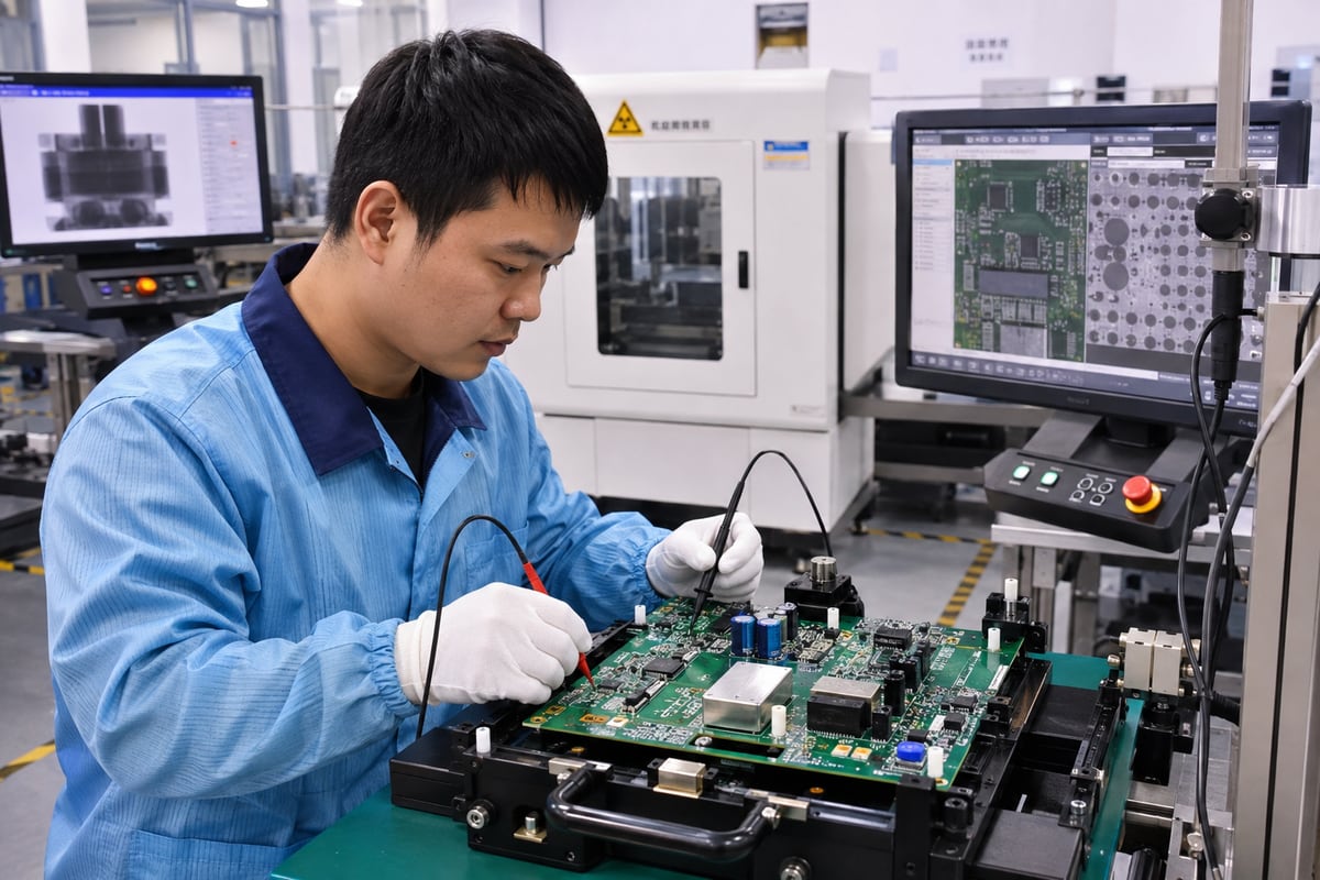
renewable energy PCB
Functional inspection and testing of a renewable energy PCB assembly.

How Do You Move a Renewable Energy PCB From Prototype to Repeat Production?

A successful prototype proves more than basic function when its materials, revisions and test conditions are recorded well enough to support the next build.

Before repeat production, customers and the manufacturing team should close:

  • DFM findings and approved engineering changes.
  • PCB, BOM, firmware and assembly-document revisions.
  • Approved component alternatives and sourcing decisions.
  • Test programs, fixtures and acceptance limits.
  • First-article or golden-sample references where applicable.
  • Packaging, labeling and traceability requirements.
  • Pilot-build results and any corrective actions.

EBest supports samples and low-volume orders so engineering teams can verify the product before scaling. Once the build package is stable, the same controlled data can be used for repeat orders. For suitable PCBA projects with complete, confirmed files and available materials, EBest can support delivery in approximately 1.5 weeks; the confirmed schedule depends on board complexity, component availability, testing and order quantity.

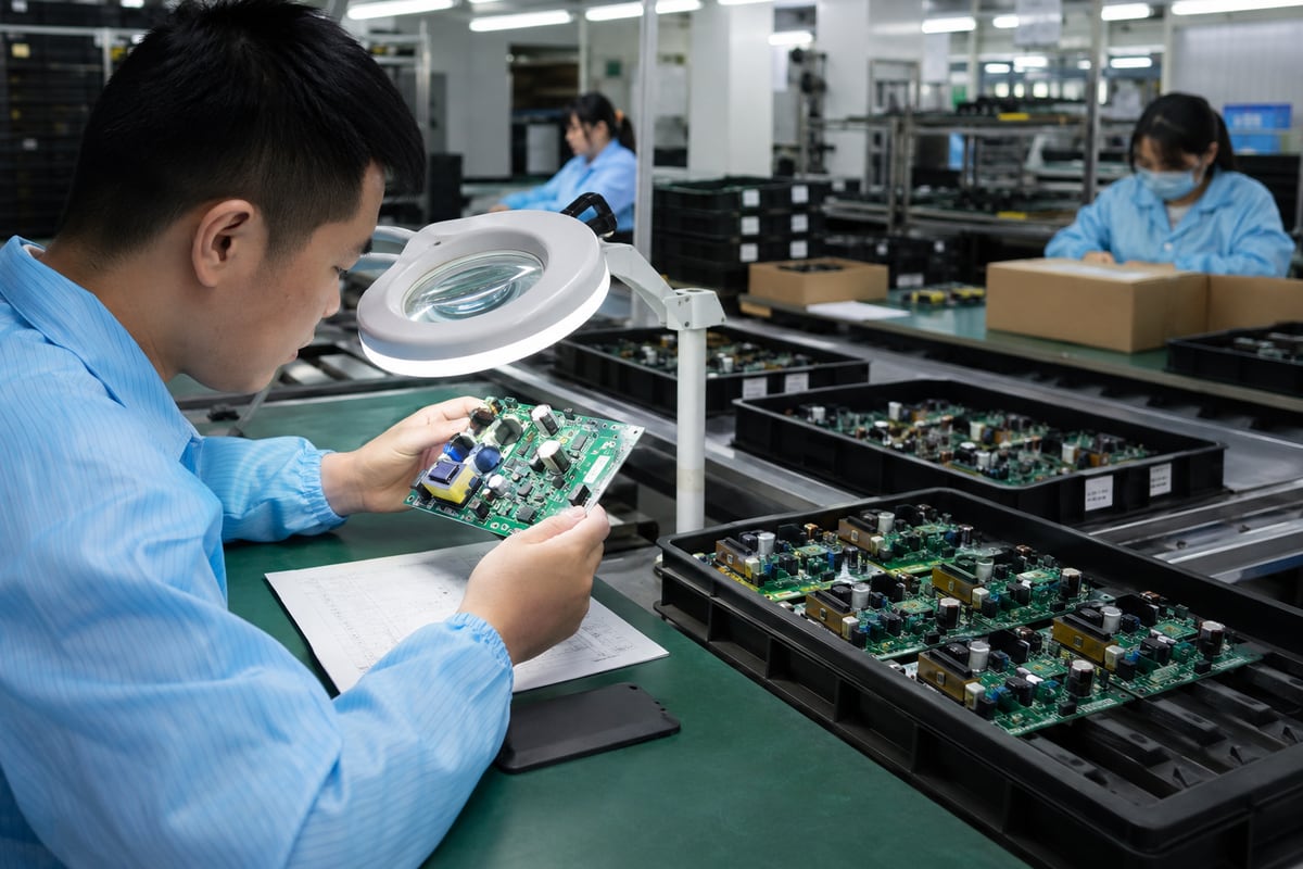
renewable energy PCB
Controlled inspection helps move renewable energy PCB projects into repeat production.

What Should You Check When Choosing a Renewable Energy PCB Manufacturer?

A suitable manufacturer should help you obtain a production result—not merely return the lowest unit price. Before placing an order, check whether the supplier can provide:

  • PCB fabrication and PCBA assembly under coordinated project control.
  • DFM feedback linked to the released design files.
  • BOM review, authorized sourcing and alternative-part control.
  • Relevant high-current, high-voltage, thermal and material capability.
  • Prototype and low-volume support before repeat production.
  • Inspection and customer-defined testing with usable records.
  • Revision, material, batch and product traceability.
  • Quality certifications relevant to your market and project.
  • Clear lead-time assumptions and responsive engineering communication.

EBest has focused on PCB and PCBA manufacturing for 20 years, operates its own PCB and PCBA factories and works with more than 1,000 supply-chain partners. More importantly for a customer, the integrated service means one team can review manufacturability, components, assembly and testing before quoting a delivery plan.

For an accurate review, send the Gerber or ODB++ files, fabrication drawing, stack-up, BOM, pick-and-place data, assembly drawings, expected quantities and test requirements to sales@bestpcbs.com. EBest will review the manufacturing package and identify the information needed to prepare the quotation.

FAQs About Renewable Energy PCB Manufacturing and Assembly

What PCB materials are used in renewable energy equipment?

FR-4 is common for control and monitoring boards. High-Tg FR-4, heavy-copper constructions, metal-core materials or multilayer stack-ups may be considered when temperature, current, insulation or heat-spreading requirements justify them. The correct choice depends on the board’s function and operating environment.

Do renewable energy PCBs always require heavy copper?

No. Heavy copper is useful when the verified current and temperature-rise requirements demand it. Many communication, sensing and control boards can use standard copper weights. The current path, conductor geometry, via structure and cooling conditions should determine the requirement.

What copper thickness is suitable for high-current power equipment?

There is no single suitable value for every product. Current, trace width, layer position, allowable temperature rise, duty cycle and cooling conditions must be considered together. The customer defines the electrical requirement; the manufacturer confirms whether the released construction can be fabricated consistently.

Can one supplier handle both PCB fabrication and assembly?

Yes. EBest provides PCB fabrication, component sourcing and PCBA assembly as an integrated service. This can simplify revision control and reduce the coordination required between separate board, component and assembly suppliers.

What testing is available for renewable energy PCB assemblies?

Available controls can include incoming inspection, AOI, X-ray where required, bare-board electrical testing, ICT and customer-defined functional testing. The final test plan depends on the design, test access, fixtures, software and acceptance criteria supplied for the project.

Can renewable energy PCBs be prototyped before volume production?

Yes. Prototype and low-volume builds allow engineers to verify fit, function, assembly conditions and test coverage before repeat production. Changes should be documented and incorporated into the controlled production files after validation.

What files are needed for a renewable energy PCB quotation?

Send Gerber or ODB++ data, fabrication notes, stack-up requirements, BOM, pick-and-place files, assembly drawings, quantities and testing instructions. Providing complete and revision-matched files helps the engineering team return a more accurate quotation and schedule.

Ready to move your renewable energy electronics from approved files to a controlled build? Send your project package to sales@bestpcbs.com for DFM, PCB fabrication, sourcing, assembly and testing review. EBest will help you establish a practical manufacturing route for your renewable energy PCB.

You may also like

New Energy PCB Manufacturer with One-Stop PCB and PCBA Support

June 11th, 2026

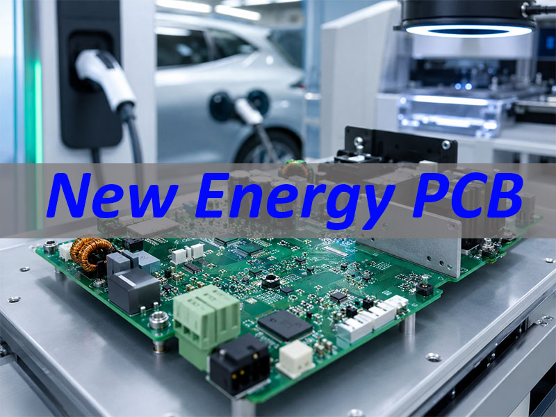
New Energy PCB is used in EVs, chargers, energy storage systems, solar inverters, LED power modules, and power control electronics. This article explains how EBest Circuit (Best Technology) supports New Energy PCB projects with PCB fabrication, material review, PCBA assembly, testing, and engineering communication.

What problems do OEM buyers often face in New Energy PCB projects?

  • Wrong material choice: FR4, high-Tg FR4, aluminum, copper base, ceramic, HDI, or heavy copper may all be possible.
  • Slow prototype review: Missing stack-up, copper thickness, or test notes can delay quotation.
  • Unclear current and heat requirements: High-current areas may need thicker copper or better thermal paths.
  • PCBA handoff risk: PCB, BOM, SMT, DIP, and testing may be handled by separate suppliers.
  • Low-price trap: A cheap quote may ignore manufacturability, testing, or repeat production.

EBEST helps reduce these risks with focused engineering review.

  • Material matching: We review board type, copper thickness, Tg, and thermal needs.
  • Fast file review: We check Gerber files, stack-up, BOM, and assembly drawings early.
  • High-current support: We review copper weight, terminals, connectors, and heat paths.
  • One-stop PCBA: We connect PCB fabrication, sourcing review, SMT, DIP, inspection, and testing.
  • Repeatable production: We review prototype projects with later small-batch and repeat orders in mind.

EBest Circuit (Best Technology) is a PCB and PCBA manufacturer supporting FR4 PCB, high-Tg FR4 PCB, heavy copper PCB, aluminum PCB, copper base PCB, ceramic PCB, HDI PCB, rigid-flex PCB, RF microwave high-frequency PCB, and PCBA assembly. For New Energy PCB projects, please send Gerber files, BOM, stack-up, copper thickness, material notes, assembly drawings, testing requirements, quantity, and delivery target to sales@bestpcbs.com.

New Energy PCB

What Should OEM Buyers Confirm Before Starting a New Energy PCB Project?

Before starting a New Energy PCB project, OEM buyers should confirm the real operating conditions. These details decide the material, copper thickness, thermal structure, assembly method, and testing plan.

ItemWhat to Confirm
ApplicationEV, charger, energy storage, inverter, LED, or power control
Current loadSignal board, power board, or high-current path
Thermal needStandard FR4, aluminum, copper base, ceramic, or other option
PCBA scopeBare PCB only or PCB plus assembly
Testing needElectrical test, functional test, aging, or customer test method

EBEST does not use one PCB type for every new energy project. We review the application first, then match the board structure.

For example, a control board may use high-Tg FR4. A heat-focused board may need aluminum or copper base. A high-current board may need heavy copper. A compact control module may need HDI. A high-power thermal design may need ceramic PCB.

A clear project start helps reduce quotation changes and production delay.

How Can EBEST Speed Up New Energy PCB Prototype Review?

A New Energy PCB prototype should help customers test faster, not create new questions during production. EBEST speeds up prototype review by checking the key files before fabrication.

We usually review:

  • Gerber and drill files
  • Stack-up
  • Board thickness
  • Copper thickness
  • Material grade
  • Surface finish
  • Minimum line width and spacing
  • Minimum hole size
  • High-current areas
  • Connector and terminal zones
  • Test points
  • BOM and assembly drawings if PCBA is needed

For high-Tg FR4 projects, EBEST can review Tg requirements such as standard Tg, Tg 150, or Tg 170–180 options. For high-frequency or communication-related new energy boards, we can review materials such as Rogers, Taconic, Arlon, Nelco, and other specified laminates when required.

For prototype projects, the goal is simple: confirm what can be built, what may affect lead time, and what should be adjusted before mass production.

What Does EBEST Check Before Quoting a New Energy Vehicle PCB?

Before quoting a New Energy Vehicle PCB, EBEST reviews cost-driving and risk-driving details. A useful quote should reflect the real board, not only the size and quantity.

We check:

  • Layer count
  • Board thickness
  • Copper weight
  • Material type
  • Surface finish
  • HDI or blind/buried via structure
  • Heavy copper requirement
  • Impedance requirement
  • Connector and terminal areas
  • Minimum hole size
  • Solder mask bridge
  • Electrical testing
  • PCBA and functional testing needs

EBEST’s process capability covers a wide range of PCB requirements, including multilayer PCB, HDI PCB, heavy copper PCB, aluminum PCB, high-frequency PCB, and thick board projects. For heavy copper designs, line width and spacing must be reviewed together with copper weight. For example, a 1 oz board and a 10 oz or 20 oz heavy copper board cannot use the same fabrication rules.

That is why New Energy Vehicle PCB quotation must start with engineering review.

A low quote without copper, material, and testing review is not a reliable quote.

How Does EBEST Support New Energy Charger PCB Assembly?

New Energy Charger PCB Assembly usually involves power components, connectors, relays, transformers, terminals, heat-generating parts, and test requirements. EBEST reviews the PCB and PCBA together so the project does not fail at the assembly stage.

Our support can include:

  • PCB fabrication
  • BOM review
  • Component sourcing review
  • SMT assembly
  • DIP assembly
  • BGA/QFN assembly when needed
  • Connector and terminal assembly
  • AOI inspection
  • X-ray inspection when required
  • First article inspection
  • Customer-defined functional testing

For charger boards, we focus on high-current paths, spacing, soldering areas, connector strength, thermal zones, and test access. If the PCB design is difficult to assemble, we will raise the issue before production.

This is the value of one-stop PCB and PCBA support: fewer handoffs, clearer responsibility, and better preparation for repeat orders.

Which PCB Technologies Can EBEST Match to New Energy Applications?

New Energy PCB is not one fixed board type. EBEST matches PCB technology based on current, heat, space, reliability, and assembly needs.

PCB TechnologySuitable New Energy Use
FR4 PCBControl boards and signal circuits
High-Tg FR4 PCBHigher thermal resistance
Heavy Copper PCBHigh-current paths and power distribution
Aluminum PCBLED power and heat dissipation
Copper Base PCBHigh thermal transfer power boards
Ceramic PCBHigh-power and high-thermal applications
HDI PCBCompact control modules
High-Frequency PCBCommunication or RF-related modules
Rigid-Flex PCBSpace-limited or vibration-sensitive products

EBEST also supports multiple surface finishes, including HASL, lead-free HASL, ENIG, immersion tin, immersion silver, hard gold, soft gold, ENEPIG, carbon ink, and gold finger plating when required.

This matters because new energy products may need more than standard FR4. A charger, inverter, EV control board, battery system, or LED power board may need different copper, material, surface finish, and assembly plans.

The right PCB technology should support the product, not just meet the drawing.

What Manufacturing Challenges Should New Energy PCB Buyers Watch For?

New Energy PCB projects often fail because small manufacturing details are ignored early.

Common risks include:

  • Copper mismatch
    High-current areas may need thicker copper or wider current paths.
  • Wrong material
    Standard FR4 may not be enough for thermal or reliability needs.
  • Poor thermal path
    Heat may require aluminum, copper base, ceramic, or better copper design.
  • Connector stress
    Terminals, screws, and power connectors may create mechanical risk.
  • Unclear testing
    Electrical test alone may not prove product function.

EBEST reduces these risks through DFM review, material confirmation, process capability review, PCBA planning, inspection, and customer-defined testing.

For new energy projects, “cheap” should not be the main decision. A practical supplier should help control cost while protecting manufacturability and reliability.

The better result is a board that can be built, assembled, tested, and repeated.

New Energy Charger PCB Assembly Case: How Did EBEST Support an OEM Customer?

An OEM customer needed a New Energy Charger PCB Assembly project for a power control board used inside new energy charging equipment. The board had to support power-control signals, connector interfaces, stable impedance performance, and reliable PCBA assembly for later repeat production.

For this project, EBEST focused on five key areas:

  • Application review
    The PCB was used in a new energy charger power control module, so EBEST reviewed the design around signal stability, connector layout, assembly reliability, and production repeatability.
  • Complex PCB structure
    This was a 12-layer FR4 PCB with Tg 170 material, 1 oz inner and outer copper, 4.8 mm board thickness, ENEPIG surface finish, and controlled impedance requirements.
  • Engineering review before production
    EBEST reviewed the Gerber files, BOM, stack-up, copper thickness, impedance notes, assembly drawing, and testing requirements before fabrication and assembly.
  • Manufacturing and assembly control
    The review focused on multilayer stack-up, ENEPIG process control, impedance control, connector reliability, soldering process stability, AOI inspection, first article checking, and customer-defined test support.
  • One-stop project value
    EBEST helped the customer reduce communication gaps between PCB fabrication, BOM review, SMT assembly, DIP connector assembly, inspection, and testing.

Key project parameters:

  • Application: New energy charger power control board
  • PCB type: 12-layer FR4 PCB
  • Material Tg: Tg 170
  • Copper thickness: 1 oz inner and outer copper
  • Board thickness: 4.8 mm ±10%
  • Solder mask / silkscreen: Green solder mask, white silkscreen
  • Surface finish: ENEPIG
  • Nickel thickness: 120 μin–276 μin
  • Palladium thickness: 1 μin–5 μin
  • Gold thickness: 1 μin
  • Impedance: Controlled impedance required
  • PCBA scope: SMT assembly, DIP connector assembly, inspection, and customer-defined test support
  • Project value: PCB fabrication and PCBA assembly were reviewed together to improve manufacturability and repeat production stability.
New Energy PCB

FAQs About New Energy PCB

What Is a New Energy PCB?
A New Energy PCB is a printed circuit board used in EVs, chargers, solar systems, energy storage, inverters, power electronics, LED systems, and related control modules.

Can EBEST Support New Energy PCB Prototype Projects?
Yes. EBEST can review Gerber files, stack-up, copper thickness, material choice, surface finish, BOM, assembly drawings, and test requirements before production.

What PCB Types Are Common in New Energy Projects?
Common options include FR4 PCB, high-Tg FR4 PCB, heavy copper PCB, aluminum PCB, copper base PCB, ceramic PCB, HDI PCB, high-frequency PCB, and rigid-flex PCB.

Can EBEST Provide New Energy Charger PCB Assembly?
Yes. EBEST can support PCB fabrication, component sourcing review, SMT assembly, DIP assembly, inspection, and customer-defined testing for charger PCB projects.

What Files Should I Send for a New Energy PCB Quote?
Please send Gerber files, drill files, stack-up, copper thickness, material notes, BOM, pick-and-place file, assembly drawing, testing requirements, quantity, and delivery target.

All in all, new energy PCB supports EVs, chargers, energy storage, solar systems, inverters, LED power, and other power electronics products. This article explained how EBEST reviews material, copper, prototype files, charger PCBA needs, PCB technologies, manufacturing risks, and one real charger PCBA case.

EBest Circuit (Best Technology) supports New Energy PCB projects with PCB fabrication, PCBA assembly, material review, component sourcing review, SMT, DIP, inspection, testing, and engineering communication. Please send your files and requirements to sales@bestpcbs.com for review.

You may also like