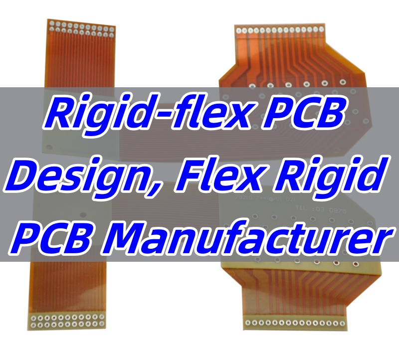
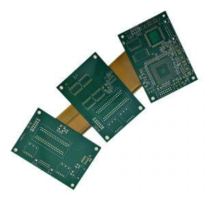
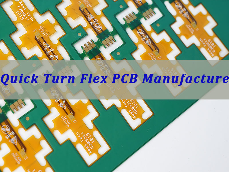
Quick turn flex PCB manufacturer services matter because they help engineers move from design files to validated hardware faster, with fewer process risks and better control over flexible and rigid-flex board performance. This article explains how flex and rigid-flex PCB manufacturing works, what customers should evaluate in a supplier, and why one-stop PCB assembly can reduce both development time and avoidable errors.
What usually frustrates customers when sourcing a quick turn flex PCB manufacturer?
- Lead times slip when design review is weak.
- Flex materials and stack-up choices are unclear.
- Rigid-flex reliability risks appear too late.
- PCB fabrication and assembly are split across vendors.
- Prototype builds do not scale smoothly into small batches.
A capable one-stop supplier solves those problems by aligning design, fabrication, sourcing, and assembly from the start.
- Perform early DFM review before tooling release.
- Recommend fit-for-purpose materials, stack-up, and stiffeners.
- Control critical rigid-flex process steps and bend-zone protection.
- Integrate PCB fabrication, component sourcing, and PCB assembly.
- Support prototype, pilot run, and low-volume production in one flow.
EBest Circuit (Best Technology) is a professional PCB and PCBA manufacturer with strong experience in flex PCB manufacturing, rigid flex PCB manufacturing, component sourcing, and one-stop assembly support. We help engineers shorten development cycles through DFM analysis, process matching advice, prototype support, and fast-response project coordination. For projects that demand speed and technical depth, pls contact us via sales@bestpcbs.com.
How Does The Flex PCB Manufacturing Process Work From Design To Production?
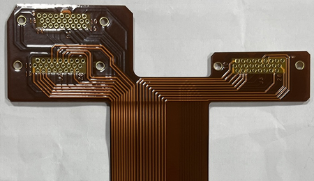
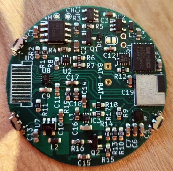
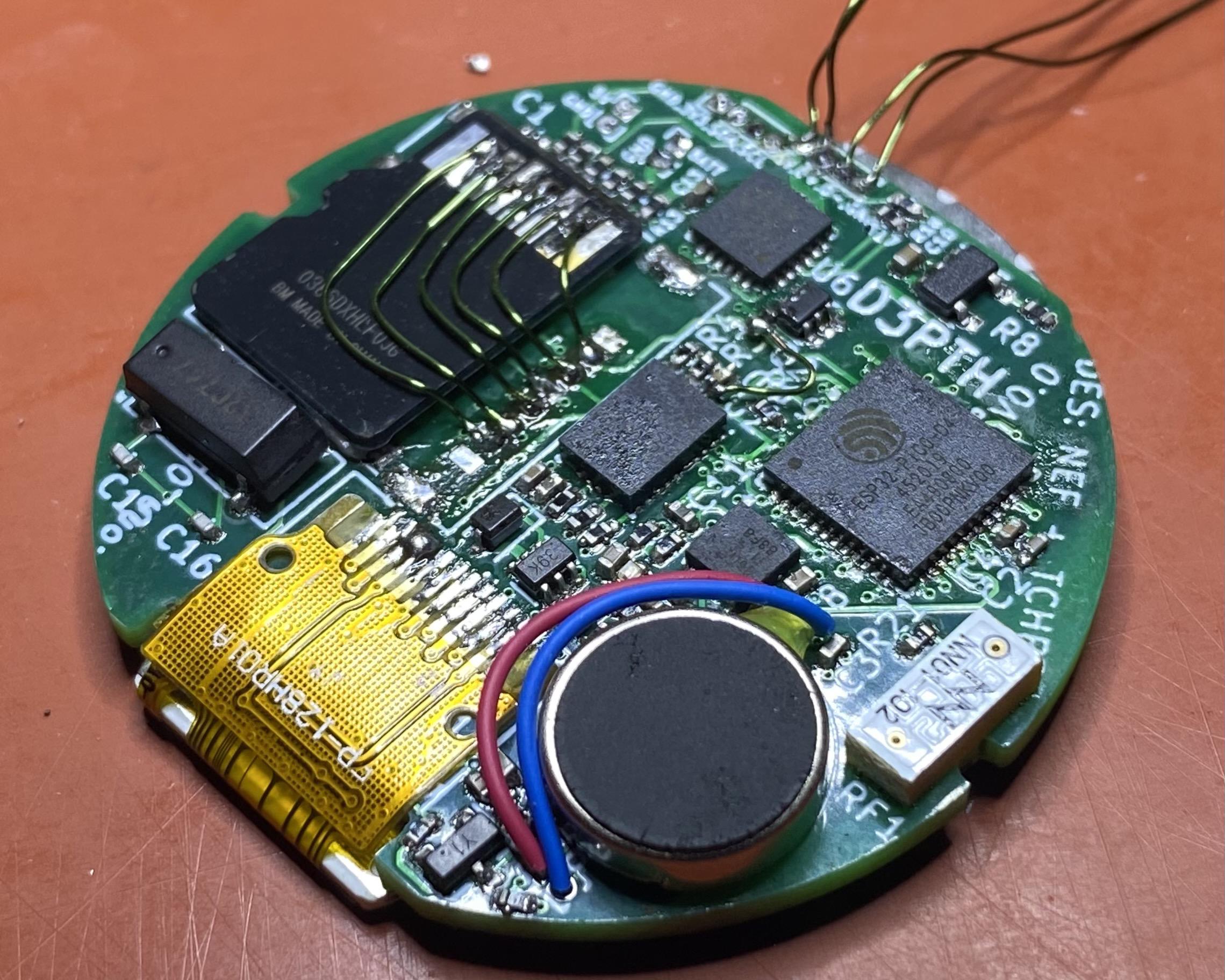
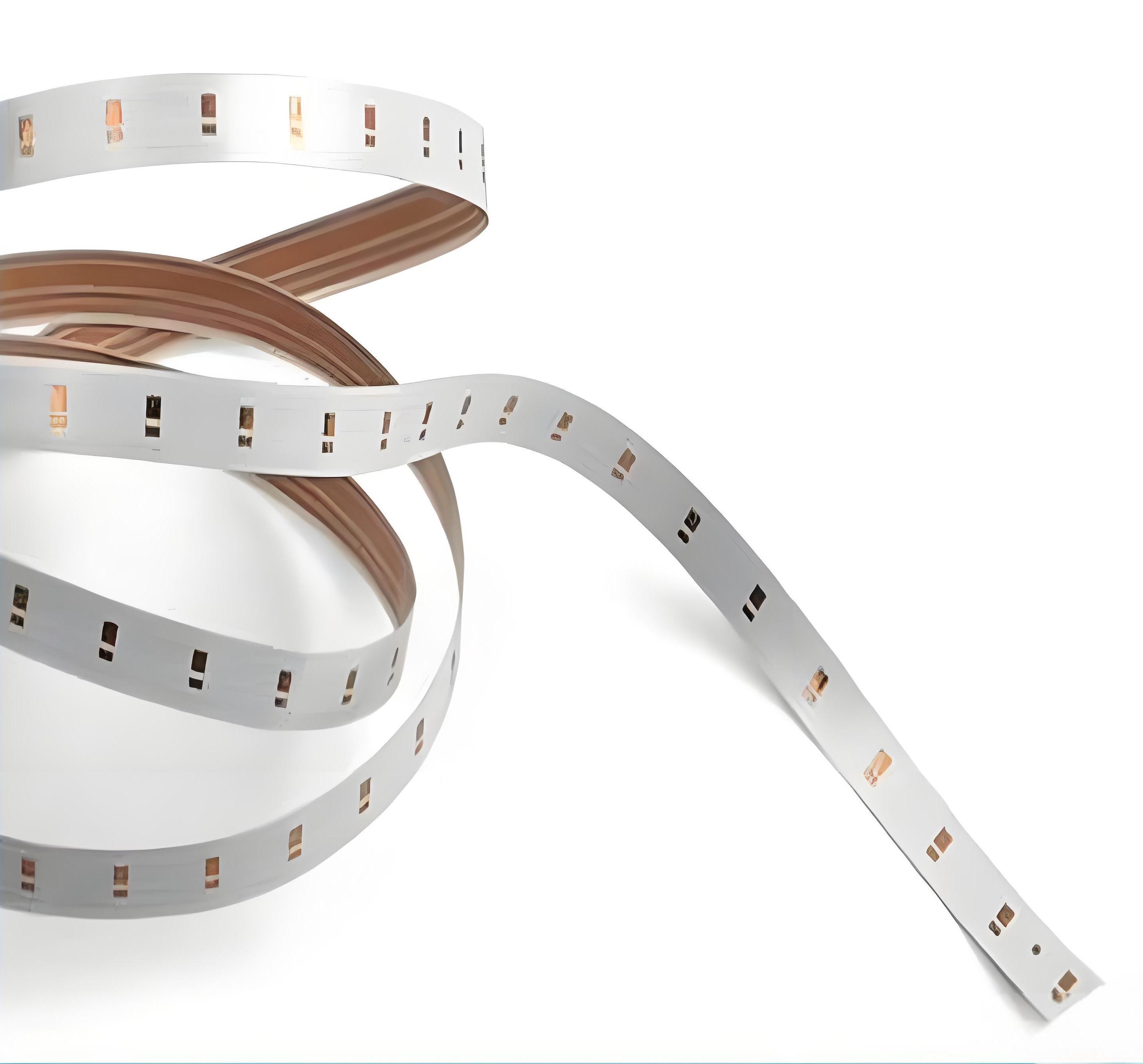
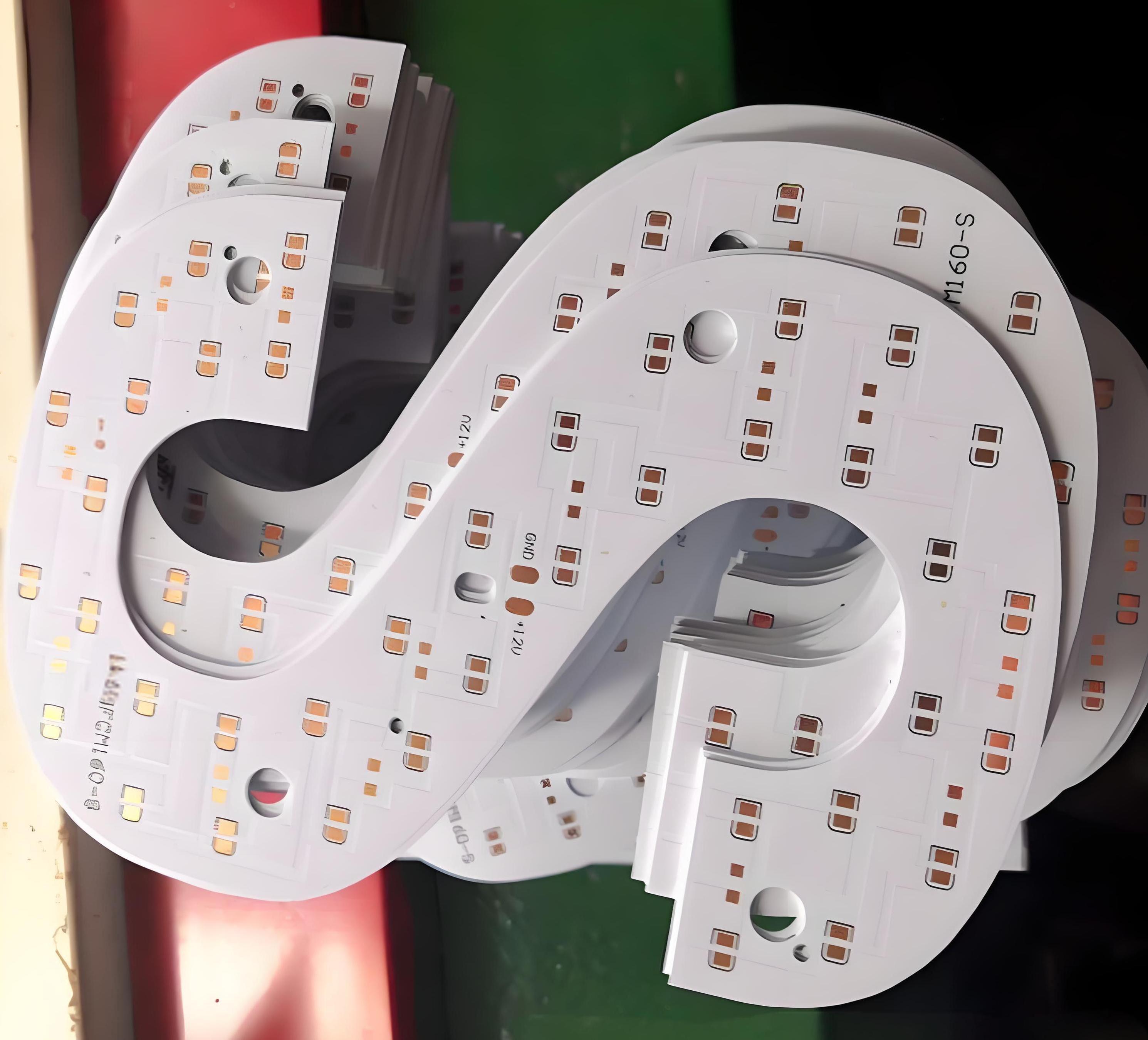
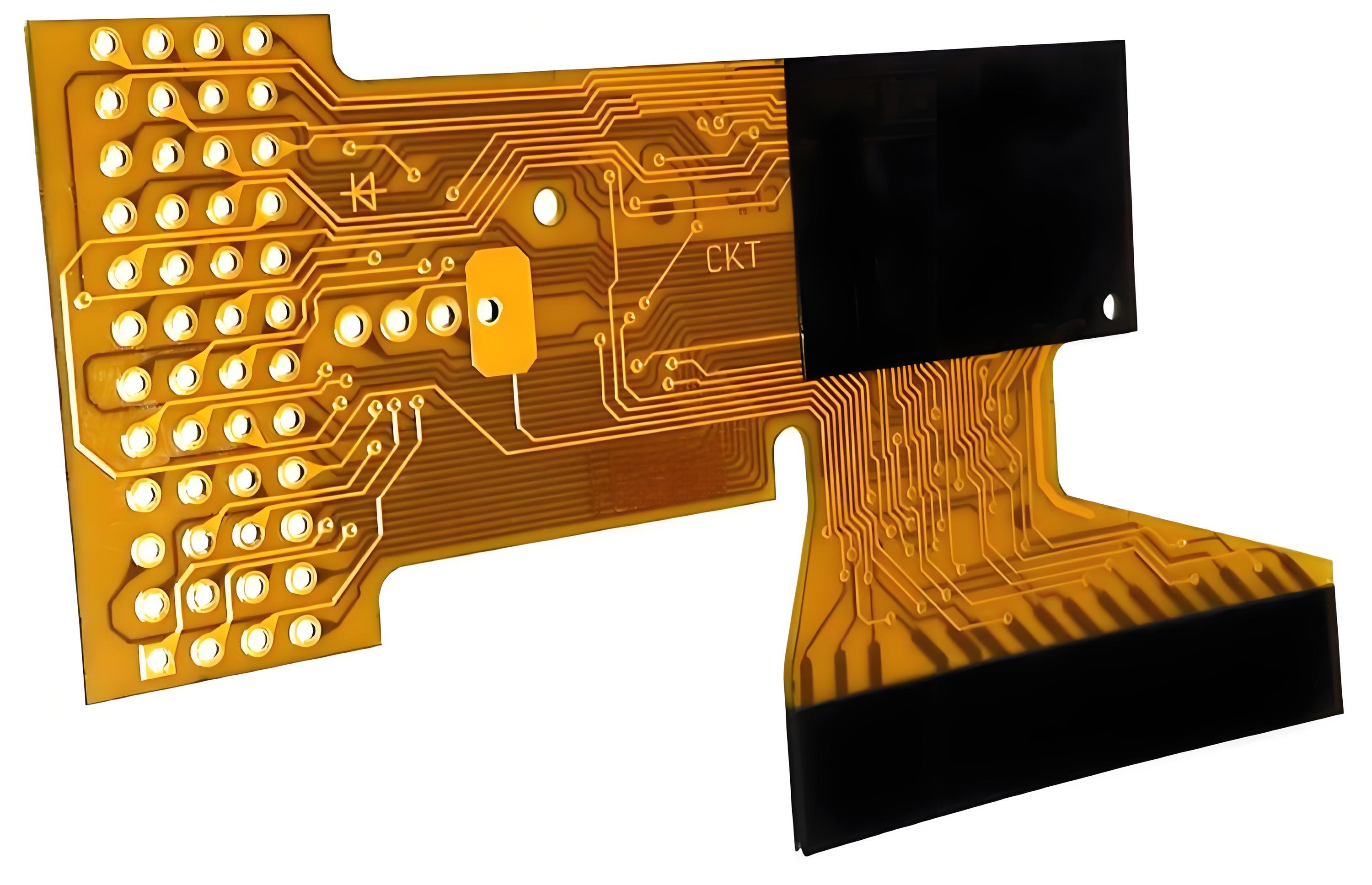
The flex PCB manufacturing process is not just a lighter version of standard PCB production. It is a controlled sequence built around thin base materials, bending performance, dimensional stability, and assembly compatibility. If any one of these is mishandled, the board may pass electrical test but still fail in use.
A practical production flow usually includes the following stages:
- Design Data Review
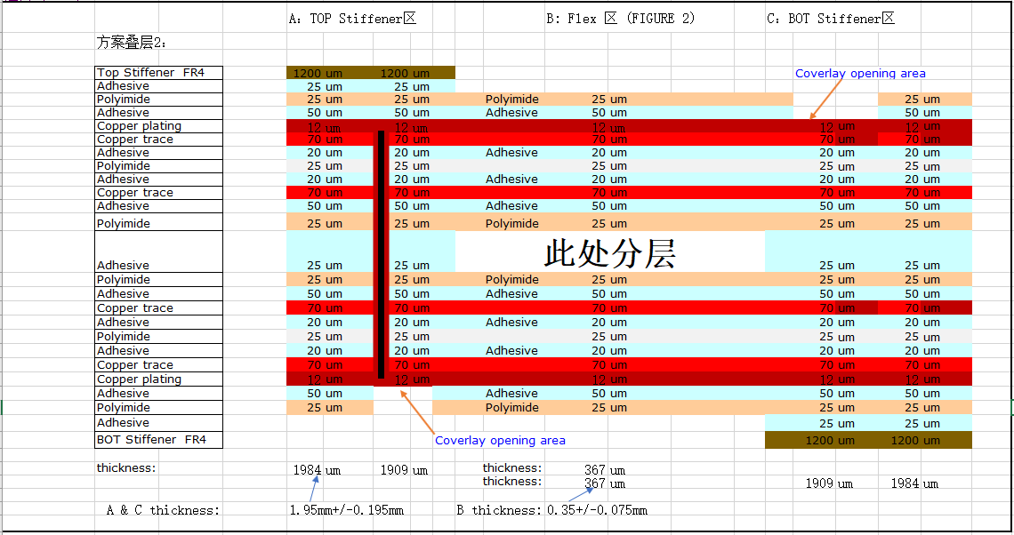
Gerber, stack-up, coverlay openings, stiffener drawings, and bend-zone rules are checked first. This is where many prototype delays can be prevented. - Material Selection
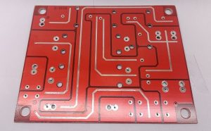
Common flex materials include polyimide base film, rolled annealed copper, adhesive or adhesive-free constructions, coverlay, and stiffener materials such as FR-4, PI, or stainless steel. - Circuit Pattern Formation
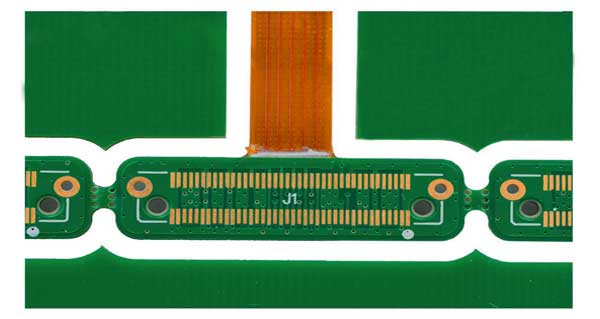
Copper is etched to form traces. For fine-line flex PCB manufacture, line width and spacing control becomes more sensitive than in many rigid boards. - Coverlay And Surface Protection
Coverlay is laminated to protect copper traces. In some designs, flexible solder mask may also be used, but coverlay remains common for durability. - Drilling, Plating, And Profiling
Holes, slots, and outline routing are completed with close attention to registration, especially for dynamic bend areas and rigid-flex transitions. - Surface Finish
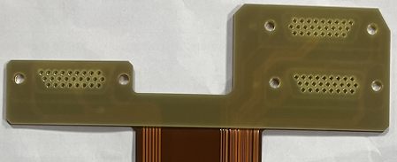
ENIG, immersion tin, OSP, and other finishes are selected based on assembly method, pad planarity, and end-use conditions. - Stiffener Lamination And Final Inspection
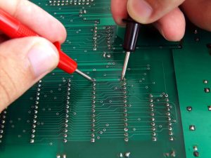
Stiffeners support connectors, components, and insertion zones. Final checks include dimensional inspection, appearance, impedance where required, and electrical test.
Key Process Focus
| Stage | Main Control Point | Why It Matters |
|---|---|---|
| Data review | Bend area rules | Prevents copper cracking |
| Material selection | PI, copper type | Affects flexibility and life |
| Coverlay | Opening accuracy | Protects pads and traces |
| Stiffener bonding | Position tolerance | Supports assembly stability |
| Final test | Continuity and fit | Reduces build risk |
In real projects, speed should not mean skipping engineering review. A reliable quick turn flex PCB manufacturer compresses the timeline by reducing iteration, not by reducing process discipline. That is what separates fast delivery from rushed delivery.


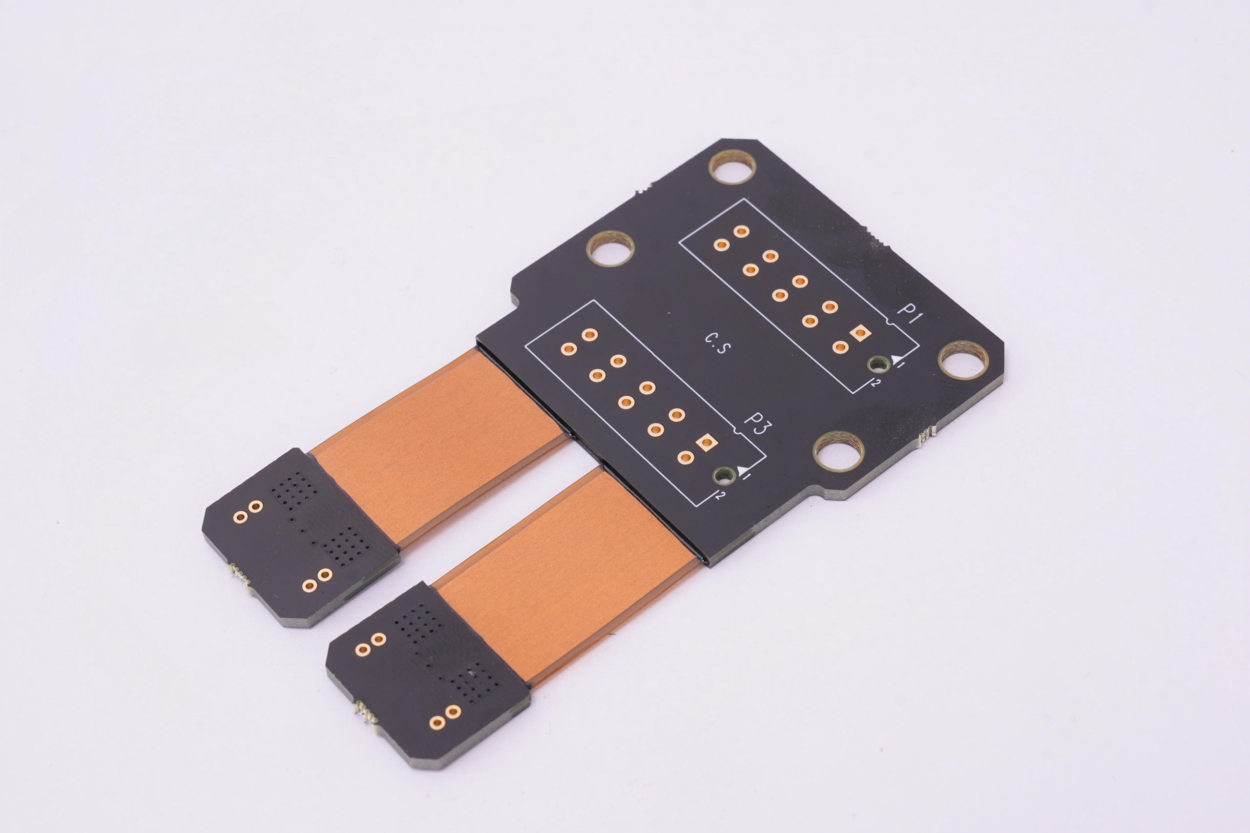
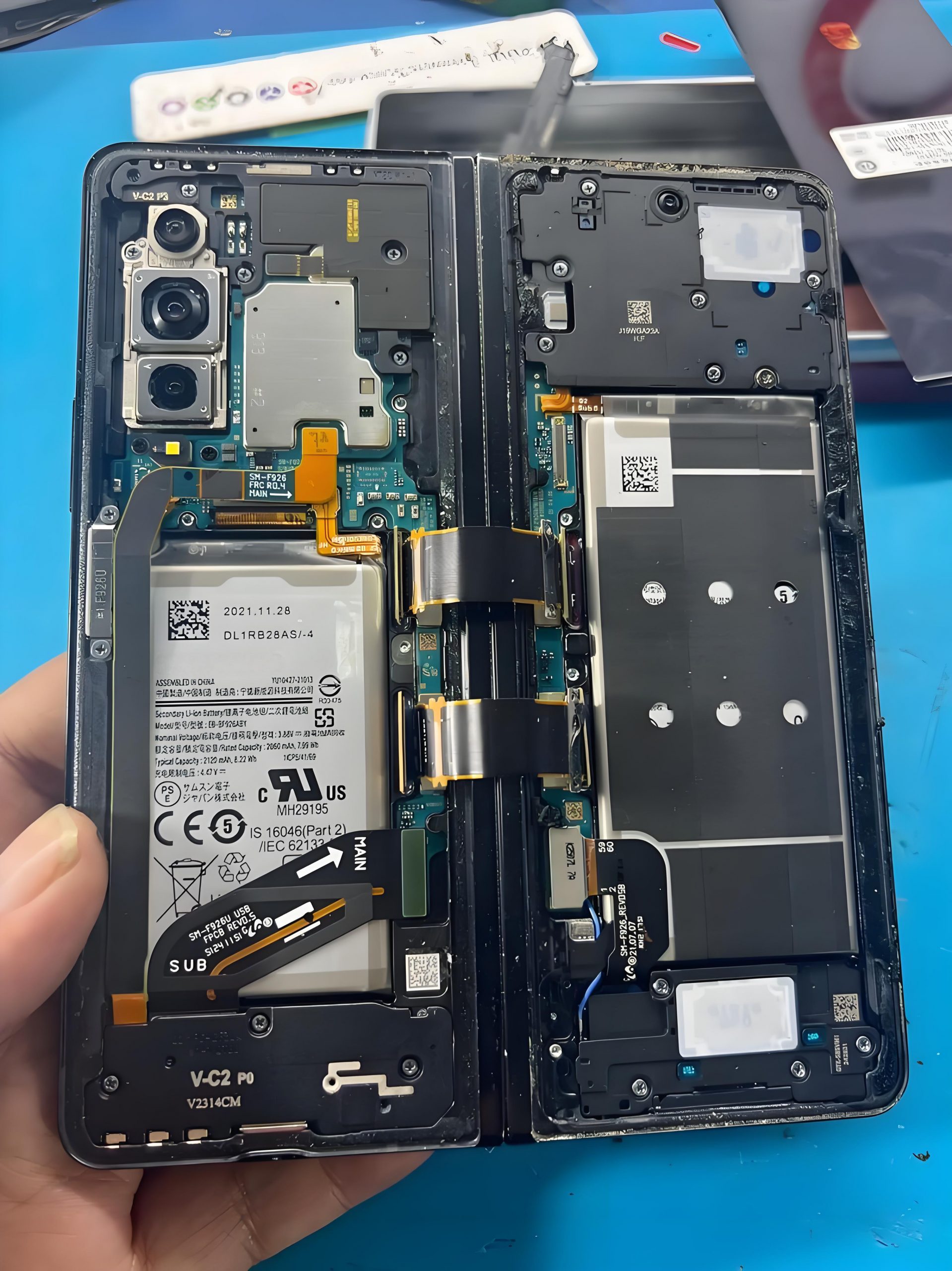
What Is The Recommended Bend Radius For A Flex PCB In Rigid-Flex Designs?
The recommended bend radius for a flex PCB in rigid-flex designs depends mainly on flex thickness, copper thickness, and whether the bend is static or dynamic. If the bend radius is too small, the copper traces and dielectric layers may experience excessive mechanical stress, which can lead to trace cracking, delamination, or early fatigue failure.
A commonly used engineering guideline is:

Where:
- R = Minimum bend radius
- T = Total thickness of the flex section
- k = Design factor depending on application
Typical values are:
| Application Type | Recommended k Value |
|---|---|
| Static bend (installed once) | 6–10 |
| Dynamic bend (repeated movement) | 10–20 |
For example, if the flex section thickness is 0.20 mm, the recommended bend radius is:
- 1.2–2.0 mm for static bending
- 2.0–4.0 mm or more for dynamic bending
Suppose the flex section thickness is 0.20 mm.
For a static bend:

to

For a dynamic bend:

to

In rigid-flex PCB manufacturing, engineers should also avoid placing vias, components, or sharp trace corners in bend areas, and consider using rolled annealed copper for better flexibility. Early design review with an experienced quick turn flex PCB manufacturer helps ensure the bend structure is both manufacturable and reliable.
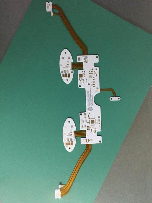
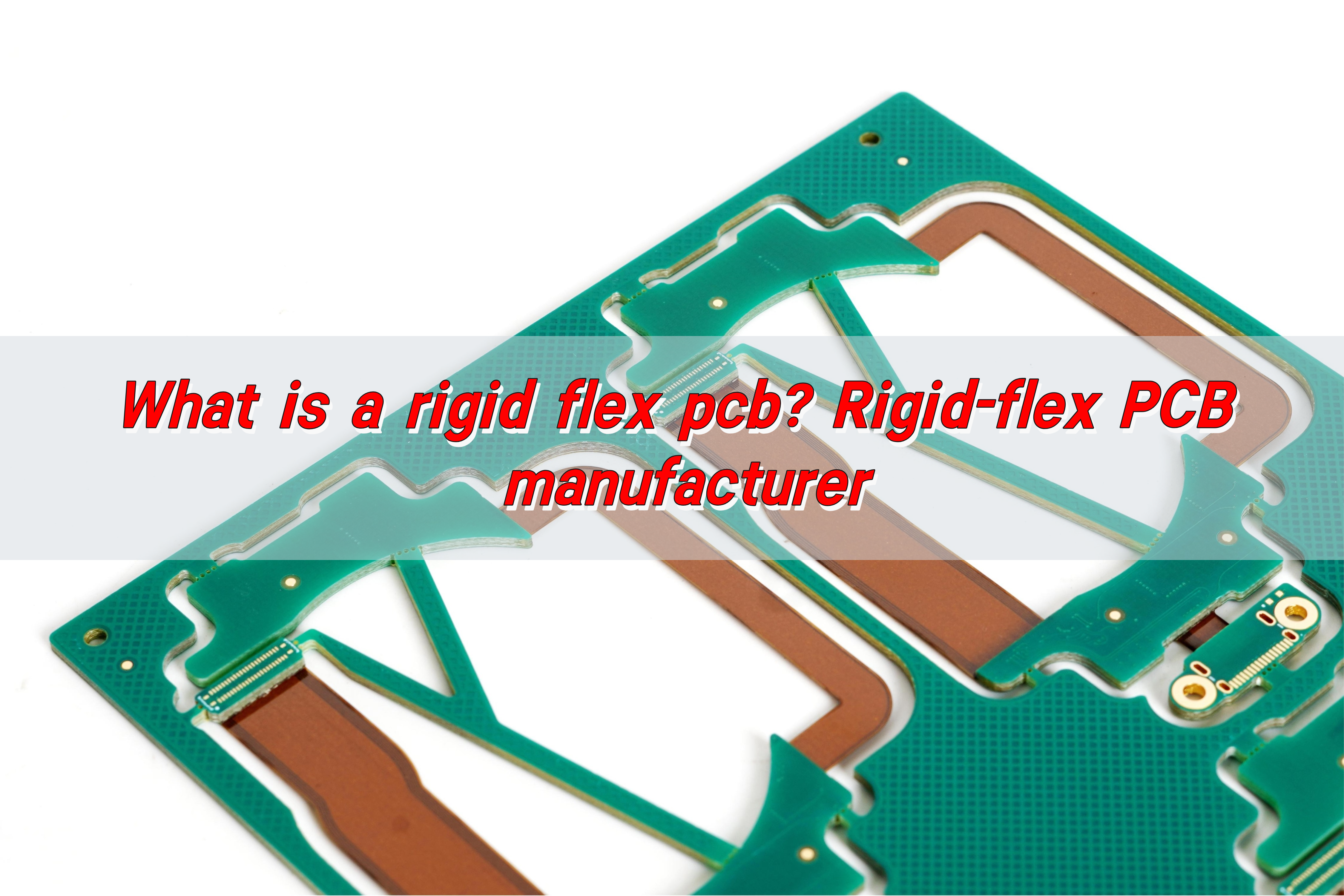
What Should Engineers Consider When Choosing A Best Rigid Flex PCB Manufacturer?
Choosing the best rigid flex PCB manufacturer is less about marketing language and more about process competence. Rigid-flex structures combine the fabrication challenges of rigid boards with the mechanical demands of flex circuits. A supplier that handles only simple boards may struggle when the design includes multilayer transitions, controlled impedance, HDI features, or repeated bending.
Engineers should focus on these evaluation points:
- Rigid-Flex Build Experience
Ask how often the supplier builds multilayer rigid-flex designs, not just simple flex tails. - Stack-Up Engineering Support
A good supplier helps optimize copper balance, adhesive system, coverlay structure, and rigid-flex transition design. - Bend Reliability Control
Trace orientation, neutral bend axis planning, and copper thickness selection all matter. - Assembly Compatibility
The manufacturer should understand how the board will be handled during SMT, fixture support, and final installation. - Inspection And Test Capability
AOI, flying probe, impedance testing, dimensional inspection, and microsection analysis improve confidence. - Prototype To Volume Path
A prototype-friendly factory should also support repeatable small-batch production.
Supplier Evaluation Snapshot
| Evaluation Item | What To Ask |
|---|---|
| Process experience | How many rigid-flex builds per month? |
| Engineering support | Do you provide stack-up and DFM feedback? |
| Quality control | Do you run microsection and reliability checks? |
| Assembly support | Can you handle one-stop PCB assembly? |
| Delivery model | Can prototype and small batch stay in one system? |
A rigid-flex PCB manufacturer should not be judged only by price or nominal lead time. The real value comes from whether the supplier can protect reliability before the board reaches assembly and field use.
How To Choose A Reliable Quick Turn Flex PCB Manufacturer For Prototype And Small Batch Projects?
A reliable quick turn flex PCB manufacturer should help you win time at the prototype stage without creating hidden problems for the next build. For prototype and small batch projects, responsiveness is important, but engineering alignment is even more important.
Here is a practical selection framework:
- Check Response Speed To Technical Questions
Fast quoting alone is not enough. The supplier should respond clearly to questions about bend radius, coverlay openings, stiffeners, and finish options. - Review DFM Depth
A valuable DFM report flags unsupported pads, sharp trace corners in bend zones, improper via placement, and risky copper distribution. - Confirm Prototype-Friendly Production Setup
Low-volume projects need flexible tooling, manageable MOQ, and engineering support rather than mass-production assumptions. - Verify One-Stop Support
When the same partner handles PCB fabrication and assembly, issues such as panel support, carrier design, and component placement near flex zones are solved earlier. - Look At Material And Process Transparency
A good supplier explains what material system is being used and why. That matters for both cost and performance.
What Reliable Quick Turn Support Looks Like
- Fast engineering review
- Clear manufacturability feedback
- Stable prototype lead time
- Flexible small-batch support
- Joined-up PCB plus assembly workflow
For many development teams, a quick turn flex PCB manufacturer is valuable not because the board arrives fast, but because the prototype arrives usable, buildable, and ready for the next step.
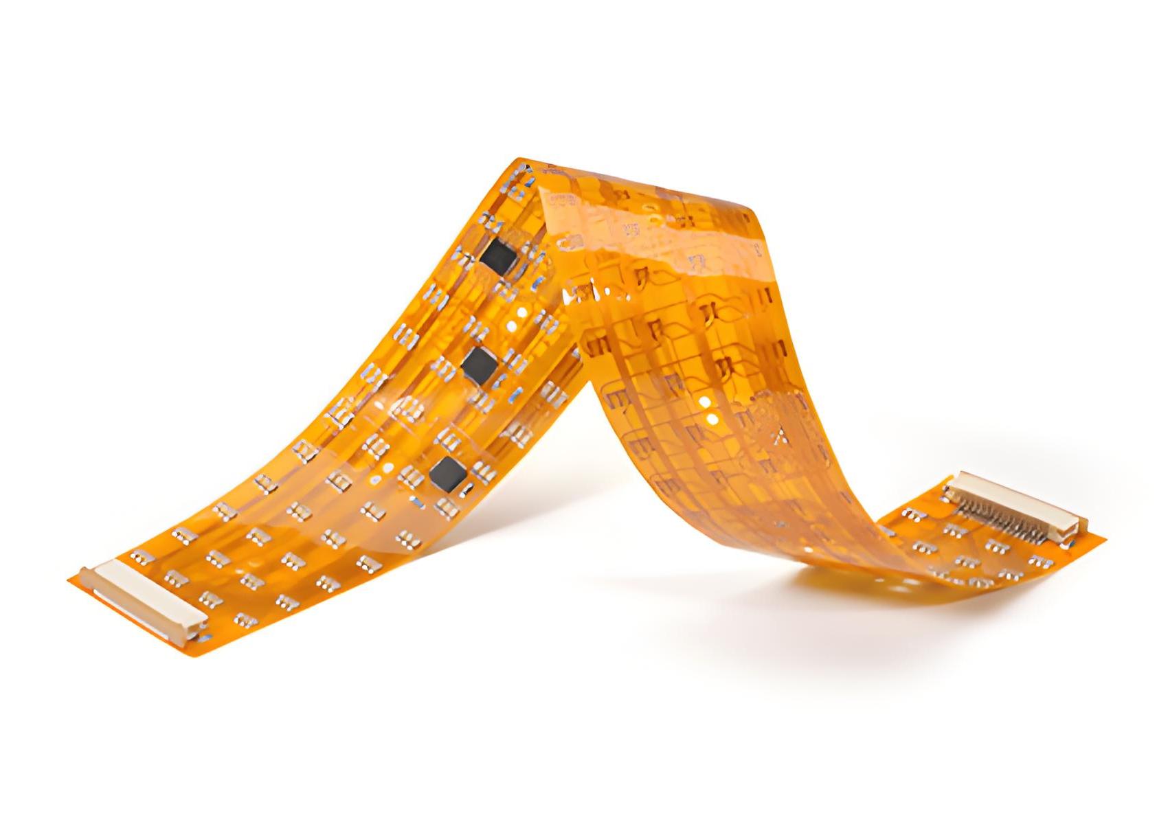
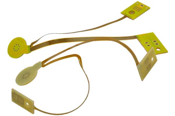
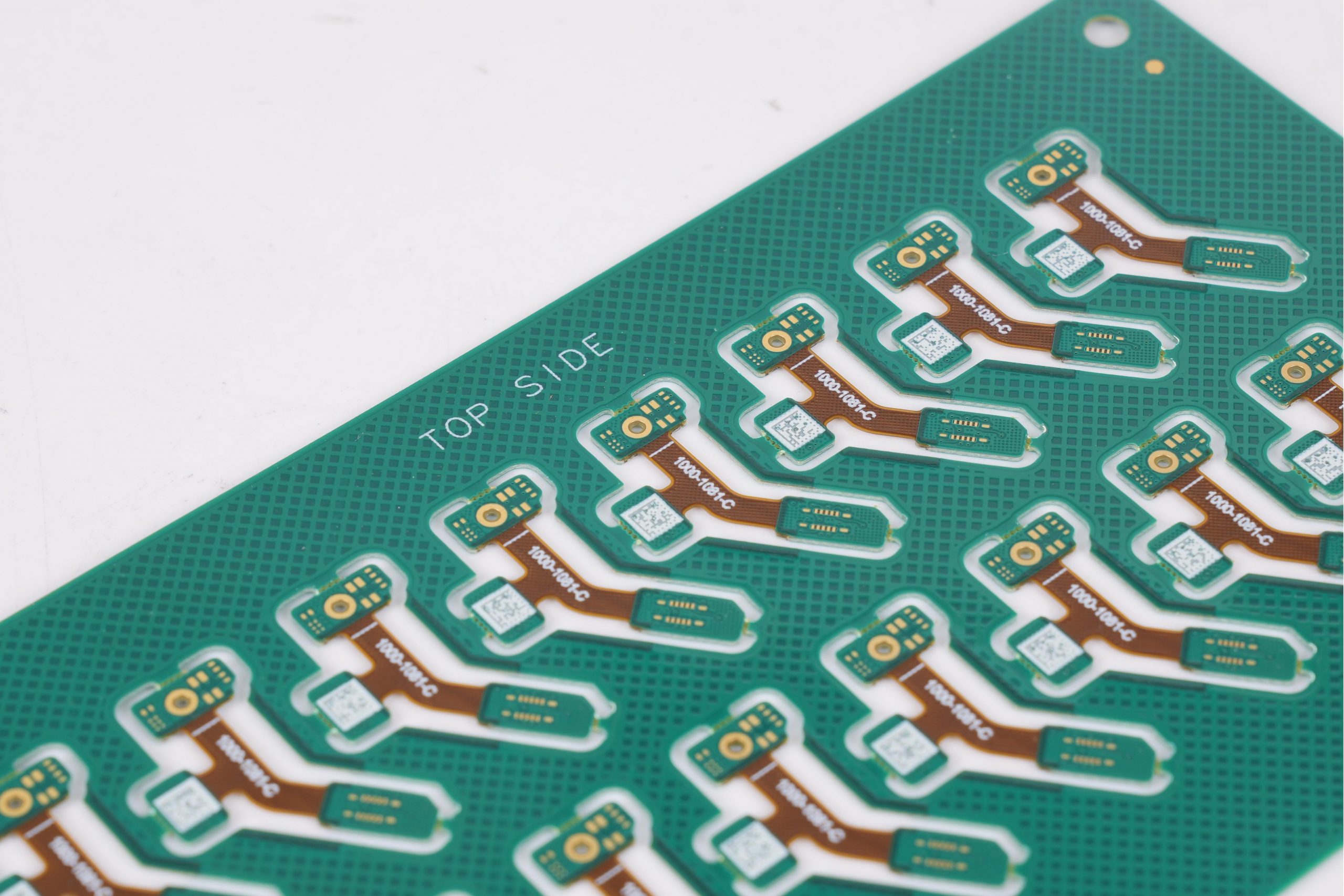
What Technical Capabilities Should A Professional Flex PCB Manufacturer Provide?
A professional flex PCB manufacturer should offer more than basic etching and lamination. Technical capability is what determines whether the supplier can handle real engineering demands across product categories such as medical devices, industrial controls, wearables, telecom modules, and semiconductor equipment.
Core capabilities typically include:
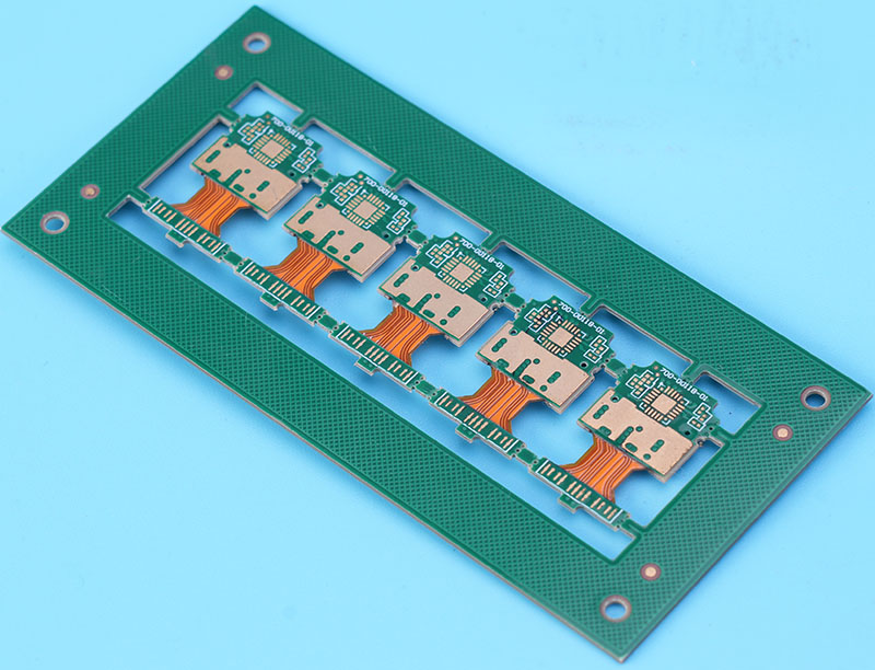
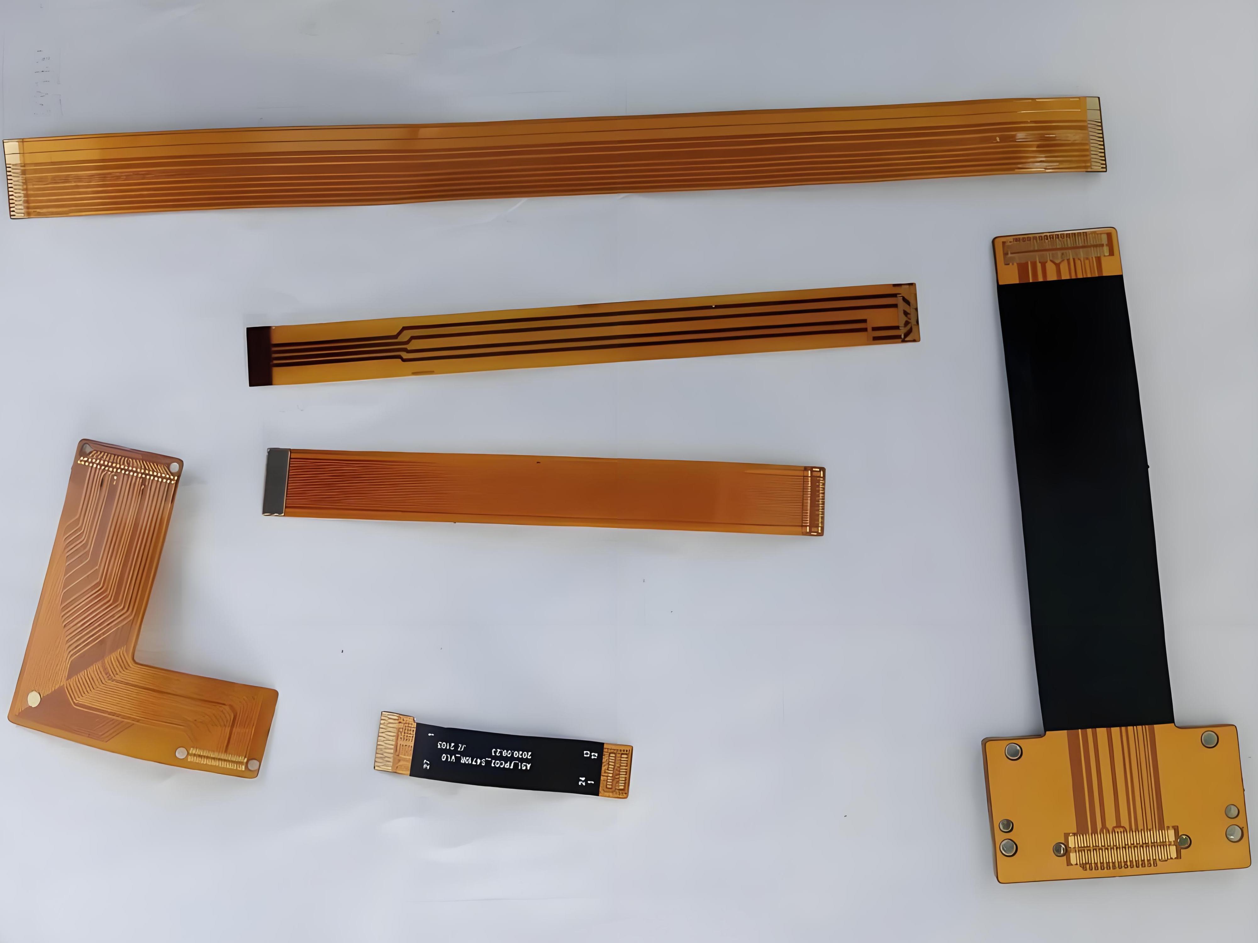
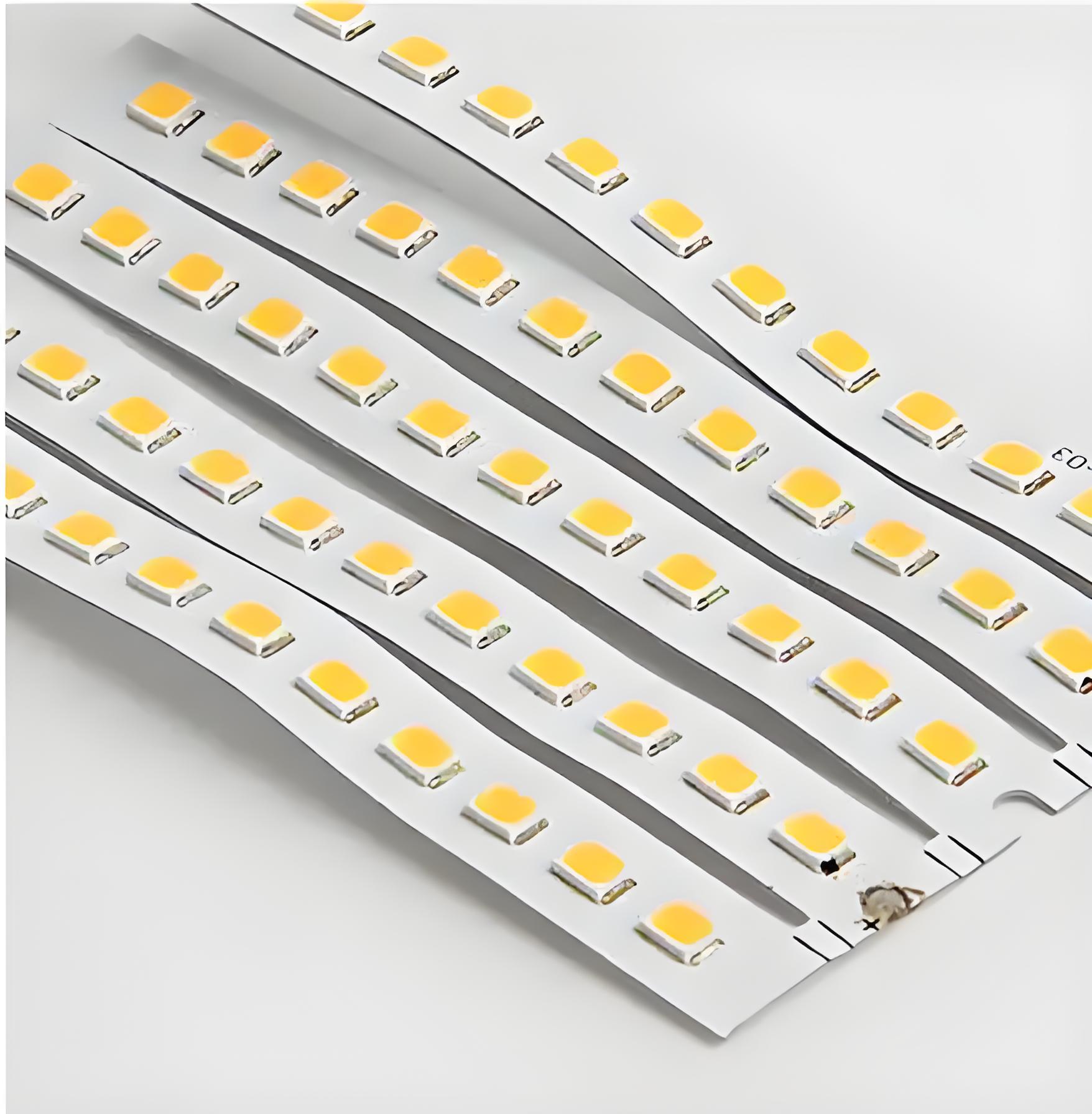
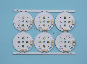
- Single-sided, double-sided, and multilayer flex PCB manufacturing
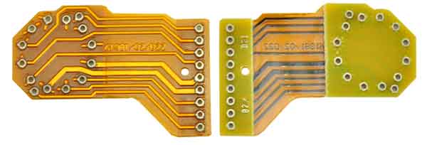
- Rigid-flex and flex-rigid PCB structures
- Fine-line trace capability for compact layouts
- Coverlay processing and selective stiffener support
- Controlled impedance for high-speed or RF interconnects
- SMT-ready pad finish and assembly-friendly design support
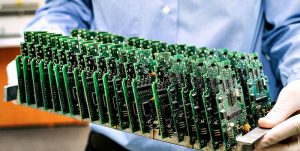
- Prototype through low-volume production service
Capability Reference Table
| Capability | Typical Value Focus |
|---|---|
| Base material | Polyimide systems |
| Copper type | Rolled annealed preferred for bend zones |
| Layer count | Single to multilayer |
| Structure type | Flex, rigid-flex, flex-rigid |
| Build support | DFM, stack-up, assembly review |
In advanced projects, flex PCB manufacturing capabilities also include dimensional control, IPC-oriented workmanship, fixture planning, and process traceability. This matters even more when evaluating a semiconductor flex PCB manufacturer or a supplier supporting compact computing systems.
A supplier with real technical range will also understand when not to overbuild. Sometimes the best solution is not the most complex one. It is the one that meets bend life, assembly stability, and cost targets at the same time.
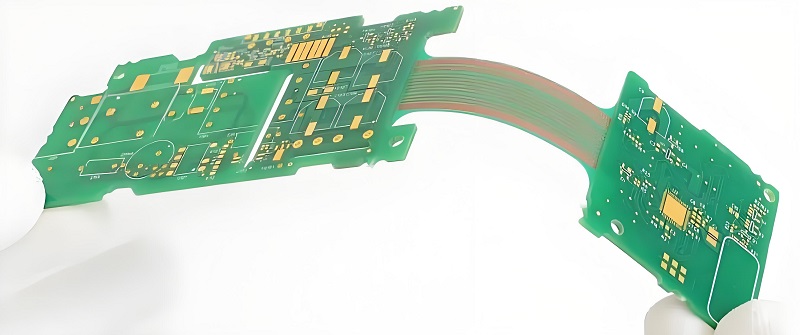
What Are The Key Differences Between A Rigid Flex PCB Manufacturer And A Standard PCB Supplier?
A standard PCB supplier may produce excellent rigid boards, but that does not automatically qualify them as a rigid-flex PCB manufacturer. The materials, process controls, and failure modes are different.
The key differences usually appear in these areas:
1. Material System Knowledge
Rigid-flex boards involve polyimide flex cores, adhesive systems, coverlay, stiffeners, and transition-zone design. Standard suppliers may be less experienced in these combinations.
2. Mechanical Reliability Thinking
Rigid-flex design is not purely electrical. Bend stress, copper fatigue, and unsupported trace geometry must be considered early.
3. Registration And Lamination Complexity
Registration across rigid and flex sections is more demanding. Lamination windows are tighter.
4. Assembly Planning
A rigid-flex PCB manufacturer should anticipate carriers, support fixtures, and component keep-out rules for flex areas.
5. Inspection Depth
Microsection review and transition-zone inspection are more important in rigid-flex builds than in ordinary rigid boards.
Quick Comparison
| Item | Standard PCB Supplier | Rigid Flex PCB Manufacturer |
|---|---|---|
| Main focus | Rigid boards | Rigid + flex integration |
| Material expertise | Conventional laminates | PI, coverlay, stiffeners |
| Mechanical design awareness | Limited | High |
| Bend-zone control | Rare | Essential |
| Assembly planning | Basic | Structure-aware |
This difference is why engineers should be careful when comparing quotes. A lower price from a standard supplier may not reflect the real technical risk.
What Are The Critical Steps In The Rigid Flex PCB Manufacturing Process That Affect Reliability?
The rigid flex PCB manufacturing process affects long-term reliability most strongly at a few specific control points. If these steps are stable, the board has a much better chance of surviving both assembly and end-use stress.
The most critical steps include:
- Stack-Up Definition
Layer build, copper thickness, adhesive structure, and rigid-to-flex transition must be engineered together. - Lamination Control
Pressure, temperature, and material flow affect dimensional stability and bonding quality. - Drill And Plated Hole Integrity
Hole wall quality and plating reliability are essential, especially near rigid-flex interface regions. - Coverlay And Flex Area Registration
Misregistration can expose copper or weaken pad protection. - Outline Routing And Transition Shaping
Poorly designed corners or stress concentration points reduce bend life. - Surface Finish Compatibility
Finish choice must match both assembly method and functional environment. - Final Structural Inspection
Electrical test alone is not enough. Mechanical and dimensional verification also matter.
Reliability Risk Map
| Process Step | Common Risk | Reliability Impact |
|---|---|---|
| Stack-up design | Wrong copper balance | Warpage or stress |
| Lamination | Poor bonding | Delamination |
| Drilling/plating | Hole weakness | Interconnect failure |
| Coverlay | Offset opening | Pad exposure risk |
| Routing | Stress points | Crack initiation |
For rigid flex PCB manufacturing, reliability is rarely decided by one dramatic error. It is usually shaped by whether small process details were handled correctly, one after another.
What Design Rules Should Engineers Follow When Working With A Flex Rigid PCB Manufacturer?
When working with a flex rigid PCB manufacturer, good design rules reduce both fabrication difficulty and field failure risk. Many layout issues are avoidable if they are addressed before production release.
Important design rules include:
- Use Smooth Trace Routing In Bend Areas
Avoid sharp corners. Curved routing distributes stress better. - Keep Vias Out Of Dynamic Bend Zones
Vias create local stress concentration and reduce flexibility. - Control Copper Thickness Carefully
Thicker copper may improve current handling but reduces bend performance. - Plan Bend Radius Rationally
A common engineering rule is that minimum bend radius increases with thickness and whether bending is static or dynamic. - Stagger Traces Where Possible
This can reduce I-beam effect and improve flex behavior. - Protect Transition Areas
Rigid-to-flex interfaces need good support and geometry control. - Reserve Space For Stiffeners And Assembly Support
Connector zones often need reinforcement.
Simple Rule Guide
| Design Item | Preferred Practice |
|---|---|
| Trace corner | Use arcs, not sharp angles |
| Via location | Keep out of bend zone |
| Copper in bend area | Use balanced layout |
| Bend radius | Match thickness and use case |
| Stiffener zones | Plan early in layout |
For practical engineering, the best design rule is early collaboration. A flex rigid PCB manufacturer can often spot a risk in minutes that would otherwise cost days in rework.
Why Do Many Global OEMs Choose A Flex PCB Manufacturer China For Rapid PCB Production?
Many global OEMs choose a flex PCB manufacturer China partner because China remains highly competitive in response speed, material ecosystem access, engineering support density, and one-stop production capability. The decision is not only about labor cost. It is often about supply chain efficiency.
Key reasons include:
- Fast Prototype Turnaround
Shorter internal coordination paths can accelerate quoting, tooling, fabrication, and assembly. - Dense Material And Component Supply Chain
This supports rapid sourcing for prototype PCB assembly and small-batch builds. - Broad Process Coverage
Many suppliers can support flex PCB manufacture, rigid-flex PCB manufacturing, SMT, testing, and box-level integration. - Engineering And Manufacturing Proximity
DFM feedback, process adjustments, and material substitutions can move faster. - Scalable Cost Structure
Prototype, pilot run, and repeat orders can often stay within one supplier network.
Why China Remains Strong
| Factor | Practical Benefit |
|---|---|
| Supply chain density | Faster sourcing |
| Process integration | Fewer handoff delays |
| Prototype capacity | Better quick turn support |
| Technical manpower | Faster DFM response |
| Scale flexibility | Good for small batch and growth |
That said, supplier selection still matters. Not every flex PCB manufacturer China option offers the same engineering quality. The right partner should combine speed, communication, process discipline, and one-stop PCB assembly support.
All in all, quick turn flex PCB manufacturer capability is important because it helps engineering teams shorten development cycles while protecting flex and rigid-flex board reliability through better process control and joined-up manufacturing support. This article covered the flex PCB manufacturing process, supplier evaluation logic, rigid-flex reliability controls, design rules, and the practical reasons many OEMs choose integrated one-stop production partners.
EBest Circuit (Best Technology) supports customers with flex PCB manufacturing, rigid flex PCB manufacturing, DFM review, component sourcing, and one-stop PCB assembly for prototype and small-batch projects. If you need a responsive manufacturing partner with practical engineering support and reliable execution, pls feel free to contact us via sales@bestpcbs.com.
FAQs About Quick Turn Flex PCB Manufacturer
How Fast Can A Quick Turn Flex PCB Manufacturer Deliver Prototypes?
Prototype lead time typically ranges from 3–7 working days, depending on layer count, board complexity, and material availability. Simple single-layer flex PCBs can sometimes be completed in as little as 48–72 hours, while multilayer rigid-flex boards may require slightly longer due to lamination and inspection steps.
Can A Quick Turn Flex PCB Manufacturer Also Provide PCB Assembly Services?
Yes. Many advanced suppliers provide one-stop PCB assembly, including PCB fabrication, component sourcing, SMT assembly, testing, and inspection. Working with a single flex PCB assembly manufacturer helps reduce coordination delays and improves reliability during prototype and small-batch production.