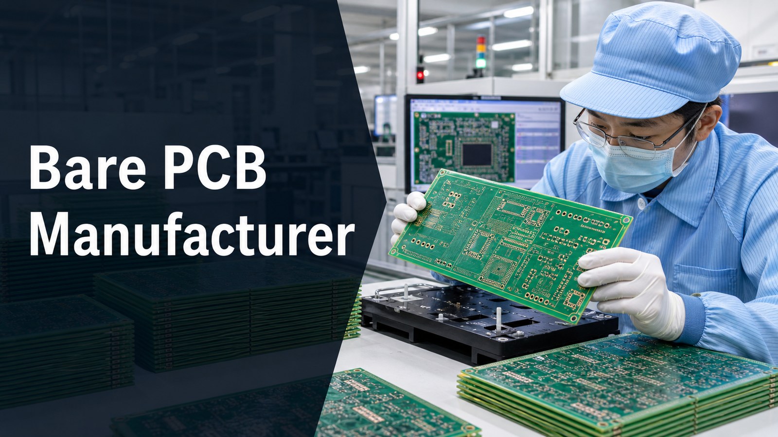
A bare PCB manufacturer fabricates unpopulated printed circuit boards and verifies the board before components are mounted. For buyers, the important decision is not only who can make the board, but who can check the Gerber files, material, copper, holes, surface finish, solder mask, test plan and quote assumptions before production starts.
EBest Circuit supports bare PCB projects from file review through fabrication, electrical test and later PCBA support when the same design needs assembly after the board is approved. This article explains what to check before choosing a bare PCB manufacturer and what to send for a practical RFQ.
What can go wrong when a bare PCB order is treated as a simple board purchase?
Many bare board problems appear before assembly, but buyers often discover them only when components are already waiting.
- Gerber, drill, stackup and drawing files do not describe the same revision, causing quote assumptions to drift.
- Material, Tg, board thickness, copper weight or surface finish is selected without checking manufacturability.
- Fine line, spacing, hole size, solder mask bridge or outline tolerance is pushed too close to the process limit.
- The buyer orders bare boards first, then discovers assembly, stencil, fixture or test needs were not considered.
- Electrical test, impedance, panelization or packaging requirements are not stated clearly enough for production.
EBest Circuit helps buyers turn bare PCB files into a controlled manufacturing package.
- We review Gerber or ODB++ files, drill data, stackup, copper, board thickness, surface finish and solder mask requirements before quote assumptions are locked.
- We can discuss FR4 low Tg, mid Tg and high Tg material routes, including when a high Tg or higher-layer design needs extra review.
- We check common manufacturability items such as 4/4mil line and spacing, finished hole size, through-hole aspect ratio, solder mask bridge, panelization and test needs.
- We connect bare PCB fabrication with assembly planning when the buyer also needs BOM, CPL, stencil, component sourcing, inspection or functional test support.
- We keep quote questions visible early, so buyers can compare suppliers by risk, not only by unit board price.
What a Bare PCB Manufacturer Should Deliver
A bare PCB manufacturer should deliver manufacturable boards that match the released files and are ready for assembly, testing or product validation.
A useful supplier does more than image copper and ship boards. It should review file completeness, stackup, laminate, copper weight, drill data, solder mask, silkscreen, surface finish, outline, panelization and electrical test requirements. For FR4 projects, buyers can also compare whether the supplier can support the material and process route shown in the design, such as standard FR4 PCB, high Tg FR4, heavier copper or tighter spacing.
Is a Bare PCB the Right Order Type for Your Project?
A bare PCB order is right when you need fabricated boards without mounted components, or when you want to approve the board before assembly starts.
| Project Situation | Order Fit | Buyer Check |
|---|---|---|
| Design validation before component build | Bare PCB can fit well | Confirm test coupons, dimensions and finish |
| Buyer has an assembly partner already | Bare PCB is often enough | Share assembly constraints before fabrication |
| Prototype then PCBA later | Bare PCB first, PCBA later | Keep BOM, CPL and stencil needs visible early |
| Turnkey electronic product build | PCBA or turnkey route may fit better | Quote board and assembly together |
Bare PCB vs PCB Assembly: What Buyers Should Separate
Bare PCB manufacturing makes the unpopulated board; PCB assembly mounts and solders components onto that board.
Separating these scopes helps avoid unclear quotes. Bare PCB questions include material, layer count, copper, holes, surface finish and electrical test. Assembly questions include BOM, CPL, stencil, polarity, package size, soldering method, inspection and functional test. If the same project will later move into assembly, connect the bare board review with the PCB manufacturing and assembly plan early.
Bare PCB Manufacturing Capabilities at a Glance
Capability should be checked against the exact design, but a useful RFQ can start from material, layer count, copper, thickness, holes, line width and surface finish.
| Capability Area | Verified Example | RFQ Note |
|---|---|---|
| Material | FR4 low Tg, mid Tg and high Tg routes listed | Confirm laminate and Tg with the design environment |
| Layer count | FR4 high Tg common range includes 1-10 layers | Higher layer counts require project review |
| Copper | Inner HOZ-5OZ and outer 1OZ-5OZ listed as common ranges | Heavier copper affects spacing, etching and cost |
| Finished hole | 0.2mm common example; 0.15mm special review route | Check annular ring, aspect ratio and tolerance |
| Line width / spacing | 4/4mil common examples; 3/3mil special route | Do not quote tight designs without DFM review |
| Surface treatment | OSP, HASL, ENIG, immersion silver, immersion tin, ENEPIG and hard gold options listed | Choose around assembly, storage and reliability needs |
What Can Go Wrong Before Components Are Mounted
Bare board defects can block assembly even when no components have been placed yet.
Common risks include wrong revision files, missing drill data, copper spacing that cannot support the requested copper weight, solder mask openings that affect pads, unclear impedance or electrical test requirements, board outline issues, and surface finish choices that do not match storage or soldering needs. The earlier these are reviewed, the easier it is to fix them before production cost is committed.
How EBest Circuit Helps Buyers Control Bare PCB Risk
EBest Circuit helps by checking manufacturing details before the buyer treats the quote as final.
Send the Gerber or ODB++ files, drill files, stackup, drawing, board thickness, copper, surface finish, quantity and inspection needs. If the board will later become an assembled product, send BOM and CPL as well so fabrication decisions do not create avoidable assembly problems.
Materials, Layer Count and Board Thickness
Material and thickness decisions should match electrical, mechanical, thermal and assembly requirements.
FR4 is common for many bare PCB projects, but Tg grade, laminate family, prepreg, layer count and finished thickness still matter. The verified capability source lists FR4 low Tg, mid Tg and high Tg material routes, with higher-layer or special material designs requiring review. Finished thickness also depends on the process and surface finish route, so buyers should not send only a board outline and expect a complete quote.
Copper Weight, Line Width, Spacing and Hole Design
Copper and drill choices should be checked together because one change can affect spacing, plating, cost and reliability.
For common FR4 routes, the capability source lists inner copper examples from HOZ to 5OZ and outer copper examples from 1OZ to 5OZ, with heavier copper requiring review. It also lists 4/4mil line width and spacing as common examples and 3/3mil as a special review route. Buyers should send copper weight, current requirements, minimum trace/space, finished hole size and tolerance expectations together.
Surface Finish, Solder Mask and Silkscreen Choices
Surface finish, solder mask and silkscreen choices affect solderability, inspection, storage and assembly readiness.
Common surface treatment options include OSP, HASL, ENIG, immersion silver, immersion tin, ENEPIG and hard gold fingers. Solder mask color can also matter when optical inspection, LED reflection, branding or contrast is important. The RFQ should state the preferred finish, mask color, legend requirements and any storage or assembly constraints.
Bare PCB Fabrication Process
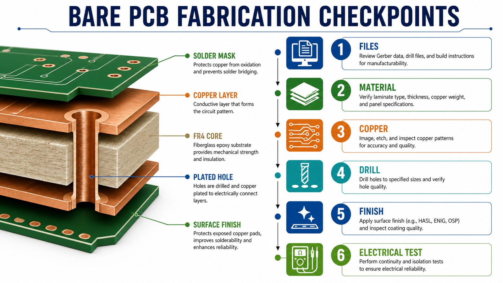
The bare PCB fabrication process should move from file review to material preparation, imaging, etching, drilling, plating, solder mask, surface finish and final inspection.
The useful question for buyers is not only the order of steps. It is where each step can change the result. Material choice affects stackup. Copper affects etching and spacing. Drilling affects plating and reliability. Surface finish affects solderability. Electrical test confirms open and short risk before the bare boards move to assembly.
Testing and Inspection Before Shipment
Bare PCB testing should confirm that the unpopulated board is electrically and visually ready for the next build stage.
Depending on the design, inspection may include visual checks, AOI, dimensional checks, solder mask checks, electrical test, impedance review or sample-level confirmation. Buyers should specify whether every board needs electrical test, whether test reports are required and whether packaging must protect the board finish for later assembly.
Cost Factors for Bare PCB Manufacturing
Bare PCB cost changes with material, layer count, copper, board size, hole density, surface finish, tolerance, test and quantity.
| Cost Factor | Why It Matters | What to Send |
|---|---|---|
| Material and Tg | Changes laminate cost and process route | Laminate preference or operating requirement |
| Layer count | Changes lamination and drilling complexity | Stackup and impedance needs |
| Copper weight | Affects etching, spacing and plating | Inner and outer copper requirements |
| Surface finish | Affects solderability and shelf life | OSP, HASL, ENIG or other finish preference |
| Testing | Adds inspection work and reduces shipment risk | Electrical test, impedance or report needs |
Prototype, Low-Volume and Production Order Planning
Prototype and production bare PCB orders should be planned differently because the risk is not always the same.
Prototype orders often need fast DFM feedback, revision control and clear questions before the design is released. Production orders need stable specifications, panelization, repeatable test requirements, packaging and supplier communication. If the design will later require mounted parts, use early board feedback to prepare the later prototype PCB assembly or production assembly route.
How to Evaluate a Bare PCB Manufacturer
A bare PCB manufacturer should be evaluated by DFM response, capability fit, file discipline, testing clarity and communication quality.
- Does the supplier ask clear questions before quoting unclear files?
- Can it support the material, copper, line width, spacing, hole and thickness requirements?
- Does it explain when a requirement needs special review instead of silently accepting it?
- Can it connect bare board fabrication with later assembly planning when needed?
- Does the quote state surface finish, testing, quantity, revision and delivery assumptions clearly?
RFQ Checklist for Bare PCB Manufacturing
A useful bare PCB RFQ should include the files and constraints that affect manufacturability, price and shipment risk.
- Gerber or ODB++ files, drill files and fabrication drawing
- Stackup, layer count, material, Tg requirement and board thickness
- Copper weight, minimum line width/spacing, finished hole size and tolerance needs
- Surface finish, solder mask color, silkscreen and special process requirements
- Quantity, revision, panelization preference, electrical test and inspection report needs
- BOM, CPL and assembly drawing if later PCBA support is required
FAQ About Bare PCB Manufacturers
What is a bare PCB manufacturer?
A bare PCB manufacturer fabricates unpopulated printed circuit boards before components are mounted. The work usually includes material preparation, copper patterning, drilling, plating, solder mask, surface finish, routing and electrical test.
Is a bare PCB the same as a PCB assembly?
No. A bare PCB is the circuit board without components. PCB assembly, or PCBA, mounts and solders components onto that board. Some buyers order bare boards only, while others need board fabrication plus assembly.
What files are needed for a bare PCB quote?
Send Gerber or ODB++ files, drill files, fabrication drawing, stackup, material, copper weight, board thickness, surface finish, quantity and test requirements. Add BOM and CPL if assembly planning is also needed.
Can EBest Circuit support bare PCB and later assembly?
Yes. EBest Circuit can review bare PCB manufacturability and also connect the build with component sourcing, assembly, inspection and test planning when the project needs PCBA support after board fabrication.
Need a bare PCB manufacturer for prototypes, low-volume builds or production orders? Send your Gerber or ODB++ files, drill files, stackup, material, copper, surface finish, quantity, test requirements and any later BOM/CPL needs to sales@bestpcbs.com. EBest Circuit can review DFM, fabrication risk, quote assumptions and assembly planning before production starts.
You may also like




Tags: bare pcb, pcb fabrication, PCB Quote