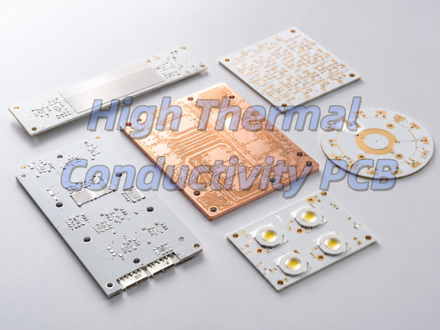
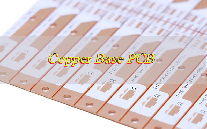
A copper base PCB helps medical diagnostic devices control heat where standard FR-4 or aluminum PCB materials cannot provide enough thermal margin. It transfers heat from power components, optical modules, heater circuits and precision control areas into a copper base for faster heat spreading.
In diagnostic equipment, heat can affect test accuracy, signal stability, optical output, solder joint life and long-term reliability. Therefore, thermal design should not be treated as an afterthought. It should be reviewed together with the stack-up, dielectric layer, copper thickness, surface finish, assembly process and reliability test plan before production starts.
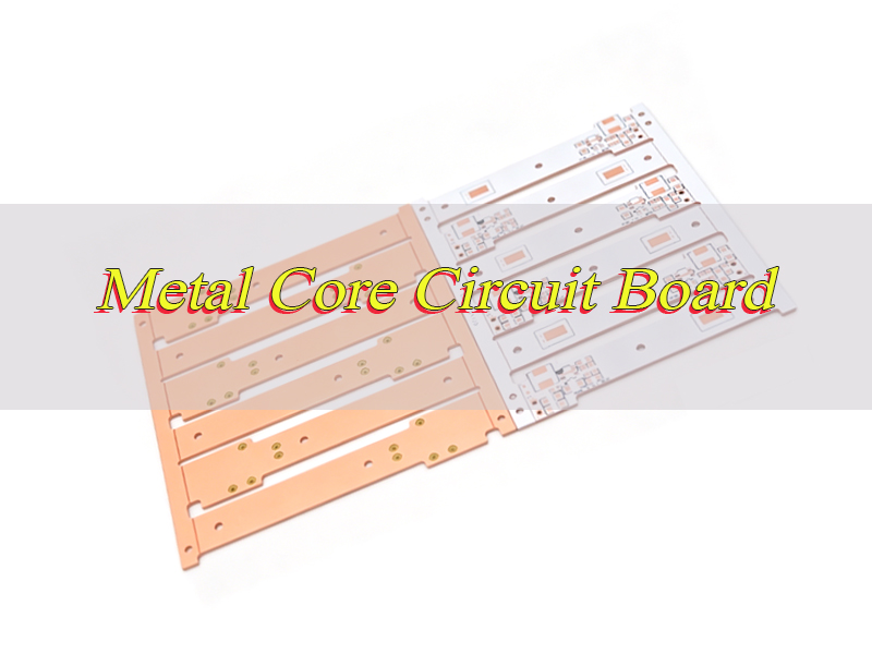
What Is a Copper Base PCB in Medical Diagnostic Devices?
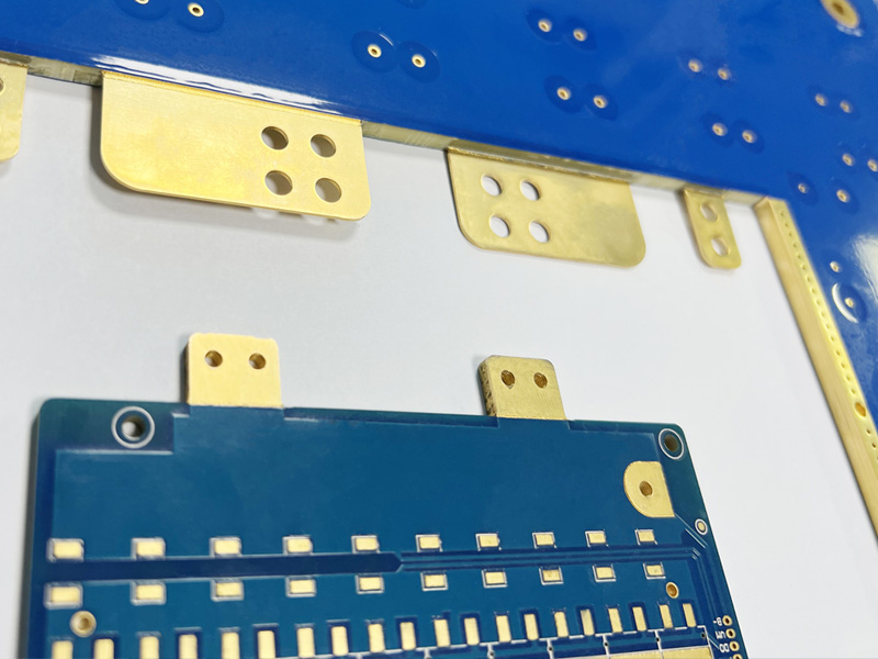
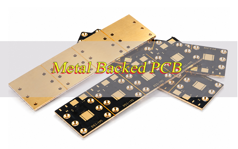
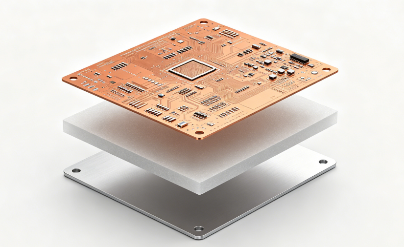
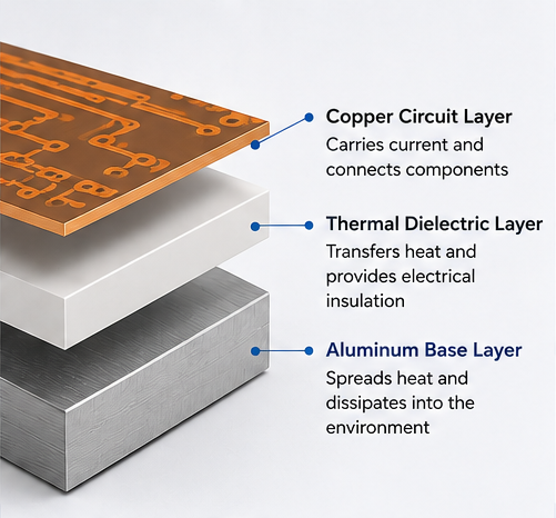
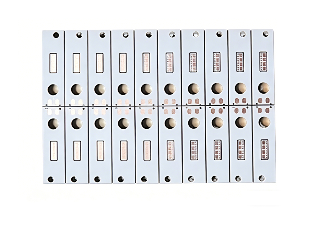
A copper base PCB is a metal substrate PCB that uses copper as the main supporting and heat-spreading base. A typical structure includes a copper circuit layer, a thermally conductive dielectric layer and a copper base layer. The circuit layer carries electrical signals, while the copper base helps move heat away from high-power components.
In medical diagnostic devices, this structure is used when compact modules need both stable electrical function and strong heat dissipation. It is suitable for optical detection, thermal control, power conversion and high-current medical electronics where temperature drift may reduce device accuracy or service life.
Why Do Medical Diagnostic Devices Need Copper Base PCB?
Medical diagnostic devices need a copper base PCB when heat directly affects accuracy, reliability or operating stability. Many diagnostic systems combine sensors, LEDs, laser diodes, heaters, motors, power modules and analog circuits in a small enclosure. Without a stable thermal path, heat can spread into sensitive areas and disturb test results.
Key reasons include:
- Improve temperature stability for optical, sensor and reagent control modules.
- Reduce hot spots around LEDs, MOSFETs, drivers and heater circuits.
- Extend component life by lowering repeated thermal stress.
- Improve solder joint reliability during continuous operation and thermal cycling.
- Support compact design where large heatsinks or fans are limited.
This makes copper substrate design valuable for high-reliability diagnostic equipment.
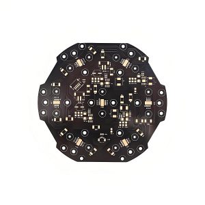
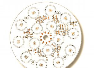
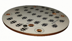
Which Medical Diagnostic Device Modules Use Copper Base PCB?
A copper base PCB is usually selected for modules that generate heat and need stable control at the same time. It is not required for every medical PCB, but it becomes important when temperature change may affect optical output, signal reading or power reliability.
Common application modules include:
- PCR and qPCR thermal control modules
- IVD analyzer heater boards
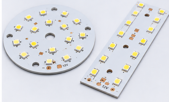
- Fluorescence detection LED boards
- Laser diode driver modules
- TEC and Peltier control boards
- Motor driver boards for pumps and scanners
- Power supply and DC-DC converter boards
- Imaging support power modules with localized high-power areas
- Blood analyzer and biochemical analyzer heating or power control modules
These modules benefit from faster heat transfer and better temperature uniformity.
What Thermal Problems Can Copper Base PCB Solve in Diagnostic Equipment?
A copper base PCB can solve thermal problems caused by localized heat, poor heat spreading and unstable component temperature. In diagnostic equipment, these problems are not only electrical risks. They may also affect optical reading, reaction control and repeat test consistency.
Main problems include:
- LED brightness drift caused by rising junction temperature.
- Sensor signal offset caused by nearby power heat.
- Reagent temperature instability in thermal control modules.
- MOSFET overheating in motor, heater or TEC driver circuits.
- PCB discoloration or solder fatigue after repeated operation.
- Enclosure hot spots caused by poor heat transfer to the chassis.
The main value is stable heat movement from the component to the copper base and then to the final cooling path.
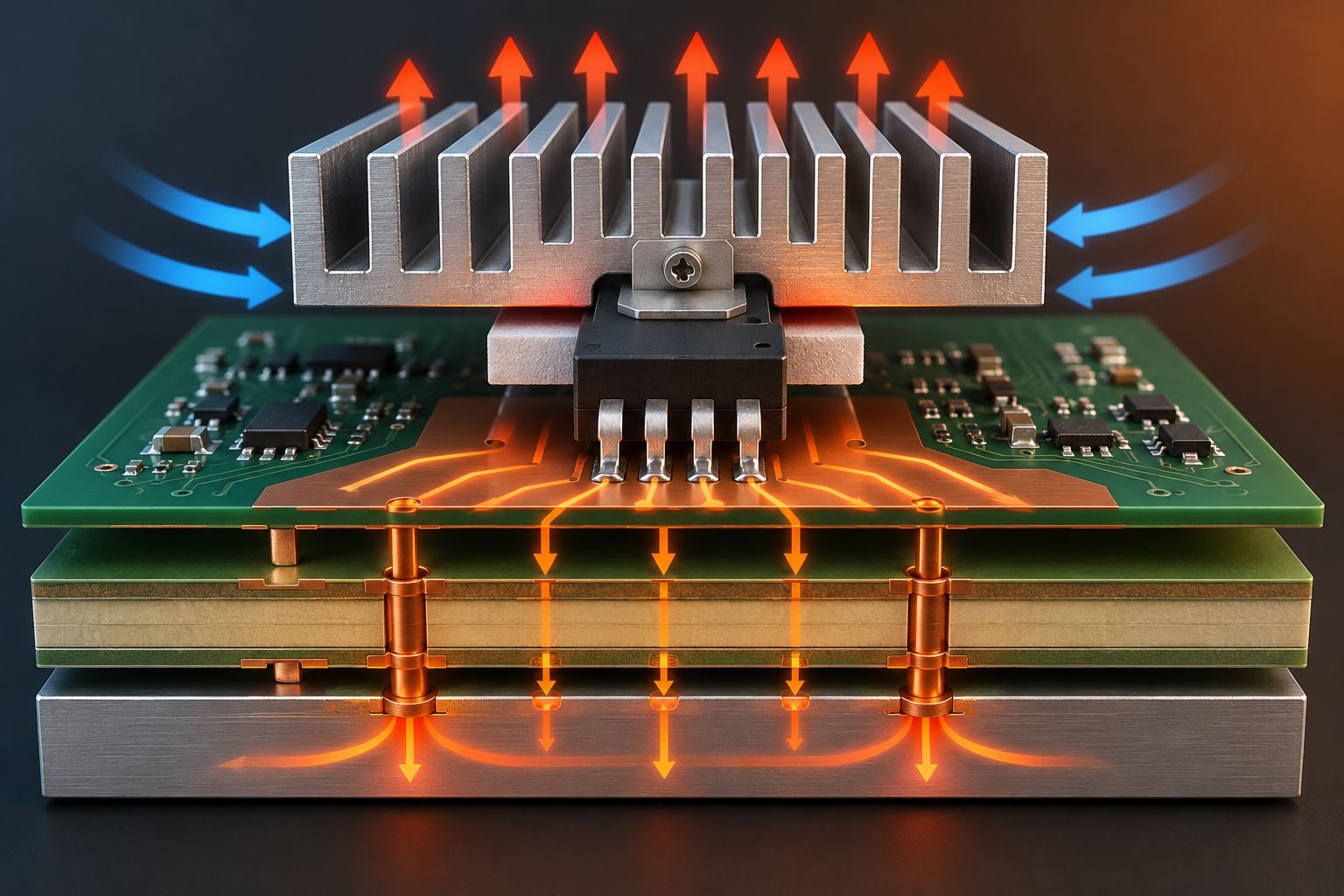
How Does Copper Base PCB Improve Heat Dissipation and Temperature Stability?
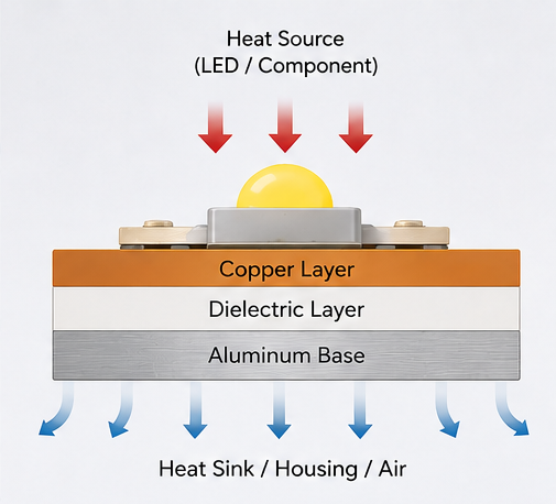
A copper base PCB improves heat dissipation by shortening the thermal path from the component to the heat-spreading base. Heat moves from the component pad to the copper circuit, passes through the thermally conductive dielectric layer and spreads across the copper base. This reduces local temperature concentration.
Copper has much better thermal conductivity than aluminum and FR-4, so it spreads heat faster across the board area. As a result, high-power components can operate at a lower and more stable temperature. For diagnostic equipment, this supports more stable optical output, lower power device stress and better long-term repeatability.
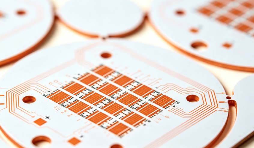
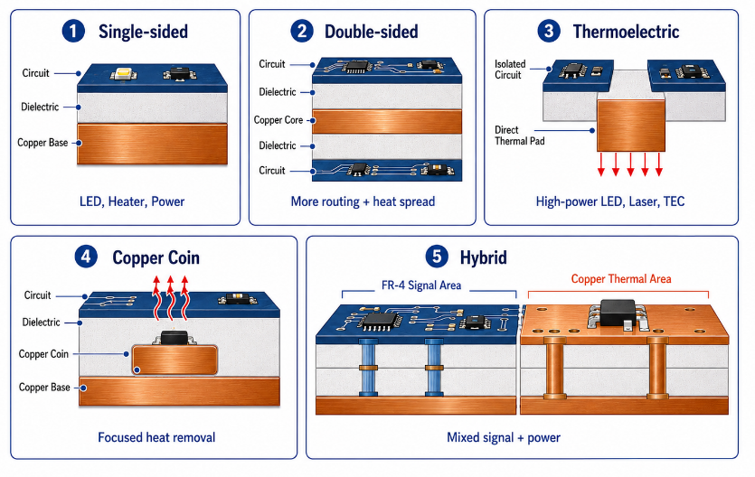
What Copper Base PCB Stack-Up Structures Are Used for Medical Diagnostic Devices?
Copper substrate stack-up should match power density, insulation needs, routing space and mechanical design. A simple single-sided structure may be enough for LED or heater modules, while double-sided or hybrid structures may be used when signal routing and thermal control must be combined.
| Type | Structure | Use Case |
|---|---|---|
| Single-sided | Circuit / dielectric / copper base | LED, heater, power module |
| Double-sided | Circuit / dielectric / copper core / dielectric / circuit | More routing and heat spreading |
| Thermoelectric separation | Direct thermal pad and isolated circuit | High-power LED, laser, TEC |
| Copper coin | Local copper insert under hot spot | Focused heat removal |
| Hybrid | FR-4 signal area plus copper thermal area | Mixed signal and power design |
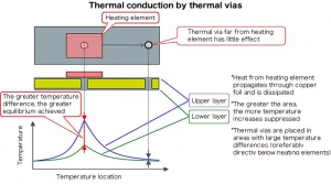
How to Design the Thermal Path in Copper Base PCB?
Thermal path design should follow the real heat movement inside the device. The goal is to move heat from the component to the copper base, then to the chassis, heatsink, airflow or metal enclosure. A complete thermal path is more important than simply choosing a thick copper substrate.
Step 1: Confirm the main heat source
Identify LEDs, MOSFETs, TEC drivers, heater circuits, power ICs and motor drivers before layout. These parts should be treated as thermal design starting points, because their heat directly affects device stability.
Step 2: Place hot components near the heat-spreading area
Keep high-power components close to the copper base contact area, screw mounting area or chassis contact surface. Long heat travel paths increase thermal resistance and create local hot spots.
Step 3: Increase pad and copper contact area
Use larger thermal pads, wider copper areas and proper copper balance when the component package allows it. More contact area helps heat move into the board faster and reduces temperature concentration around one pad.
Step 4: Select the right dielectric layer
The dielectric layer must provide both insulation and heat transfer. A thinner or higher-conductivity dielectric can improve heat flow, but it must still meet voltage safety, reliability and medical device insulation requirements.
Step 5: Separate heat-sensitive circuits
Keep analog circuits, sensors and optical signal areas away from power heat sources. If the board space is limited, use spacing, copper isolation, grounding strategy and layout partitioning to reduce thermal interference.
Step 6: Design the final heat exit path
Heat should not stop inside the PCB. Plan how the copper base contacts the enclosure, heatsink, metal bracket or thermal interface material. Poor chassis contact can weaken the benefit of the copper structure.
Step 7: Verify the design by thermal simulation or prototype testing
Use thermal simulation, infrared thermal imaging or loaded prototype testing to confirm hot-spot position and temperature rise. If the heat map is uneven, adjust pad area, copper thickness, dielectric material or enclosure contact.
How to Choose Copper Thickness, Dielectric Layer and Copper Base Thickness?
Copper thickness, dielectric layer and copper base thickness should be selected according to current load, heat density, insulation voltage, mechanical strength and cost target. Thicker copper can improve current capacity and heat spreading, but it also increases etching difficulty, spacing limits and manufacturing cost.
| Item | Common Range | Focus |
|---|---|---|
| Circuit copper | 1 oz–10 oz | Current and trace width |
| Dielectric thickness | 50 μm–150 μm | Thermal resistance and insulation |
| Dielectric conductivity | 1–12 W/mK | Heat transfer and cost |
| Copper base | 0.5 mm–3.0 mm+ | Heat spreading and rigidity |
| Surface finish | ENIG, OSP, lead-free HASL | Solderability and storage |
| Finished thickness | Custom | Enclosure and assembly fit |
The right choice is not always the thickest copper. It is the structure that meets the temperature target with stable yield and controlled cost.
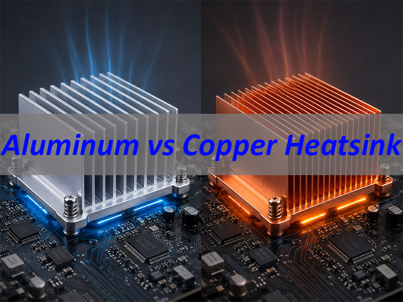
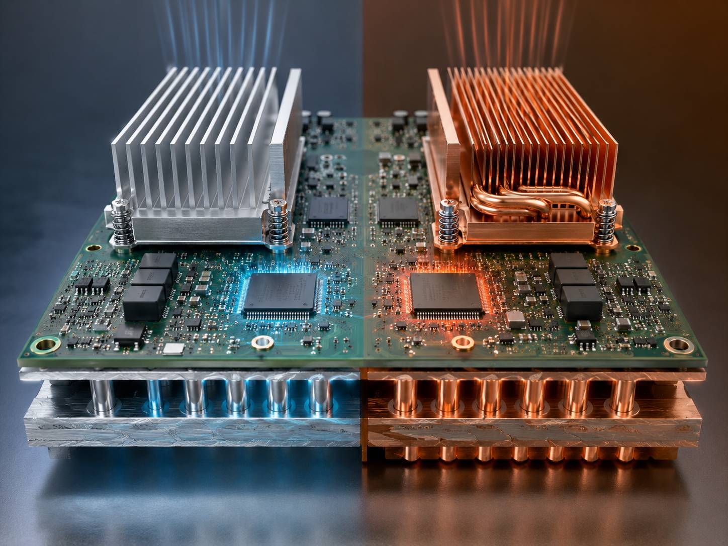
Copper Base PCB vs Aluminum PCB: Which Is Better for Medical Diagnostic Devices?
A copper substrate is better for high-power, high-current and precision thermal control modules, while aluminum PCB is better for moderate heat and cost-sensitive designs. For medical diagnostic devices, the choice should depend on thermal margin, signal stability, working time, assembly structure and budget.
| Item | Copper Base PCB | Aluminum PCB | Selection Note |
|---|---|---|---|
| Thermal performance | Higher heat spreading capacity | Moderate heat spreading capacity | Choose copper for high-density heat sources |
| Current capacity | Better for high-current paths | Suitable for medium current | Copper is better for heater, TEC and power boards |
| Temperature stability | More stable under heavy load | Acceptable for moderate load | Copper supports precision diagnostic modules |
| Mechanical strength | Strong and rigid | Good, lighter than copper | Copper works well for compact heavy-duty modules |
| Weight | Heavier | Lighter | Aluminum is better when weight is critical |
| Cost | Higher material and process cost | Lower total cost | Aluminum is better for cost-sensitive projects |
| Processing difficulty | Harder to drill, route and etch | Easier to process | Copper needs stronger process control |
| Fine line capability | More difficult with thick copper | Easier in many common structures | Review DFM before using dense circuits |
| Heat source type | Localized high-power components | Distributed moderate heat | Copper fits concentrated heat better |
| Medical application fit | Optical, TEC, heater, power, motor driver | General thermal boards and low-risk modules | Match material with risk level |
| Reliability margin | Higher when designed correctly | Good for normal thermal load | Copper gives more margin for long operation |
| Typical limitation | Higher cost and heavier weight | Lower thermal ceiling | Select based on performance target, not price alone |
For optical detection, PCR heating, TEC control, laser diode driving and compact power modules, a copper substrate usually provides better safety margin. For simple control boards, low-power LED boards or moderate thermal loads, aluminum PCB may be enough and more economical.
What Design Factors Affect Copper Base PCB Reliability in Medical Equipment?
Reliability depends on how the copper base PCB handles heat, expansion, insulation, soldering and repeated operation. Medical diagnostic equipment often runs for long periods, so small thermal stress may gradually become solder cracks, dielectric damage or electrical instability.
Key reliability factors include:
- CTE matching between copper base, dielectric, copper circuit and components.
- Dielectric breakdown strength for insulation and safety margin.
- Copper balance to reduce bow, twist and internal stress.
- Solder joint design for heavy or high-temperature components.
- Via reliability when plated holes or thermal vias are used.
- Surface cleanliness to reduce leakage in sensitive circuits.
- Surface finish stability for solderability and storage life.
A reliable design should pass both electrical and thermal verification.
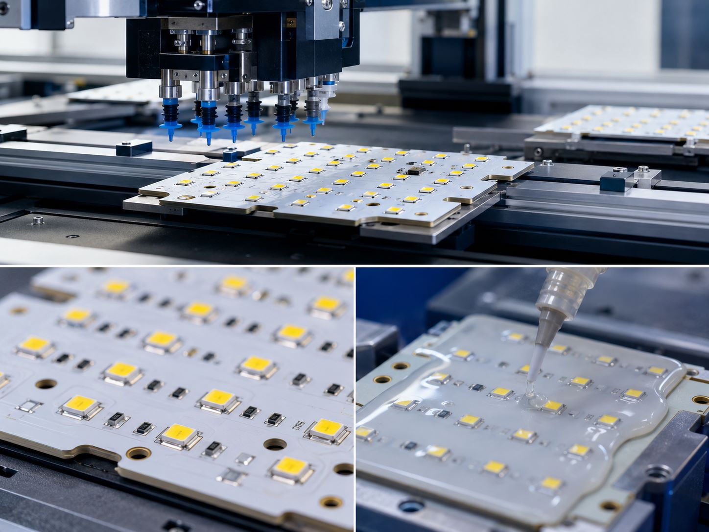
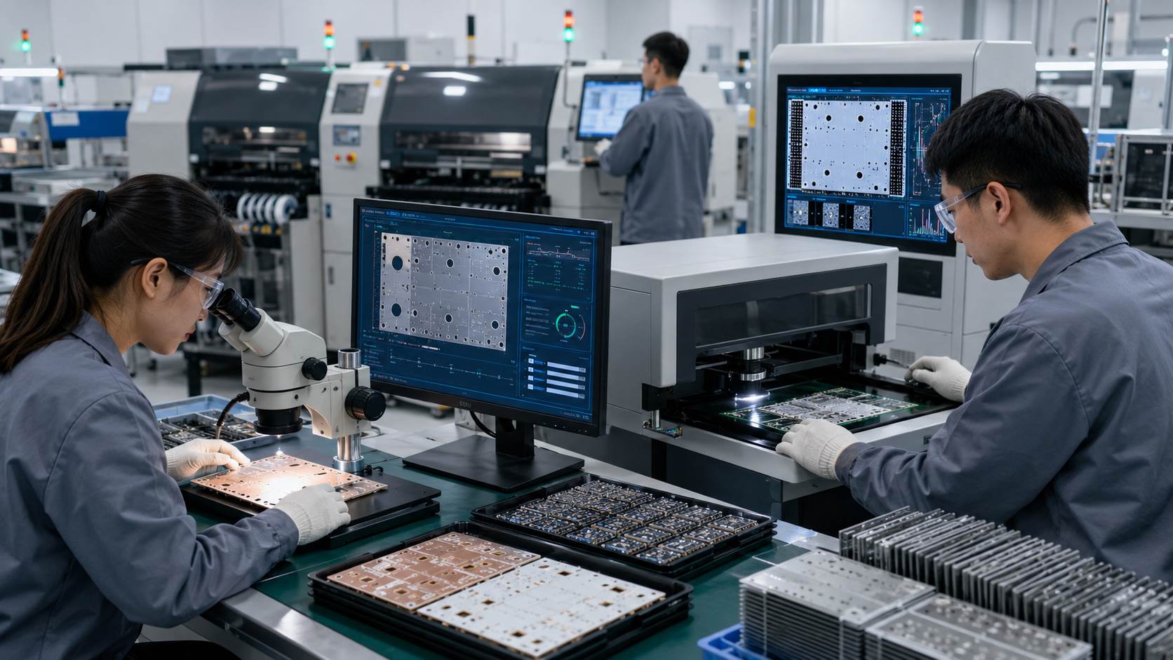
What Manufacturing Challenges Affect Copper Base PCB Quality and Cost?
Copper substrate boards are harder to manufacture than standard FR-4 boards because copper is thick, heavy and difficult to process. Etching, drilling, routing, lamination, flatness control and surface finishing all affect quality and cost.
The manufacturing process begins with stack-up and DFM review. Then the copper base is prepared, cleaned and bonded with dielectric and circuit copper. After imaging and etching, the board goes through drilling, surface treatment, solder mask, routing, electrical testing, visual inspection and final packaging.
Common cost drivers include thick copper etching, high-conductivity dielectric, tight flatness control, copper base machining, ENIG finish, small-batch setup and medical traceability requirements. Early DFM review helps reduce redesign and production risk.
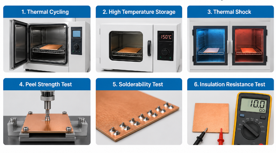
How to Test Copper Base PCB Reliability Before Medical Device Assembly?
Testing should confirm that the board can meet electrical, thermal, soldering and mechanical requirements before components are assembled. This is especially important for medical diagnostic devices because hidden thermal or insulation defects may affect long-term accuracy and reliability.
Step 1: Check the stack-up and material records
Confirm copper thickness, dielectric thickness, copper base thickness, surface finish and material batch records. This prevents wrong material selection before the board enters assembly.
Step 2: Run electrical testing
Use open, short, continuity and isolation testing to confirm that the circuit is electrically correct. This is the basic test before any thermal or assembly evaluation.
Step 3: Verify insulation performance
Use insulation resistance testing or hi-pot testing when the device has voltage isolation requirements. This helps detect dielectric weakness, contamination risk or insufficient insulation margin.
Step 4: Inspect appearance and dimensions
Check solder mask, pad shape, hole size, routing accuracy, bow, twist and surface scratches. Dimensional issues can cause poor assembly fit, unstable chassis contact or soldering problems.
Step 5: Use AOI and microscope inspection
Inspect line width, spacing, pad quality, solder mask registration and surface finish consistency. This is useful for dense diagnostic modules with small components or mixed power and signal areas.
Step 6: Perform microsection analysis when needed
Cross-section testing can check dielectric bonding, copper interface, plated hole quality and internal structure. It is useful when the board has thick copper, thermal vias or high-reliability requirements.
Step 7: Test solderability before SMT assembly
Solderability testing confirms that pads can wet properly during assembly. Poor solderability may cause weak joints, voids or unstable electrical contact after reflow.
Step 8: Use thermal imaging under load
Power the board under a controlled load and use infrared thermal imaging to locate hot spots. The test should confirm whether heat moves from the component area into the copper base as expected.
Step 9: Apply thermal cycling for reliability review
Thermal cycling helps evaluate repeated expansion and contraction stress. It is useful for heater circuits, TEC boards, optical modules and diagnostic equipment that runs for long periods.
Step 10: Review test data before assembly release
Compare all inspection results with the project requirement. Only boards with stable electrical results, acceptable thermal behavior and qualified solderability should move into medical device assembly.
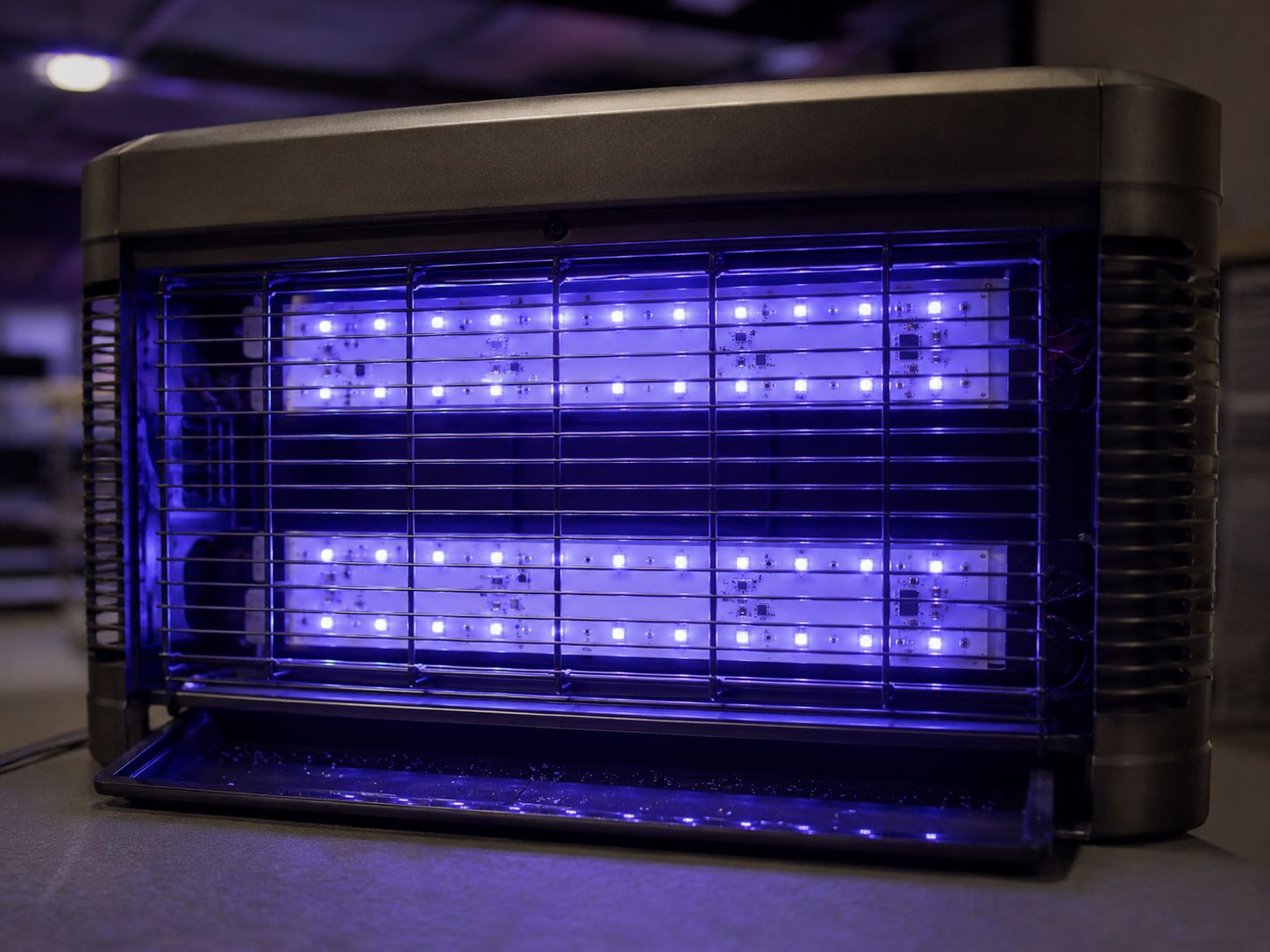
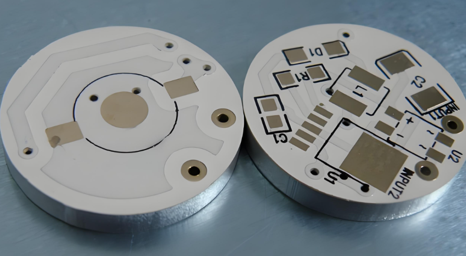
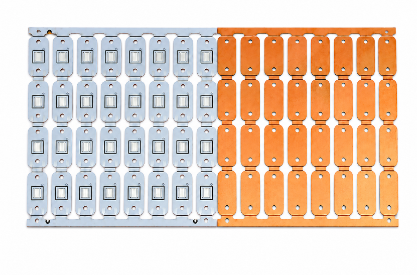
Copper Base PCB Project Case for a Medical Diagnostic Device Thermal Solution
A medical diagnostic device customer needed a compact thermal solution for an optical detection module used in laboratory testing equipment. The first FR-4 prototype could pass short functional checks, but the LED excitation area became unstable during long operation. After repeated temperature cycles, the module showed brightness drift and inconsistent signal output
Project requirements:
The customer needed better heat dissipation without increasing the module size. The board also had to support stable LED output, reliable soldering, controlled insulation, repeatable assembly and smooth fitting with the metal enclosure. The design had to be suitable for prototype verification first, then small-batch production.
Our solution:
EBest Circuit reviewed the LED pad area, current path, dielectric layer, copper thickness, copper base thickness, solder mask opening and chassis contact position. The original FR-4 structure was changed to a copper substrate structure. We increased the thermal pad area, selected a higher thermal conductivity dielectric, optimized the heat path to the enclosure and added thermal imaging to the prototype test plan.
Output result:
The updated board reduced local hot spots and improved LED output stability during continuous operation. The customer received clearer stack-up data, better inspection criteria and a more reliable prototype for medical diagnostic device validation. After verification, the project moved into small-batch production with improved thermal consistency and lower assembly risk.
What Copper Base PCB Services Can EBest Circuit Provide for Medical Diagnostic Devices?
EBest Circuit provides custom copper base PCB fabrication and PCBA support for medical diagnostic devices. As a China source factory with global delivery capability, we help customers reduce thermal risk, shorten prototype validation time and improve batch production stability.
Our main services include:
- PCB design review for copper thickness, dielectric layer, copper base thickness, insulation spacing and thermal path.
- PCB prototype support for optical detection, heater, TEC control, power and high-current medical modules.
- Mass production support with stable manufacturing capability for repeat orders.
- Component sourcing to help overseas customers reduce BOM purchasing pressure.
- PCB assembly support for medical diagnostic PCBA projects.
- Thermal path optimization from components to copper base, chassis, heatsink or enclosure.
- Quality inspection including electrical test, AOI, dimensional check, solderability review and thermal inspection.
- Traceability control for material batch, production lot and inspection records.
Why Choose EBest Circuit as Copper Base PCB Manufacturer?
EBest Circuit was founded in 2006 and has over 20 years of PCB manufacturing experience. We provide one-stop support from PCB design, prototype and mass production to component sourcing and PCB assembly.
Customers choose us because we provide:
- One-stop PCB and PCBA service
Customers can manage design review, fabrication, sourcing, assembly and inspection through one supplier. - Lower prototype risk
We review stack-up, copper thickness, dielectric layer, pad design and thermal path before production to reduce redesign and rework. - Better thermal reliability
We support copper base PCB solutions for LED excitation, PCR heating, TEC control, heater circuits, motor drivers and power modules. - Stable production capability
Our monthly production capability reaches about 260,000 square feet, supporting prototype, small batch and repeat production. - Quality system support
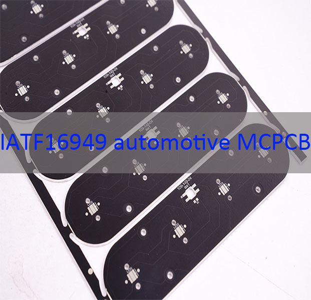
EBest Circuit holds ISO 9001:2015, ISO 13485:2016, IATF 16949, AS9100D, UL, RoHS and REACH certifications. - China source factory advantage
Customers can get custom manufacturing, flexible order support, global delivery and better cost control without unnecessary middleman layers.
For medical diagnostic device projects, EBest Circuit helps customers improve thermal stability, assembly yield, quality traceability and long-term supply reliability.
FAQs About Copper Base PCB for Medical Diagnostic Devices
Q1: When should a medical diagnostic device use a copper substrate instead of FR-4?
A1: A copper substrate should be considered when the module has high heat density, high current or strict temperature stability requirements. Common examples include LED excitation, TEC control, heater circuits and power modules. If FR-4 causes hot spots, signal drift or unstable output, a copper thermal structure can provide better reliability margin.
Q2: Is copper substrate necessary for every IVD analyzer board?
A2: No. Low-power control boards, communication boards and simple signal boards may still use FR-4. Copper substrate is mainly used in IVD modules where heat affects performance, such as heater boards, optical detection boards, motor drivers and compact power circuits. The material should be selected according to heat load and accuracy risk.
Q3: What affects the cost of a copper substrate PCB?
A3: Cost is affected by copper thickness, copper base thickness, dielectric thermal conductivity, board size, surface finish, routing difficulty, testing scope and order quantity. Thick copper, ENIG finish, tight flatness control and medical traceability can increase cost. Early DFM review helps control unnecessary process complexity.
Q4: Can copper substrate improve optical detection stability?
A4: Yes. Optical modules often use LEDs, laser diodes or excitation sources that are sensitive to temperature. Better heat spreading can reduce brightness drift, wavelength shift and local overheating. For fluorescence detection or optical sensing, stable temperature helps improve signal consistency during long operation.
Q5: What dielectric layer is suitable for medical diagnostic thermal boards?
A5: The dielectric layer should balance thermal conductivity and insulation strength. A high-conductivity dielectric improves heat transfer, while proper thickness maintains electrical safety. For medical diagnostic modules, selection should consider operating voltage, heat density, creepage, clearance and reliability testing, not only the thermal conductivity value.
Q6: Does thicker copper always mean better thermal performance?
A6: Not always. Thicker copper can improve current capacity and lateral heat spreading, but it also increases etching difficulty, spacing limits, weight and cost. The best design is based on actual current, temperature rise, component layout and production yield. Excessive copper thickness may create manufacturing risk without clear benefit.
Q7: Can copper substrate replace heatsinks or fans?
A7: It may reduce heatsink size or fan load in some compact modules, but it cannot replace the full cooling system in every case. Heat still needs to leave the PCB through the chassis, heatsink, airflow or enclosure. A complete system-level thermal path is required for stable long-term performance.
Q8: What tests should buyers request before medical device assembly?
A8: Buyers should consider electrical testing, insulation resistance testing, solderability testing, AOI, dimensional inspection, thermal imaging and microsection analysis when needed. For high-reliability modules, thermal cycling can also be added. The test plan should match the device risk level and working environment.
Q9: Can copper substrate boards support SMT assembly?
A9: Yes. Copper substrate boards can support SMT assembly, but the process should control solder paste volume, pad design, reflow profile, board flatness and component placement. Heavy copper and metal substrate structures may change heat absorption during reflow, so assembly parameters should be reviewed before batch production.
Q10: What files are needed for a copper substrate PCB quotation?
A10: Buyers should provide Gerber files, BOM, stack-up requirements, copper thickness, dielectric layer target, copper base thickness, surface finish, board quantity, assembly needs and test requirements. If the board is used in medical diagnostic equipment, traceability and inspection requirements should also be confirmed early.
Q11: How can buyers reduce risk before mass production?
A11: Start with prototype validation, then review thermal images, assembly yield, solder joint quality and electrical stability under load. Do not move directly to mass production before confirming the heat path and manufacturing tolerance. A small pilot run helps verify repeatability, test criteria and process stability.
Conclusion
A copper substrate board is a practical thermal solution for medical diagnostic devices when heat affects test accuracy, optical stability, current reliability or service life. The key selection point is not only the metal base material, but the full structure: copper thickness, dielectric layer, thermal path, enclosure contact, assembly process and reliability testing.
For procurement, buyers should confirm thermal targets, stack-up requirements, testing scope, traceability and assembly details before ordering. EBest Circuit provides custom copper substrate PCB fabrication and PCBA support from China for global medical diagnostic device projects. Send your Gerber files, BOM, stack-up target and thermal requirements to sales@bestpcbs.com for a project quotation.