





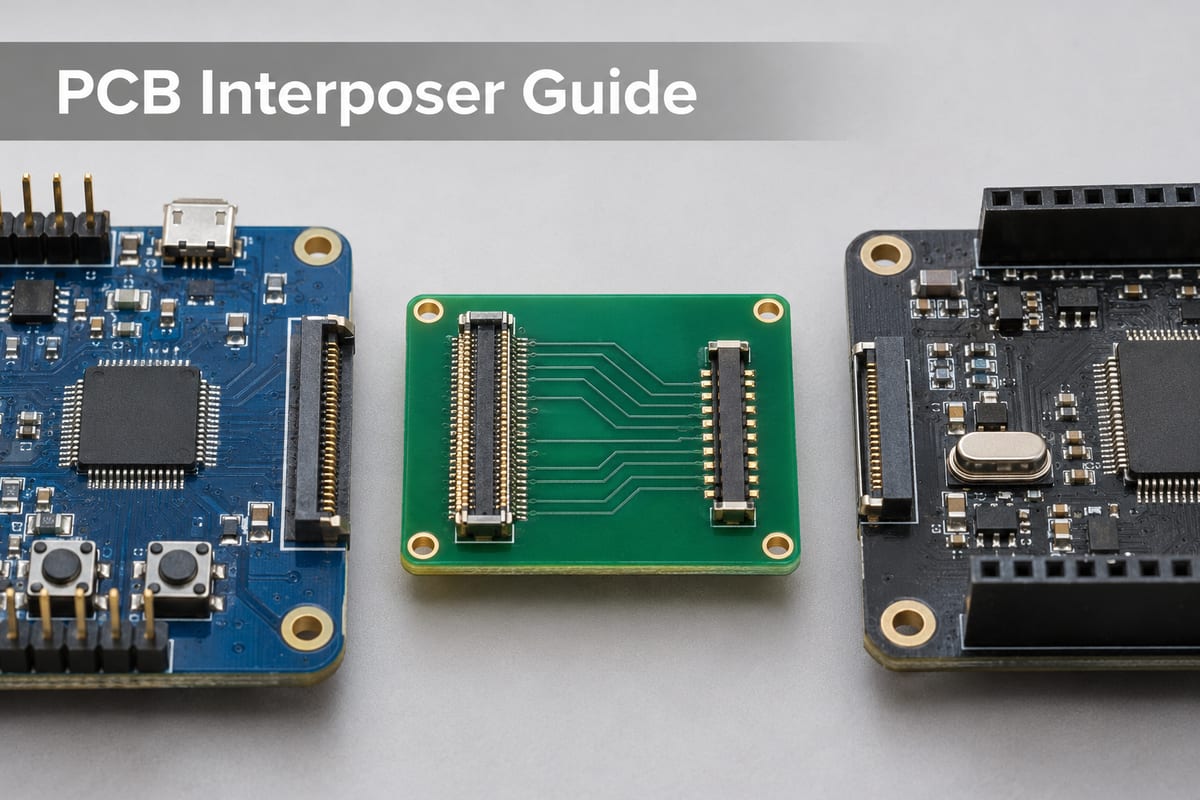
A PCB interposer is a small circuit board placed between two parts of a system to make their connections usable together. A passive interposer can move a signal to a different pin or adapt connector spacing, but it does not convert voltage levels or protocols. Before applying power, verify which pin connects to which, which side each connector drawing shows, and what voltage and direction each signal expects.
Imagine an engineer connecting a sensor daughterboard to a controller for the first time. Both connectors have four pins, but the supply pin is in a different position on each. A straight-through adapter could put power on a signal. A pin-by-pin map prevents that mistake before the boards are even plugged in.
What a PCB Interposer Does
Think of it as a short, fixed wiring harness built on a small board. Its copper paths can join connectors with different layouts, bring out test points or split selected connections into a laboratory fixture. The term can also refer to a much smaller structure inside a semiconductor package. This guide covers board-level prototype adapters, not chip-package design. For stackup, routing and fabrication considerations, see the PCB interposer design overview.
Why Matching Pin Counts Do Not Prove Compatibility
A connector’s pin count describes how many positions it has, not what those positions do. Two four-pin interfaces can disagree on the location of power and ground, the direction of the signals, and the permitted voltages. Read the board documentation at both ends; do not wire by position alone unless the functions, directions and operating conditions agree.
When to Use a Passive Board, Cable or Active Adapter
Choose the simplest connection that satisfies the electrical and mechanical requirements, not just the one that looks neatest.
| Option | Use it when |
| Passive PCB interposer | The interfaces are electrically compatible but need fixed remapping or a different footprint. |
| Cable harness | The parts need physical separation or flexible positioning, and the electrical path permits it. |
| Active adapter | The design needs a deliberate level, direction or protocol conversion. |
Analog Devices’ demonstration-platform description gives an example of using an intermediate board between a controller and a daughterboard. It does not imply that an adapter for one platform fits a different connector family.
Detailed Interface Parameters to Record
Start with the exact connector part number and hardware revision on each side. Pitch is the center-to-center distance between adjacent contacts; it is not the width of the connector body. For a concrete example, the ADRV-DPD1 Rev. A guide describes a 100-way interface with 0.8 mm pitch. That example describes that platform, not a default for interposers.
| Parameter | What to verify |
| Pitch and contact count | Read the dimensioned drawing for each mating part; compare both rows if applicable. |
| Voltage and direction | Check supply range, input/output roles and logic thresholds for the actual boards. |
| Stack height | Use the specified mated connector pair and include components, spacers and nearby walls. |
| Current and routing | Confirm contact and board requirements for the power paths; do not infer them from pitch. |
Read Pin 1 From the Correct View
A mating-face drawing shows the connector from the side where it plugs in. A board-side or solder-side view may appear mirrored. Label the view on both drawings and match pin 1 and the key to the installed position. Trace through the actual mating pair. If you cannot identify the orientation from the drawing and board markings, stop before making the map.
Build a Pin Map Before Routing
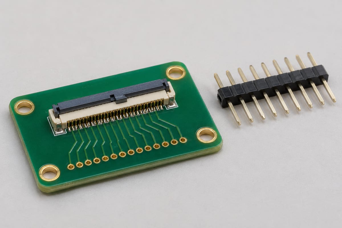
Write one row per physical contact. Include both connector designators, the contact numbers and the function of the connection. This invented example assumes both boards already support the same 3.3 V supply and the same logic interface; it is not the pinout of an actual product.
| Controller | Sensor |
| J1.1: supply out | J2.3: supply in |
| J1.2: ground | J2.4: ground |
| J1.3: command out | J2.1: command in |
| J1.4: response in | J2.2: response out |
In the example, a straight-through link would send the supply from J1.1 to J2.1, the command input. The correct path is J1.1 to J2.3. Check this row independently before relying on all the signal connections.
Check Supply Direction and Unused Pins
Identify which board supplies power and whether either can be powered separately. Connecting two outputs on the same adapter trace can create a conflict even when the labels match. Handle unused and reserved contacts according to the device documentation. Do not tie a contact to ground merely because its function is not obvious.
Keep the Signal and Its Return Path Together
Signals need a return path. An adapter adds length and connectors, so its effect can matter for fast edges, differential signals or sensitive analog paths. A connection that passes a continuity check can still distort a signal. For such interfaces, carry forward the documented routing and return-path requirements and validate the assembled channel rather than assuming a short adapter is invisible.
Check Stack Height With Both Boards Mated
Verify the adapter in the real mounting orientation. Check tall parts, cable exits, insertion direction and screw locations. A mechanically compatible footprint still needs the correct mating connector and height. Do not rely on plugging two loose boards together by hand as evidence that the stack will assemble inside its intended enclosure.
Verify the Unpowered Board Against the Map
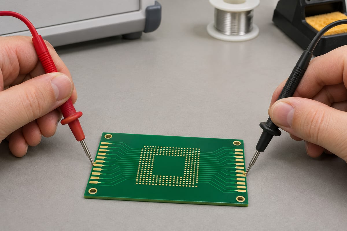
With the passive adapter disconnected and unpowered, verify each intended connection and check that unrelated contacts are not shorted. Use accessible test points and take care not to bridge adjacent pins with a probe. Cross-check pin 1, ground and each supply path first. Record the measured path against the map instead of trusting a single continuity beep.
Power Up Only After Mechanical and Electrical Checks Agree
For a documented low-voltage prototype, use its approved supply setup and initial check sequence. Confirm the intended rail at the receiving side before attaching expensive or sensitive hardware where the design allows that check. Stop if the current or voltage falls outside the expected range, a connector is reversed, or the pin map is unresolved. Continuity alone is not a power-up approval.
Make the Adapter Repeatable
Save the pin map with the schematic, board revision, connector drawings and test record. Mark orientation on the assembled unit where it can be seen before mating. For a Best Technology fabrication discussion, share the released stack, connector drawings and interface requirements with sales@bestpcbs.com. For a high-frequency transition, also review the RF via and return-path guide.
FAQ
Is a breakout board the same as an interposer?
A breakout typically makes otherwise hard-to-reach contacts accessible. An interposer sits between two interfaces, but it may also include breakout pads. Judge the board by the actual connections and purpose. Do not assume a breakout pad is isolated from the through path unless the schematic says so.
Can a passive interposer connect 5 V signals to 3.3 V inputs?
It cannot reduce the logic level by remapping pins. Check the receiving device’s documented input requirements and tolerance, and use a validated translation circuit if needed. A printed voltage label or common ground does not make an incompatible signal safe to connect to the receiving board.
Why does pin 1 look reversed on one drawing?
The drawings may be taken from opposite sides. Match each documented view to the mounted part, then follow the numbering through the mating pair. Use keying and physical pin markings as independent checks; do not apply a mirror operation simply because a drawing looks unfamiliar.
Can I connect all ground pins together?
Only where the interface definition calls for a common ground. Some systems distinguish reference, shield and isolated returns. Use the system documentation to establish which connections are allowed. Verify the finished return path against both the schematic and the intended enclosure or chassis connection.
Do I need a multilayer adapter?
Not always. A simple, slow interface may fit on fewer layers if routing and the return path are adequate. A dense or electrically demanding interface may need more routing space or a continuous reference plane. Choose the layer structure after reviewing the actual connections, not from the word interposer.
What if the connector mates but the signals are wrong?
Disconnect power and compare the two connector views, board revisions and pin functions. Check the manufactured adapter against the intended map before swapping wires or changing firmware. A connector that fits mechanically can still connect the wrong nets, so a successful mate is not proof of compatibility.
Can a long breakout stub affect a fast link?
It can. A branch attached to a fast signal creates another path that may disturb the waveform. The impact depends on the edge rate, geometry and load. Validate the full channel with the intended fixture and avoid treating a probe pad as electrically harmless in every design.
What belongs in a first-article check?
Check both part numbers, orientation, mated height, supply and ground mapping, intended connections and unintended shorts. Then use the approved electrical bring-up plan for the actual interface. Record which revision was checked so a later connector or layout change does not silently inherit the earlier result.
You may also like



Tags: Board Connectors, PCB Interposer, PCB prototyping, Pin Mapping