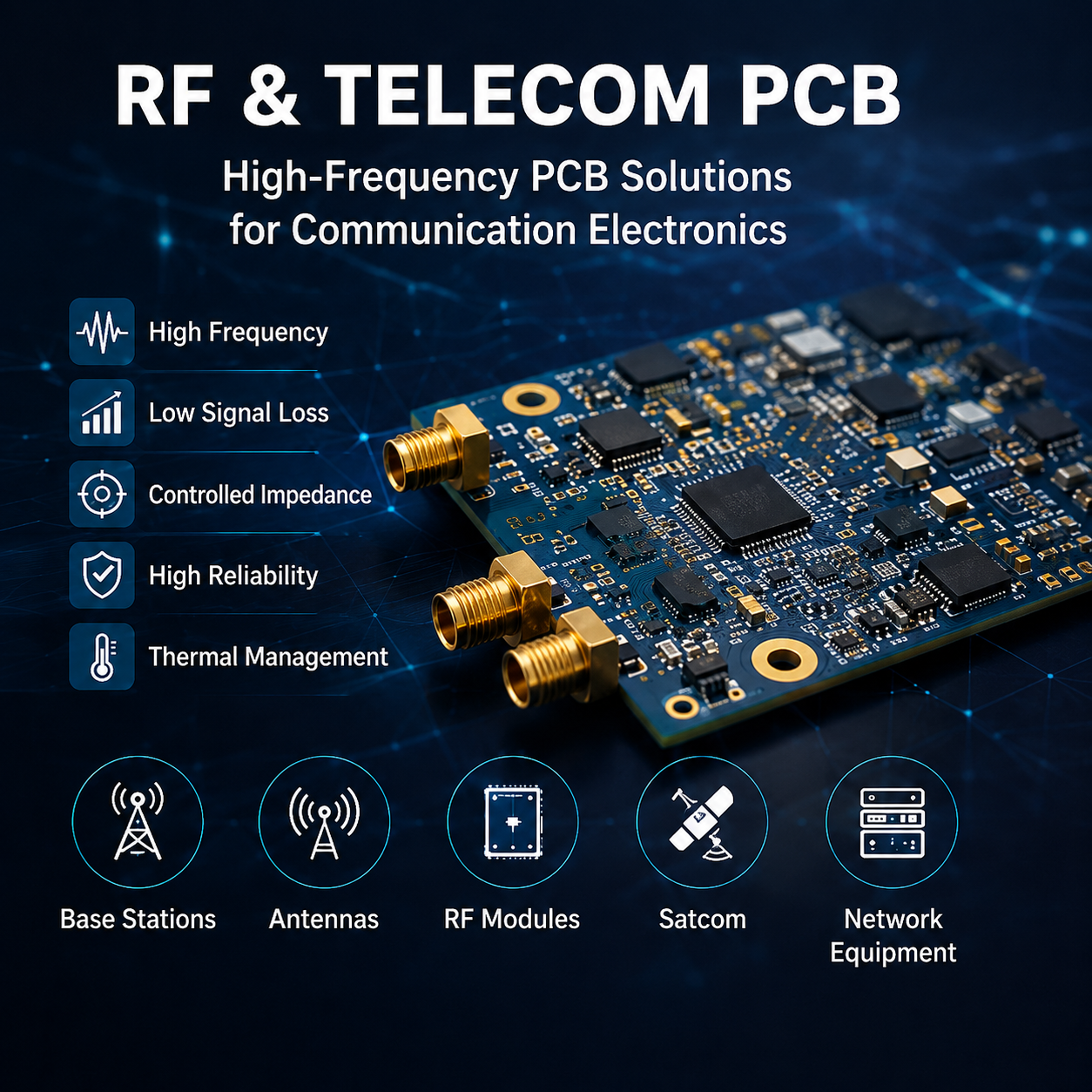
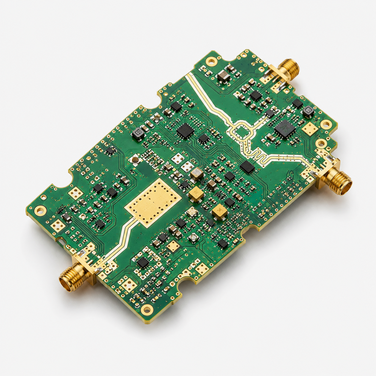
RF & Telecom electronics depend on stable signal transmission. At high frequencies, small changes in material, dielectric thickness, copper roughness, impedance, stack-up, or surface finish can affect circuit performance. Because of this, RF & Telecom PCB manufacturing requires more than standard PCB fabrication. It needs suitable materials, controlled impedance, precise stack-up management, reliable testing, and engineering review before production.
EBest Circuit supports RF and telecom PCB projects that require high-frequency materials, controlled impedance, multilayer stack-up control, thermal management, PCB assembly, and project documentation. Our capabilities include RF PCB, high-frequency PCB, HDI PCB, rigid-flex PCB, heavy copper PCB, metal core PCB, ceramic PCB, multilayer PCB, and PCBA services.
From RF PCB prototypes to telecom batch production, our engineering and manufacturing teams help customers review design feasibility, reduce manufacturing risks, and build reliable circuit boards for communication electronics.
Why RF & Telecom PCB Projects Need More Than Standard PCB Manufacturing?
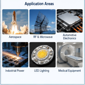
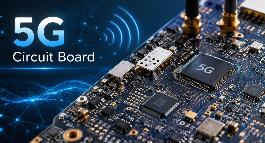
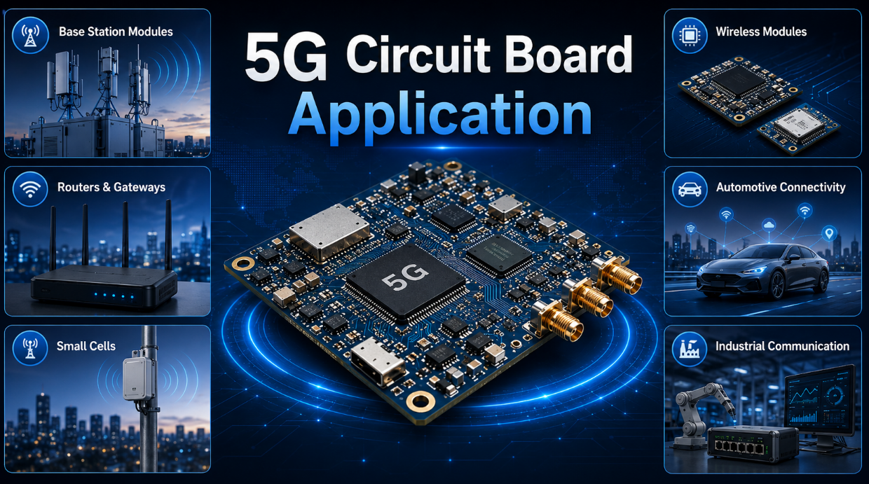
RF & Telecom PCB refers to printed circuit boards used in radio frequency and communication electronics. These boards are commonly found in wireless communication products, antenna systems, RF front-end modules, radar electronics, satellite communication equipment, network devices, optical communication systems, and telecom infrastructure.
Unlike standard PCBs, RF and telecom PCBs must support stable signal transmission. At higher frequencies, a PCB trace is not just a copper connection. It acts as a transmission line. Its width, spacing, copper thickness, dielectric thickness, material properties, reference plane, and surface finish can all influence signal behavior.
This is why RF & Telecom PCB projects need a manufacturer with high-frequency PCB experience, not only a supplier that can build basic boards.
Customers usually need more than open and short testing. They may need controlled impedance, low signal loss, stable stack-up, consistent materials, impedance test reports, PCBA support, and clear production documentation.
At EBest Circuit, RF and telecom PCB manufacturing is handled as an engineering-driven process. We review material selection, stack-up, impedance targets, copper thickness, via structures, thermal paths, and assembly requirements before production when needed.
What Makes RF & Telecom PCBs Difficult to Build?
RF and telecom PCBs are difficult to build because small production variables can affect performance. A board may pass basic electrical testing but still perform poorly in an RF circuit if impedance, material loss, or signal transition is not controlled.
- High-frequency signals are sensitive to dielectric constant and dissipation factor. If the material is not suitable for the operating frequency, signal loss may increase.
- Controlled impedance is also critical. RF circuits often use 50-ohm single-ended impedance, while high-speed telecom circuits may require 90-ohm or 100-ohm differential impedance. Impedance can shift if trace width, spacing, dielectric thickness, or copper thickness is not controlled.
- Stack-up design affects return paths, shielding, crosstalk, and signal stability. RF layers need proper reference planes and stable dielectric spacing. Poor stack-up planning may cause signal reflection, EMI issues, or inconsistent performance.
- Via design is another key factor. Via transitions, via stubs, ground vias, and layer changes can affect RF and high-speed signals. The design must balance electrical performance and manufacturability.
- Surface finish and copper profile may also influence high-frequency behavior. At higher frequencies, signal current tends to flow near the conductor surface, so copper roughness and surface treatment can affect loss.
Telecom equipment often needs stable performance over long operating periods. For base stations, antenna modules, RF front-end circuits, network devices, and optical communication equipment, repeatable manufacturing is as important as the first successful prototype.
Our RF & Telecom PCB Manufacturing Capabilities
EBest Circuit supports RF and telecom PCB projects across different board structures, materials, and production stages. We help customers choose suitable manufacturing solutions according to frequency, impedance target, thermal load, board size, assembly method, and production volume.
Our RF and telecom PCB capabilities include:
- RF PCB for antenna modules, RF front-end circuits, wireless communication products, and microwave systems
- High-frequency PCB using RF laminates and customer-specified high-frequency materials
- Controlled impedance PCB for RF and high-speed telecom signals
- Multilayer telecom PCB for communication equipment, network systems, and control modules
- HDI PCB for compact communication products and high-density routing
- Rigid-flex PCB for space-limited RF and telecom assemblies
- Hybrid stack-up PCB combining RF materials with FR4 or other substrates
- Heavy copper PCB for telecom power control and current-carrying circuits
- Metal core PCB for RF power modules and thermal management applications
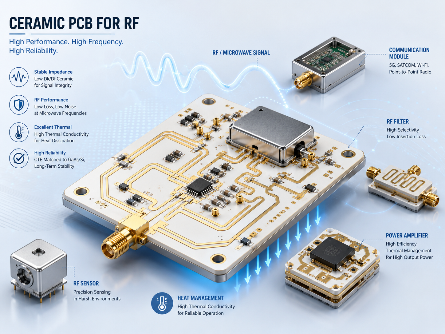
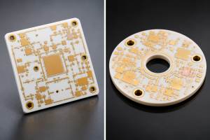
- Ceramic PCB for high-power, high-heat, and dimensionally stable electronic modules
- PCBA service for PCB fabrication, component sourcing, SMT assembly, inspection, testing, and box-build support
Different communication products require different PCB structures. An antenna module may require low-loss RF laminate and controlled impedance. A telecom control board may need multilayer FR4 with impedance control. A compact communication device may require HDI or rigid-flex PCB. A power amplifier module may need heavy copper, metal core, or ceramic PCB for heat dissipation.
Our engineering team can review the design and suggest a practical manufacturing route before production.
What Types of PCBs Are Used in RF and Telecom Equipment?
RF and telecom equipment can use different PCB types depending on frequency, signal speed, power level, mechanical layout, heat dissipation, and cost target.
RF PCB is used for radio frequency circuits, including antenna modules, RF front-end boards, wireless communication products, microwave systems, and signal transmission modules. RF PCB manufacturing requires careful control of material properties, impedance, dielectric spacing, copper thickness, and surface quality.
High-frequency PCB is used when the circuit works at higher frequencies and needs lower signal loss. These boards often use RF laminates, PTFE-based materials, ceramic-filled materials, or other high-frequency substrates. They are common in radar, microwave communication, satellite communication, and advanced wireless systems.
Telecom equipment often uses multilayer PCBs because the design may include RF signals, high-speed digital signals, power distribution, grounding, shielding, and control circuits. A stable multilayer stack-up helps improve routing density, signal integrity, and EMC performance.
Controlled impedance PCB is widely used in RF and telecom electronics. The board must be manufactured according to defined impedance targets. This requires coordination between design, material selection, stack-up, trace geometry, copper thickness, and manufacturing tolerance.
HDI PCB is suitable for compact telecom products, RF modules, IoT communication devices, and high-density control systems. Microvias, blind vias, buried vias, and fine lines help reduce board size while supporting complex routing.
Rigid-flex PCB can reduce connectors, save space, and improve mechanical reliability. It is suitable for compact communication equipment, antenna systems, portable RF modules, and assemblies where cable reduction is important.
Heavy copper PCB is used for power supply sections, current-carrying circuits, and telecom power modules. It improves current capacity and supports better heat spreading in power areas.
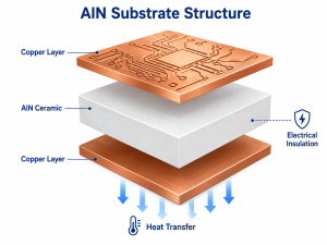
Metal core PCB helps transfer heat away from power components. Aluminum base and copper base PCBs can be used in RF power modules, LED communication modules, and telecom thermal management designs.
Ceramic PCB offers high thermal conductivity, dimensional stability, and electrical insulation. It can be used in high-power RF modules, microwave circuits, laser communication modules, and high-heat telecom applications.
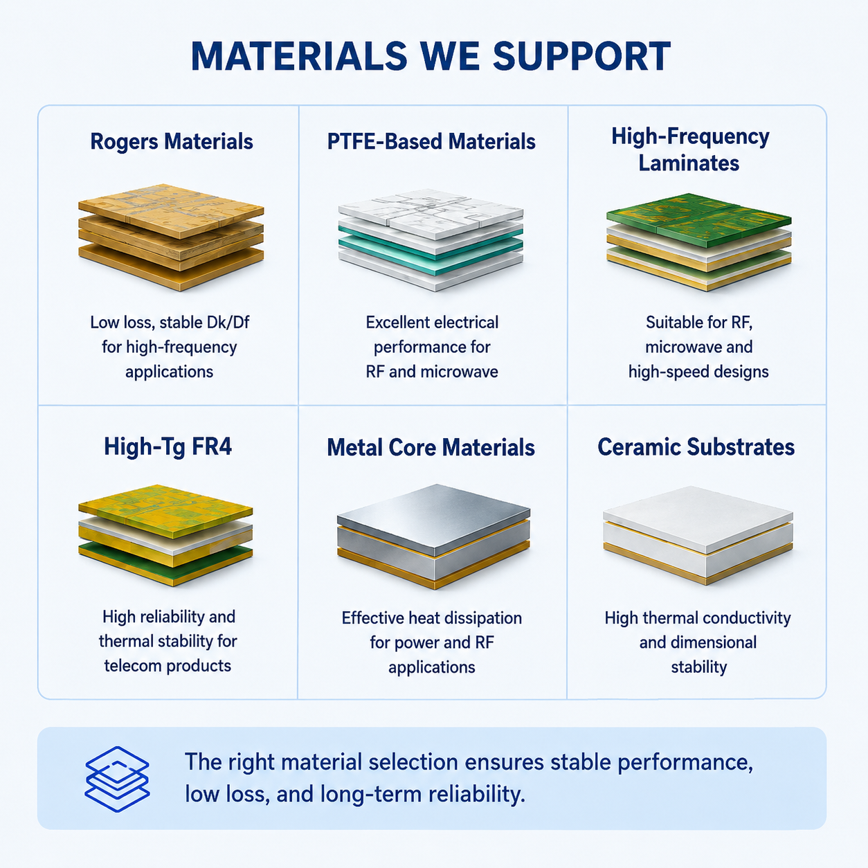
Materials We Support for RF & Telecom PCB Applications
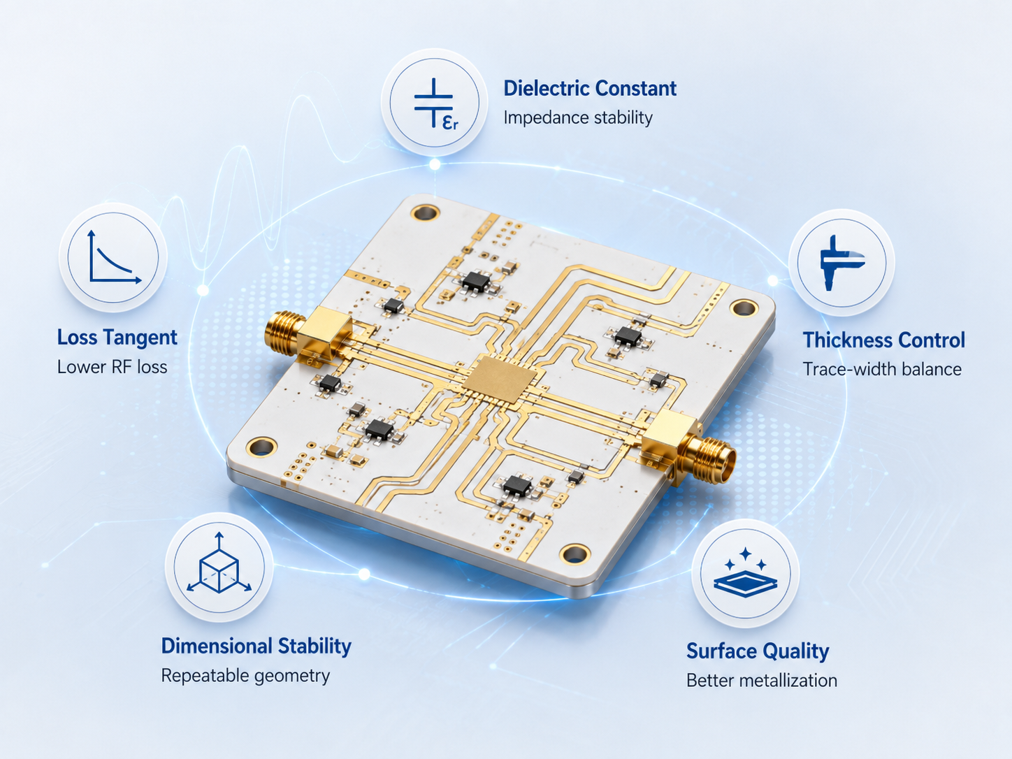
Material selection is one of the most important decisions in RF and telecom PCB manufacturing. The material affects impedance, signal speed, insertion loss, thermal behavior, dimensional stability, and cost.
EBest Circuit can support RF and telecom PCB projects using different material options based on customer requirements.
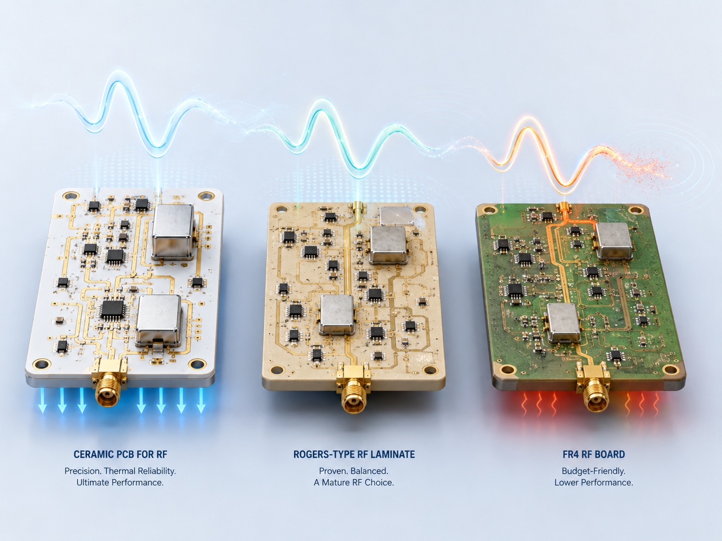
High-frequency laminates are used when low loss and stable electrical performance are required. They are suitable for RF circuits, microwave circuits, antenna boards, satellite communication modules, and radar-related applications.
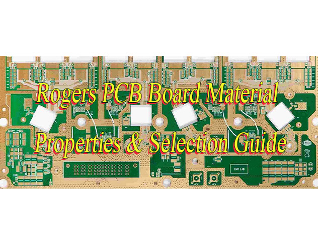
Rogers materials are commonly used in RF and microwave PCB applications because they offer more stable electrical properties and lower loss than standard FR4 in many high-frequency designs. They are often selected for antenna systems, RF modules, radar boards, and telecom equipment.
PTFE-based materials are widely used in RF and microwave circuits. They support low-loss signal transmission and stable dielectric behavior, making them suitable for high-frequency applications.
Not every telecom PCB requires RF laminate across the whole board. Some communication products use high-speed FR4 or high-Tg FR4 for digital, control, or power sections, while RF areas use special high-frequency materials.
Hybrid stack-up is useful when a design combines RF circuits with standard digital or power circuits. It can help balance performance and cost. However, hybrid material construction needs careful lamination control because different materials may have different thermal expansion and bonding behavior.
Aluminum and copper base materials can be used when RF or telecom modules generate heat. Metal core PCB helps improve heat transfer from power devices and supports stable operation in thermal-sensitive designs.
Ceramic substrates are suitable for compact, high-power, and high-heat RF or telecom modules. They provide good thermal conductivity, electrical insulation, and dimensional stability.
Material selection should be based on operating frequency, impedance target, insertion loss requirement, board thickness, thermal load, cost target, and production volume.
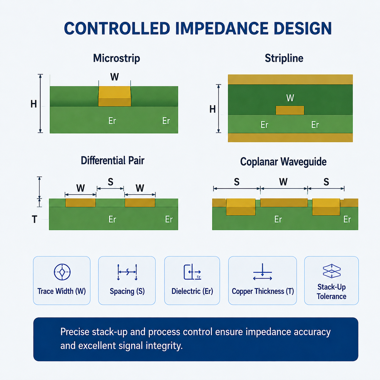
Controlled Impedance and Stack-Up Engineering Support
Controlled impedance is central to RF & Telecom PCB manufacturing. Many RF circuits use 50-ohm impedance. High-speed telecom circuits may require 90-ohm or 100-ohm differential impedance. Other values may also be used depending on the design.
Impedance is affected by:
- Trace width
- Trace spacing
- Copper thickness
- Dielectric thickness
- Dielectric constant
- Solder mask thickness
- Reference plane distance
- Stack-up structure
- Manufacturing tolerance
If these factors are not controlled, the board may have impedance deviation. This can cause signal reflection, signal loss, timing issues, EMI problems, or unstable RF performance.
Our engineering team can review your stack-up before production. This review may include dielectric thickness, copper thickness, layer arrangement, impedance targets, trace width, spacing, reference planes, solder mask influence, and impedance coupon design.
We can support different transmission line structures, including:
- Microstrip
- Stripline
- Coplanar waveguide
- Differential pairs
- RF transmission lines
- Controlled impedance signal layers
For projects that require impedance testing, we can review the test requirements and arrange impedance coupons according to the design. This helps customers confirm whether the manufactured board meets the required impedance range.
Signal Integrity, Loss Control, and RF Design Factors
RF and telecom PCB performance depends on the full signal path, including traces, vias, pads, connectors, reference planes, grounding, shielding, and layer transitions.
Insertion loss refers to signal loss through the transmission path. It can be affected by material dissipation factor, copper roughness, trace length, frequency, surface finish, and via transitions. Lower loss is important for many RF and telecom applications.
Return loss is related to signal reflection. If impedance is not well controlled, part of the signal may reflect back instead of continuing through the line. This can affect RF performance and communication quality.
Dense telecom boards may include many high-speed signals. Poor spacing, weak reference planes, or improper routing can increase crosstalk. Proper layer planning and routing rules help reduce interference.
Vias can create discontinuities in RF and high-speed paths. Via stub length, anti-pad design, ground via placement, and layer transition structure may affect signal performance.
RF circuits need stable grounding and proper shielding. Ground vias, via fences, reference planes, and shield cans may be used to reduce unwanted coupling and radiation.
Surface finish affects solderability, flatness, contact performance, and high-frequency behavior. The suitable finish should be selected according to RF performance, assembly requirements, storage needs, and customer specifications.
Many telecom products contain both RF circuits and high-speed digital circuits. These areas may have different design rules. A proper stack-up and grounding strategy can help reduce interference between functional sections.
Our team helps review manufacturability risks and production variables that may affect performance, including material selection, stack-up, copper thickness, impedance control, via structure, surface finish, and assembly feasibility.
Thermal Management for RF and Telecom Power Modules
RF and telecom PCB projects are not only about signal performance. Many communication products also generate heat. RF power amplifiers, base station modules, telecom power boards, LED communication devices, and power conversion circuits may require better thermal management.
Heat can affect component life, signal stability, solder joint reliability, and long-term product performance. If thermal paths are not designed properly, heat may concentrate around power devices.
Thermal management may involve:
- Heavy copper for higher current and heat spreading
- Thermal vias for heat transfer between layers
- Copper balancing for manufacturing stability
- Metal core PCB for heat dissipation
- Copper base PCB for stronger thermal transfer
- Aluminum base PCB for cost-effective heat dissipation
- Ceramic PCB for thermal conductivity and electrical insulation
- Component placement for shorter thermal paths
- Heat sink connection areas
- Thermal pad and solder mask opening control
EBest Circuit supports heavy copper PCB, metal core PCB, copper base PCB, aluminum PCB, and ceramic PCB for RF and telecom modules that require better heat dissipation.
For power-related telecom projects, our engineering team can review copper thickness, thermal vias, base material, heat transfer path, solder mask design, and assembly requirements before production.
Quality Control for RF & Telecom PCB Manufacturing
For RF and telecom PCB projects, quality control is not only open and short testing. It also includes stable materials, accurate stack-up, controlled impedance, plating consistency, and repeatable production.
Our quality control process can include:
- Incoming material inspection
- Engineering file review
- Stack-up confirmation
- Inner layer AOI
- Lamination process control
- Drilling inspection
- Plating thickness control
- Solder mask inspection
- Surface finish inspection
- Electrical testing
- Impedance testing when required
- Microsection analysis when required
- Final visual inspection
- Packing inspection
- Traceability documentation
For controlled impedance projects, test coupons can be used to verify impedance performance. For multilayer telecom PCBs, stable lamination and dielectric thickness control are important. For RF PCBs, material handling, surface quality, and process consistency need careful control.
For PCBA projects, additional inspection can include:
- BOM review
- Component sourcing control
- Solder paste inspection
- SMT placement inspection
- Reflow process control
- AOI inspection
- X-ray inspection for BGA or hidden solder joints
- RF connector assembly inspection
- Functional testing when required
- Conformal coating when required
- Final assembly inspection
Quality for RF & Telecom PCB manufacturing depends on correct material selection, practical stack-up, stable fabrication, controlled assembly, and clear inspection requirements.
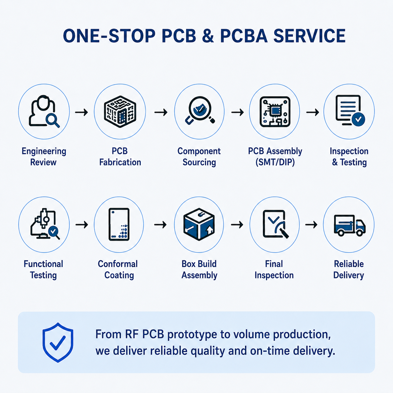
PCB Assembly Support for RF & Telecom Electronics
Many customers need more than bare PCB fabrication. RF and telecom projects may require PCB assembly, component sourcing, RF connector assembly, shield can assembly, functional testing, and box-build service.
EBest Circuit provides PCB and PCBA one-stop support to help customers reduce supplier coordination work. Customers can combine PCB fabrication, component sourcing, SMT assembly, inspection, testing, and final packaging with one team.
Our PCBA capabilities include:
- SMT assembly
- DIP assembly
- Fine-pitch component assembly
- BGA assembly
- QFN and QFP assembly
- RF connector assembly
- Shield can assembly
- Component sourcing support
- BOM review
- PCB fabrication and assembly coordination
- SPI inspection
- AOI inspection
- X-ray inspection
- Functional testing
- Conformal coating
- Box-build assembly
Assembly quality can affect RF and telecom product performance. Connector alignment, solder joint quality, shielding structure, cleaning, reflow profile, and component placement all need attention.
For projects that require testing, our team can review the customer’s functional test method before production. If special RF testing is required, we can discuss the test conditions and support production coordination based on customer specifications.
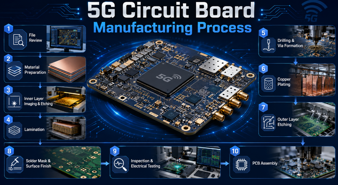
From RF PCB Prototype to Telecom Batch Production
RF and telecom projects often start with prototypes. Engineers may need to verify frequency performance, impedance, material choice, antenna behavior, thermal design, connector structure, and assembly feasibility before moving to batch production.
EBest Circuit supports customers through different project stages:
- RF PCB prototype
- Engineering sample
- Design verification build
- Small-batch production
- Pilot run
- Telecom batch production
- Repeat order manufacturing
- PCB assembly and testing
- Box-build support when required
For prototype projects, customers often need fast feedback and practical manufacturability suggestions. Our engineering team can review the design and point out issues related to material, stack-up, drill design, impedance, copper thickness, or assembly.
For batch production, customers need stable material supply, repeatable processes, controlled inspection, and clear documentation.
Because we support both prototype and production stages, customers can move from early design review to later production with better continuity.
What Files Should You Send for an RF & Telecom PCB Quote?
A complete quotation package helps our engineering team evaluate your RF & Telecom PCB project faster and more accurately. Because RF and telecom designs are sensitive to materials and stack-up, complete information helps improve quotation accuracy.
For bare PCB fabrication, please prepare:
- Gerber files
- Drill files
- Stack-up requirement
- Material brand or material type
- Target frequency if available
- Impedance requirement
- Copper thickness
- Board thickness
- Surface finish
- Solder mask requirement
- Silkscreen requirement
- Controlled impedance tolerance
- Impedance test requirement
- Special via structure requirement
- Quantity
- Expected lead time
- Testing requirement
- Special documentation requirement
For PCBA projects, please also provide:
- BOM
- CPL or pick-and-place file
- Assembly drawing
- RF connector requirement
- Shielding requirement
- Functional test instruction if available
- Programming requirement if needed
- Conformal coating requirement if needed
- Box-build documents if required
If your files are not complete, you can send the available files first. Our engineering team can help check what information is missing before quotation.
Why Choose EBest Circuit for RF & Telecom PCB Projects?
Choosing an RF & Telecom PCB manufacturer is about more than price. A supplier should be able to support material review, impedance control, stack-up engineering, thermal management, reliable manufacturing, PCBA, and technical communication.
EBest Circuit supports RF and telecom PCB projects through manufacturing experience, wide PCB capability, engineering support, quality control, and one-stop PCB assembly service.
Founded in 2006, EBest Circuit has long-term experience in PCB manufacturing and PCB assembly. We serve customers in communication electronics, industrial control, automotive electronics, medical devices, power electronics, aerospace-related electronics, and other high-reliability fields.
This experience helps us understand the requirements of RF and telecom projects, including materials, impedance, signal behavior, thermal performance, assembly quality, and production consistency.
Our capabilities include RF PCB, high-frequency PCB, controlled impedance PCB, multilayer PCB, HDI PCB, rigid-flex PCB, heavy copper PCB, metal core PCB, ceramic PCB, and PCBA.
This gives customers more flexibility when choosing the right board structure for communication equipment, RF modules, antenna systems, power boards, and high-speed telecom products.
We do not only quote from Gerber files. Our engineering team can review material selection, stack-up, impedance targets, copper thickness, via structure, RF routing risks, thermal paths, and assembly feasibility before production.
We can support RF and telecom PCB projects using customer-specified high-frequency materials and controlled impedance requirements. Our team can review dielectric thickness, trace width, spacing, copper thickness, reference planes, and impedance coupons according to project needs.
We provide PCB fabrication, component sourcing support, SMT assembly, DIP assembly, inspection, functional testing, conformal coating, and box-build support. This helps customers reduce supplier management work and improve project communication.
We support RF PCB prototypes, engineering samples, small batches, pilot runs, batch production, and repeat orders. Customers can work with one manufacturing partner from early development to later production.
Our quality management approach supports controlled manufacturing, inspection, testing, and documentation. For projects with special quality, traceability, or inspection requirements, our team can review the details before production.
RF and telecom projects often involve technical questions. Our team can communicate with customers about material options, stack-up feasibility, impedance control, testing needs, assembly risks, and delivery planning.
Frequently Asked Questions About RF & Telecom PCB Manufacturing
- What is an RF & Telecom PCB?
An RF & Telecom PCB is a printed circuit board used in radio frequency and communication electronics. Common applications include antenna modules, RF front-end circuits, wireless devices, base station equipment, radar modules, satellite communication systems, optical communication devices, and network equipment.
- What is the difference between RF PCB and standard PCB?
A standard PCB mainly provides electrical connections. An RF PCB must also control signal loss, impedance, dielectric behavior, copper quality, grounding, shielding, and signal path stability. It usually requires more careful material selection and stack-up control.
- What materials are used for RF PCB manufacturing?
RF PCB materials may include Rogers materials, PTFE-based materials, high-frequency laminates, ceramic-filled substrates, high-speed FR4, high-Tg FR4, metal core materials, and ceramic substrates. The best material depends on frequency, loss target, impedance requirement, thermal needs, cost, and production volume.
- Can you manufacture Rogers PCB?
Yes. We can support RF and high-frequency PCB projects using Rogers materials and other customer-specified RF laminates. Please send your material requirement, stack-up, Gerber files, and impedance targets for engineering review.
- Can RF PCB combine Rogers and FR4 materials?
Yes. Some RF and telecom designs use hybrid stack-up structures that combine RF materials with FR4 or other materials. This can help balance performance and cost, but it requires careful lamination and stack-up review before production.
- Why is controlled impedance important for telecom PCB?
Controlled impedance helps maintain signal stability and reduce signal reflection, timing issues, and transmission problems. In telecom PCB designs, impedance is affected by trace width, spacing, dielectric thickness, copper thickness, material properties, and reference plane design.
- What surface finish is suitable for RF PCB?
The suitable surface finish depends on RF performance, assembly method, storage requirement, solderability, and customer specification. Common options may include ENIG, immersion silver, OSP, or other finishes depending on project needs.
- Do you provide RF PCB assembly?
Yes. We provide RF and telecom PCBA services, including SMT assembly, DIP assembly, RF connector assembly, shield can assembly, component sourcing support, AOI inspection, X-ray inspection, functional testing, conformal coating, and box-build support when required.
- Can you support RF PCB prototypes?
Yes. We support RF PCB prototypes, engineering samples, small batches, pilot runs, and batch production. Our engineering team can review files before production to help reduce manufacturability risks.
- What files are needed for an RF & Telecom PCB quotation?
For PCB quotation, please send Gerber files, drill files, stack-up requirements, material requirements, impedance targets, copper thickness, board thickness, surface finish, quantity, and lead time. For PCBA quotation, please also send BOM, CPL, assembly drawings, and testing instructions if available.
Need RF & Telecom PCB Manufacturing Support?
If you are developing RF communication products, telecom equipment, antenna modules, radar electronics, wireless devices, optical communication systems, or high-speed signal boards, EBest Circuit can help review your project before production.
We support RF PCB, high-frequency PCB, controlled impedance PCB, multilayer telecom PCB, HDI PCB, rigid-flex PCB, heavy copper PCB, metal core PCB, ceramic PCB, and PCBA services for communication electronics.
Our engineering team can review your Gerber files, stack-up, material requirements, impedance targets, copper thickness, thermal needs, assembly risks, and production feasibility. Whether you need RF PCB prototypes, small-batch builds, telecom batch production, or one-stop PCB assembly, we can help you choose a practical manufacturing solution.
Send your project files and requirements to sales@bestpcbs.com. Our team will help evaluate your RF & Telecom PCB project and provide engineering support for quotation and production.