Because its special characteristics of thick film ceramic PCB, you cannot design that ceramic board following the design rule of FR4. Here are simple design guide for Thick Film Ceramic printed circuit board.
Substrate/Core raw material Thickness:
0.25mm, 0.38mm, 0.50mm, 0.63mm(standard), 0.76mm, 1.0mm, and 1.27mm (only for AIN), and special thickness such as 1.6mm, 2.0mmm, need to be customized.
Application type: SMD/SMT; Aluminum-Wire Bonding; Gold-wire bonding, Ozone plate. Please advise that information so that different material and thickness will be adopted accordingly
Conductor (metallization) layer thickness: >=10um
Minimum (Min) Trace Space/Width for volume production:0.30mm & 0.30mm, 0.20mm/0.20mm is also okay but cost will be higher, and 0.15mm/0.20mm only available for prototype.
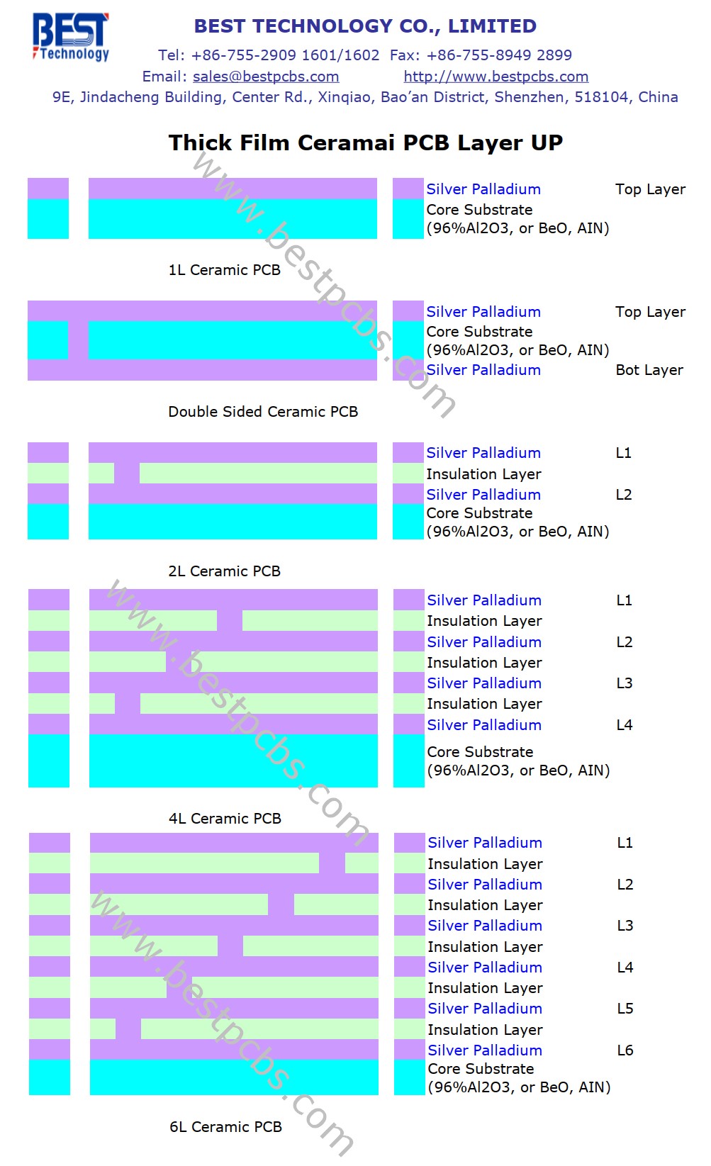
Layers Number: 1L, 2L, Double sided (with PTH), 3L~10L with or without PTH
C) Conductor Resistivity
Different conductor material has different resistivity value.
The thicker conductor thickness is, the lower resistivity value will be.
The power density for conductor itself should be limited to max 600 Watt/inch2 of conductor surface. And power density for an Al2O3 substrate should be limited to 8 Watts/in2 (for the total of all conductors on top of it)
If you have a Ag conductor line of 0.3inch long, 0.010 inch wide (=30 square (0.3/0.01)), the surface area is 0.3 x 0.01 = 0.003 in2. This means the carrying powder P is limited to 600 (power density) x 0.003 (area) = 1.8 watts.
Assume conductor resistivity is 6mOhm/sq/12.5um (ESL9562), the resistance value R = 30 sq x 6mOhm = 0.18 ohm.
Power = I2 x R, or I2 =Power/R=1.8/0.18 = 10, so the carrying current limit I = 3.16 amps. Or in a short equation: I (amps) = line width (inch) x (power density)1/2 / (sheet resistance, ohm) 1/2
If the trace keep 0.3 inch long, but change width to 0.02inch, (=15 square (0.3/0.02), the surface area is 0.3 x 0.02 = 0.006 in2. This means the carrying powder P is limited to 600 (power density) x 0.006 (area) = 3.6 watts. And resistance value for that trace will be 15 square x 6mOhm = 0.09 ohm, and then 3.6/0.09= 40, I=6.325 amps.
If the trace width keep 0.01inch, but change line to 0.6 inch long (=60 square (0.6/0.01), the surface area is 0.6 x 0.01 = 0.006 in2. This means the carrying powder P is the same as 3.6 watts. (600x0.006).
But the resistance value for that trace will change to be 60 square x 6mOhm = 0.36 ohm, and then 3.6/0.36= 10, I=3.16 amps. So you can see, it’s no useful to change the trace line.
So if you want to have bigger current, then you need to increase the width of trace.
E) Surface finishing:
For conductor is AgPd or AuPd, then surface finishing is raw material itself, no extra finishing. For Mo/Mu, then Nickel plating.
F) Bonded Resistors:
Different resistor value can be put on the same board, each different resistor period need to set up a new stencil, and can only be printed separately.
Resistor can be on the same layer/side, or different layer/side
Bonded resistor can support high temperature up to 500C;
Please advise temperature coefficient
G) Soldermask
It is glass glaze
Ceramic PCB can be either with or without soldermask
Color: transparent greenish
H)PTH (Plated Through Hole) & NPTH (Non-Plated Through Hole)
