PCB manufacturing PCB manufacturing
Home > Blog

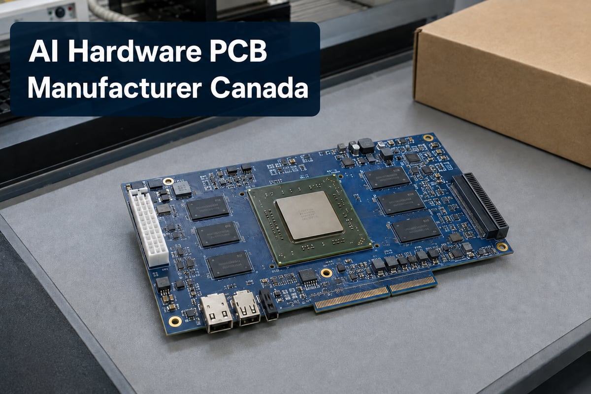
AI Hardware PCB Manufacturers in the USA: 15 Suppliers to Compare

September 4th, 2026

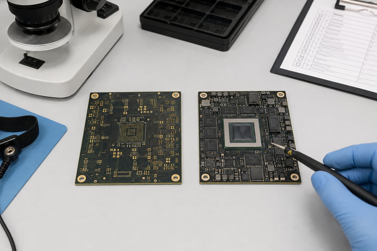
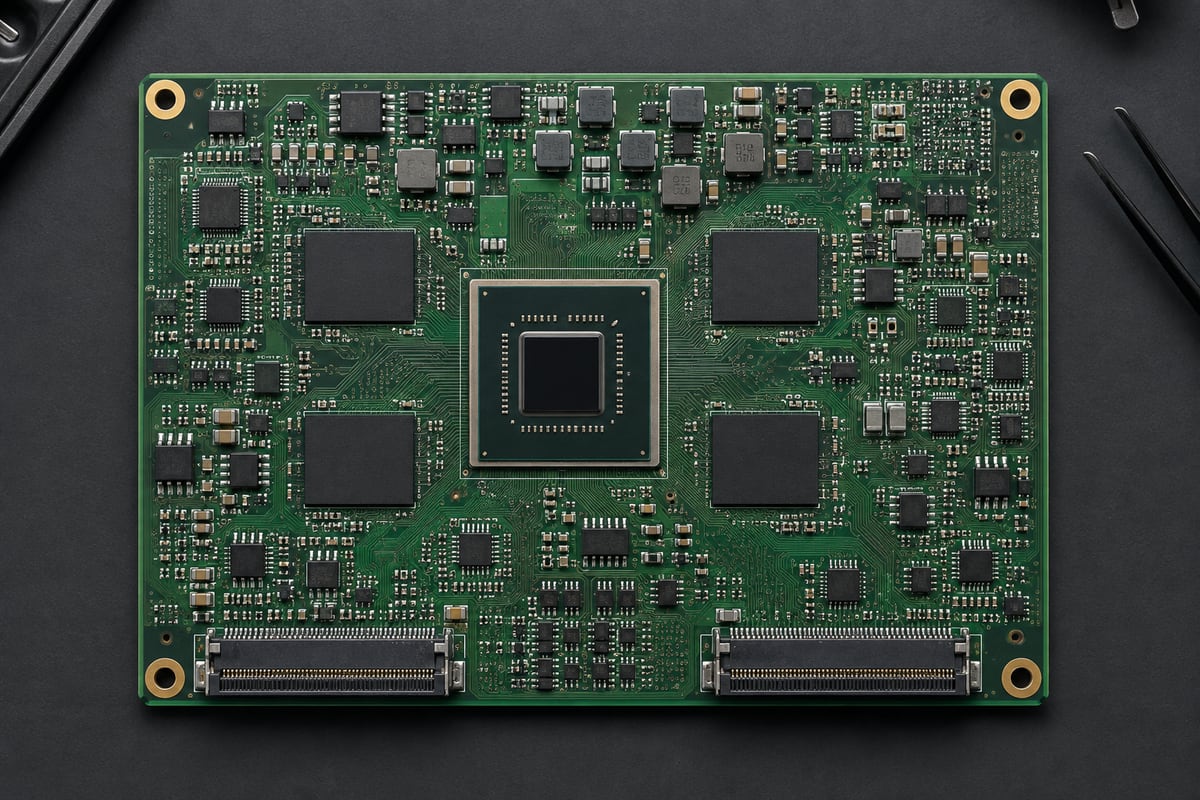
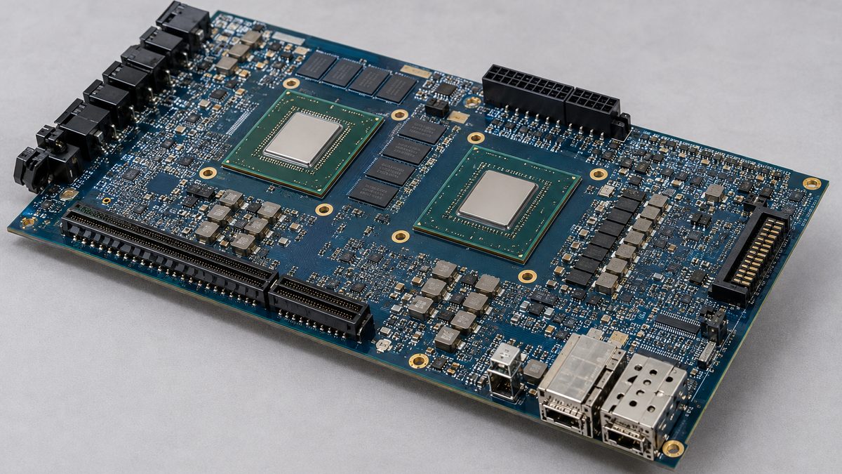
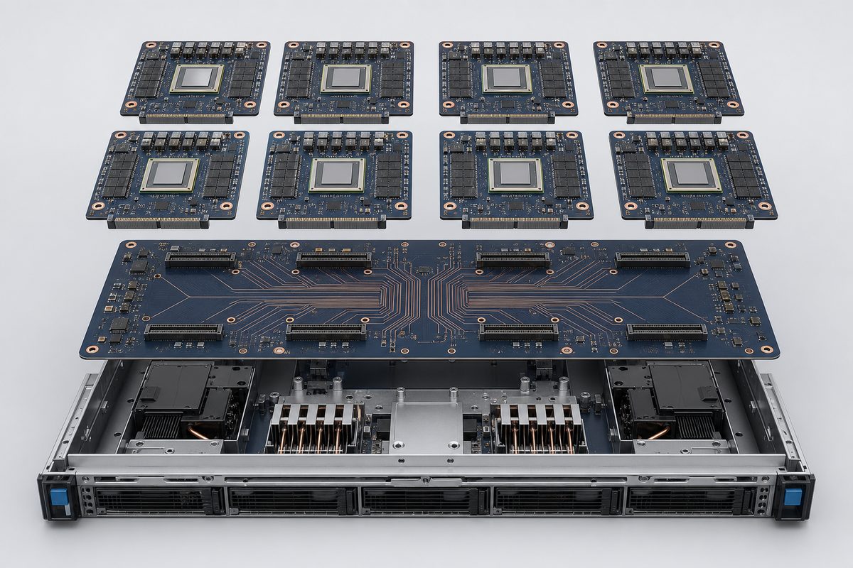
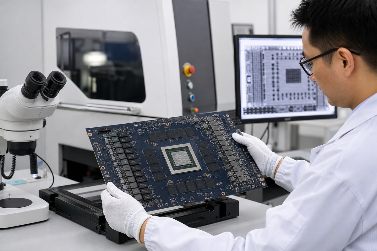
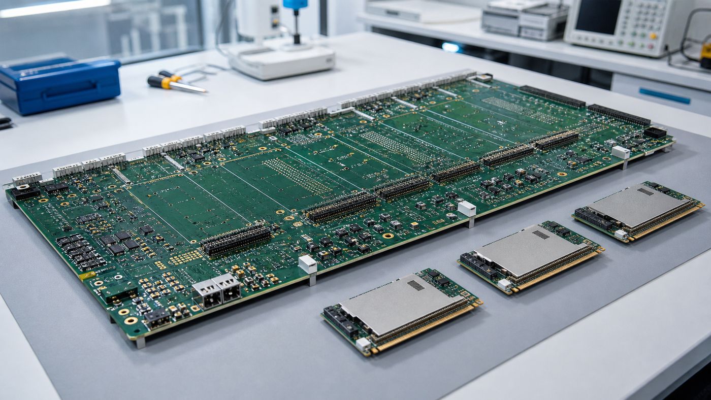
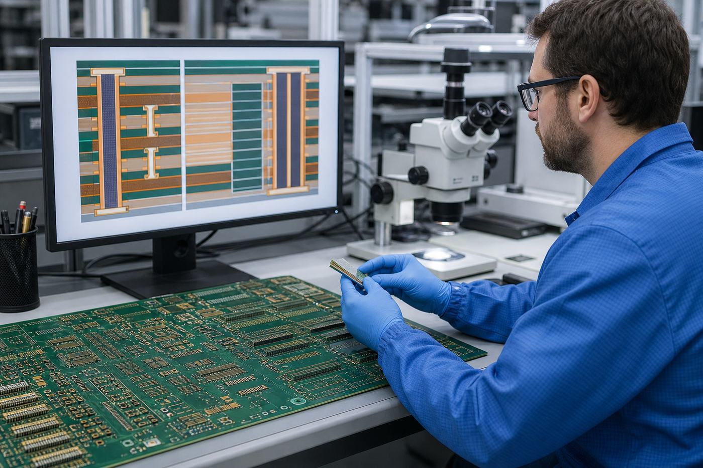
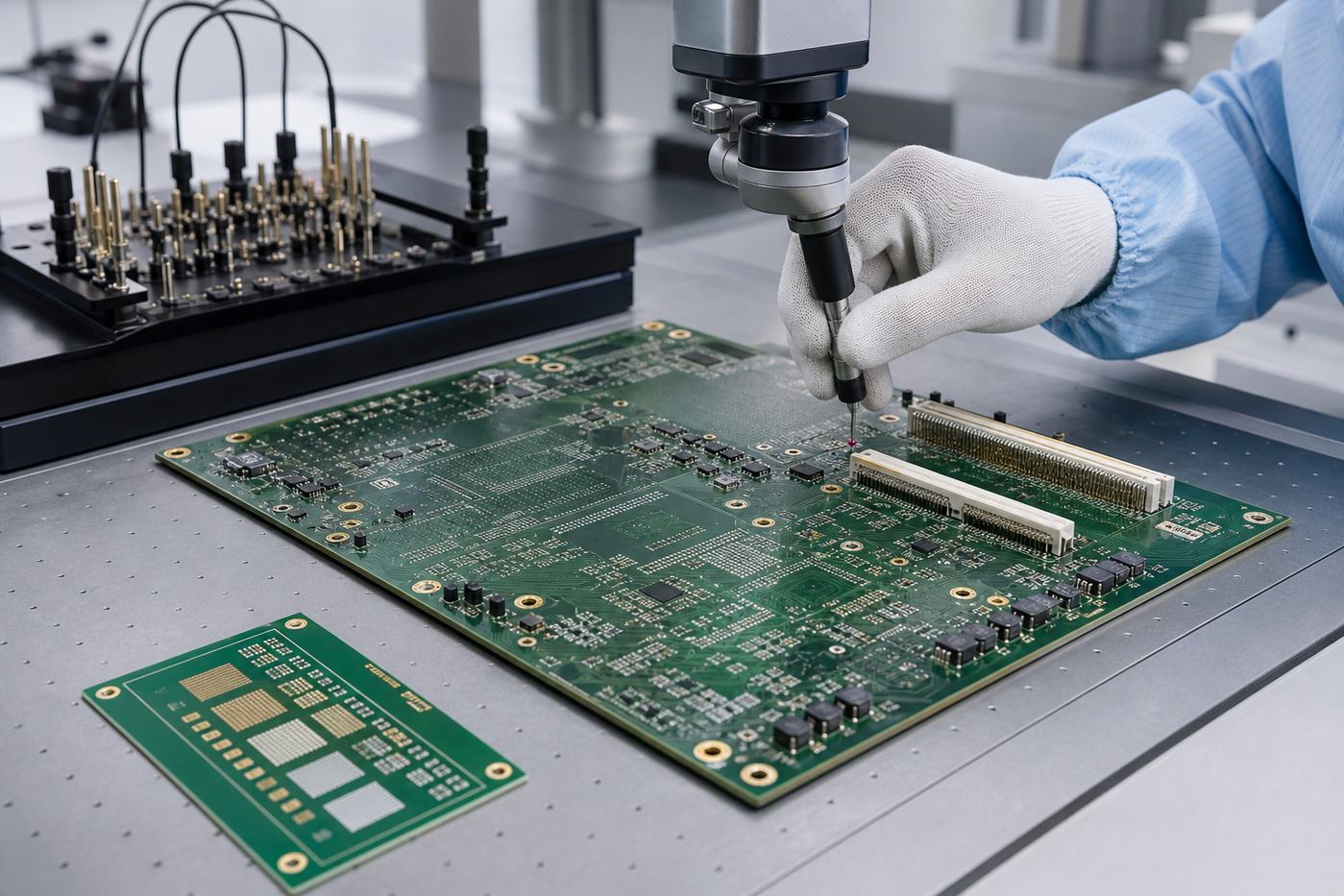
For teams searching AI hardware PCB manufacturer USA, the real challenge is not finding a company that can make a multilayer PCB. AI accelerators, edge-computing modules, machine-vision controllers, robotics platforms, and other high-performance hardware often combine fine-pitch BGAs, high-speed interfaces, controlled impedance, dense power delivery, and thermal constraints on the same board. The better supplier is the one that can support these requirements from prototype through repeat production.

EBest Circuit supports U.S. AI hardware projects through PCB fabrication, PCBA, component sourcing, testing, and box build from our manufacturing operations in China and Vietnam. If you already have a design, send your Gerber or ODB++, stack-up, BOM, assembly files, impedance requirements, quantity, and test requirements to sales@bestpcbs.com for an engineering review.

AI hardware PCB manufacturer USA

What Does an AI Hardware PCB Manufacturer Actually Need to Handle?

A manufacturer does not become an AI hardware PCB specialist simply by offering high-layer-count boards. The supplier needs to manage several constraints at the same time.

Typical AI hardware may include:

  • GPU, FPGA, NPU, or SoC packages
  • DDR memory
  • PCIe, Ethernet, USB, MIPI, or SerDes interfaces
  • Fine-pitch BGA escape routing
  • Multiple power rails
  • High-current processor supplies
  • Controlled-impedance traces
  • Dense passive components
  • Thermal vias or copper reinforcement
  • Tight SMT and inspection requirements

These requirements interact with one another.

Changing dielectric thickness can affect impedance. Increasing copper weight can alter the stack-up and etching process. A via change around a BGA may make routing easier but increase fabrication difficulty. A board can therefore be electrically correct and still be poorly suited to production.

Can the manufacturer evaluate fabrication, assembly, high-speed constraints, thermal structures, sourcing, and testability as one manufacturing problem?

That is a better indicator of whether the supplier is ready for a real AI hardware project.

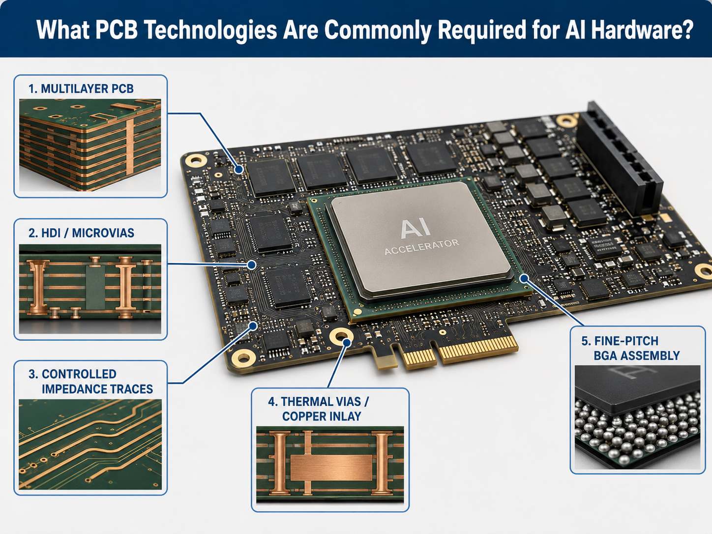
What PCB Technologies Are Commonly Required for AI Hardware?

Not every AI board needs HDI, Rogers material, or heavy copper. PCB technology should follow the actual electrical, thermal, routing, and mechanical requirements.

AI hardware PCB manufacturer USA
AI Hardware Need Common PCB Solution
GPU / FPGA / NPU Multilayer PCB
PCIe / SerDes / Ethernet Controlled impedance
Fine-pitch BGA HDI / microvias
High current Thicker copper / power planes
High heat density Thermal vias / copper inlay
Compact edge AI HDI + fine-pitch SMT
RF or very high-speed section Low-loss laminate
High I/O count More routing layers

Over-specification can raise cost without improving the finished product.

If a design works reliably on a well-engineered high-Tg FR-4 stack-up, moving the entire PCB to a premium low-loss laminate may not be necessary. The same applies to HDI. It should be used where package pitch, routing density, or board size requires it.

A capable manufacturer should be able to explain where an advanced process is necessary and where the PCB can remain simpler.

What Should USA Companies Look for in an AI Hardware PCB Manufacturer?

Start with the actual board rather than a generic factory capability list.

For an AI hardware project, check four things:

  • PCB fit: layer count, HDI structure, via-in-pad, impedance, material, copper weight, and thickness.
  • Assembly fit: fine-pitch BGA, QFN/LGA, double-sided SMT, and high thermal-mass boards.
  • Inspection and test: SPI, AOI, X-ray, electrical test, ICT, programming, and functional test where required.
  • Scale-up support: BOM sourcing, revision control, traceability, test fixtures, repeat orders, and volume ramp-up.

Before placing an order, ask the supplier to confirm the critical requirements against your released Gerber, stack-up, BOM, and assembly data.

The best supplier is not the one with the longest capability list, but the one whose process window matches your board.

Top 15 AI Hardware PCB Manufacturers in the USA

The U.S. has several PCB and electronics manufacturers capable of supporting complex computing, high-speed digital, HDI, advanced assembly, and high-reliability hardware.

The list below is intended as a practical supplier-comparison starting point rather than a strict ranking. Some companies focus more heavily on bare PCB fabrication, while others provide broader PCBA or EMS services.

Manufacturer Key Strength Good Fit For
TTM Technologies Advanced multilayer, HDI Servers, accelerators
Sanmina Complex high-layer PCB High-end computing
Summit Interconnect HDI, RF, rigid-flex Advanced NPI
AdvancedPCB HDI, impedance, quick-turn Prototype to production
Sierra Circuits UHDI, prototype engineering Dense AI boards
Calumet Electronics Advanced domestic PCB High-reliability projects
American Standard Circuits UHDI, RF, thermal PCB Mixed high-speed designs
Bay Area Circuits Quick-turn high-speed PCB Engineering prototypes
RUSH PCB HDI and turnkey PCBA Fast prototype builds
Epec Broad PCB technologies Industrial electronics
MacroFab Digital PCBA manufacturing Startup scaling
Green Circuits Complex SMT and testing Edge AI / robotics
SVTronics PCB + PCBA + integration Complete hardware builds
Creation Technologies Large-scale EMS Production programs
Sierra Assembly Technology Quick-turn assembly Low-volume complex PCBA

The next step is not simply choosing the largest company in the table. Narrow the list according to the actual PCB and production model.

If the project requires U.S.-only manufacturing because of contractual, security, ITAR, or supply-chain requirements, domestic production may be mandatory.

If it does not, compare suppliers on:

  • Technical fit
  • Engineering support
  • Lead time
  • Scalability
  • Component sourcing
  • Production cost

The practical sourcing question is:

Which supplier can build this board correctly now and continue supporting it when volume increases?

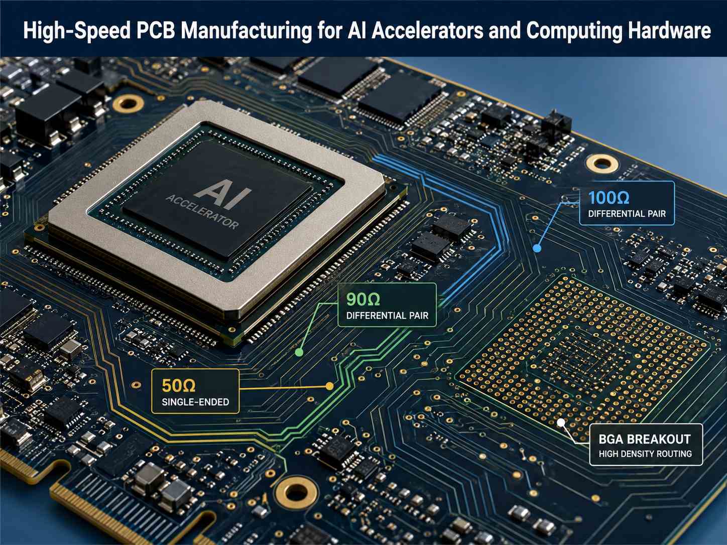
High-Speed PCB Manufacturing for AI Accelerators and Computing Hardware

High-speed interfaces are one of the main reasons AI hardware becomes difficult to manufacture.

AI hardware PCB manufacturer USA

Typical interfaces include:

  • PCIe
  • DDR
  • Ethernet
  • SerDes
  • USB
  • MIPI
  • High-speed clock networks

Common impedance targets include 50 Ω single-ended and 90 Ω or 100 Ω differential, although the customer’s released design requirement should always determine the final specification.

For a controlled-impedance RFQ, useful manufacturing data includes:

  • Target impedance
  • Signal layer
  • Reference plane
  • Trace width and spacing
  • Copper thickness
  • Dielectric thickness
  • Material grade

Material selection also matters. High-Tg FR-4 is suitable for many AI boards, while lower-loss laminates become more useful when channel-loss requirements are tighter.

At EBest Circuit, we normally ask for more than Gerber files when reviewing a high-speed board. Providing the stack-up, material grade, dielectric thickness, copper weight, and target impedance allows our engineering team to review the structure before fabrication.

How Should Power and Thermal Management Be Built into an AI PCB?

A high-performance processor can create significant electrical and thermal load in a relatively small PCB area.

The board may therefore need to support both current delivery and heat spreading.

Common options include:

  • Wide copper areas
  • Solid power and ground planes
  • Higher copper weight
  • Thermal-via arrays
  • Local copper spreading
  • Copper coin or copper inlay

The correct solution depends on the heat path.

Thermal vias are useful when heat needs to move vertically through the PCB. Copper inlay becomes more attractive when a component requires a stronger direct thermal path.

Heavy copper can also support high-current sections, but increasing copper thickness affects etching, lamination, resin fill, and line-width control. It should therefore be considered during stack-up development rather than added late in the purchasing process.

For a useful thermal review, provide the manufacturer with:

  • Copper weight
  • High-current net information
  • Major heat sources
  • Thermal-via requirements
  • Maximum board thickness
  • Heat-sink or enclosure constraints

This gives the factory enough information to identify manufacturing conflicts before production.

Why HDI and Fine-Pitch Assembly Matter in Compact AI Hardware

Edge AI devices, robotics controllers, embedded vision systems, and smart cameras often need a large amount of processing capability in a small enclosure.

That creates dense routing around BGA devices.

HDI can provide more routing freedom through:

  • Laser microvias
  • Blind and buried vias
  • Via-in-pad
  • Sequential lamination
  • Smaller capture pads

Microvias around 150 μm or below are commonly used in HDI construction, although the correct size depends on dielectric thickness, pad geometry, aspect ratio, and reliability requirements.

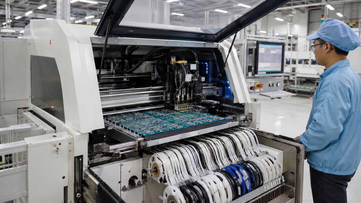
PCB fabrication is only one part of the problem. The assembly process must also control:

  • Solder paste
  • Placement accuracy
  • Reflow profile
  • BGA warpage
  • Moisture-sensitive devices
  • Hidden solder joints

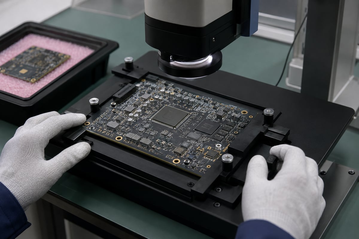
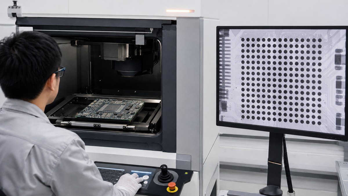
SPI is useful before placement. AOI checks visible assembly defects, while X-ray is more useful for BGA, QFN, and other bottom-terminated packages.

For dense AI hardware, having PCB fabrication and PCBA managed by the same manufacturing partner can also reduce handoff risk when a yield issue appears.

PCB Assembly and Component Sourcing for AI Hardware Projects

A complex BOM can delay an AI hardware project even when the PCB itself is ready.

Common devices include:

  • FPGA, NPU, MCU, or SoC
  • DDR and Flash memory
  • PMIC
  • Ethernet PHY
  • MOSFETs
  • Clock ICs
  • Sensors
  • High-speed connectors

Before production, the BOM should be checked for:

  • Manufacturer part number
  • Lifecycle status
  • Stock availability
  • MOQ
  • Approved alternatives
  • MSL level
  • Programming requirements

Traceability is also important for expensive processors, memory devices, and programmable components.

One practical model for early production is PCB kitting with mixed sourcing. A customer may consign the key FPGA, processor, or memory devices while allowing the PCBA supplier to source standard resistors, capacitors, power components, and connectors.

EBest Circuit supports turnkey, partial-turnkey, and customer-consigned assembly, so the sourcing model can change as the project moves from prototype into production.

How Can DFM Reduce AI Hardware Prototype Risk?

DFM should reduce the chance of discovering expensive manufacturing issues after the boards are already built.

For an AI hardware PCB, useful DFM checks include:

  • Trace and spacing
  • Annular ring
  • Hole-to-copper clearance
  • BGA breakout
  • Microvia structure
  • Via-in-pad
  • Copper balance
  • Stack-up
  • Controlled impedance
  • Solder-mask openings
  • Component clearance
  • Panelization

The important distinction is that manufacturable does not always mean production-ready.

A BGA breakout may technically be buildable but unnecessarily expensive. A stack-up may work for a prototype while leaving very little process margin for repeat production. A component placement may look acceptable in CAD but create inspection or rework problems after assembly.

At EBest Circuit, our DFM review looks at the PCB and PCBA together rather than treating fabrication as a separate step. For AI hardware projects, we review the stack-up, via structure, BGA escape routing, impedance requirements, copper distribution, solder-mask design, assembly clearance, and panelization before production. When HDI, fine-pitch BGA, heavy copper, or low-loss materials are involved, we also check whether the selected process is practical for both prototype and later production.

The better target is a PCB that can be fabricated, assembled, inspected, tested, and repeated consistently as volume increases.

USA AI Hardware PCB Case Study: From Prototype DFM to Stable Production

A U.S. customer required a 6-layer PCB for an AI accelerator. The board used FR-4 Tg 180°C with a finished thickness of 1.0 ± 0.1 mm, while the manufacturing requirements included 50 Ω impedance, resin-filled vias, Class 3 hole copper, serialization, and board-warpage control.

Project Specifications

Item Requirement
Layer count 6 layers
Material FR-4, Tg 180°C
Thickness 1.0 ± 0.1 mm
Copper 1 oz each layer
Impedance 50 Ω
Via treatment Resin-filled and plated flat
Hole copper ≥20 μm
Surface finish ENIG, 5 μin Au
Serialization LP-01# to LP-20#

Challenge

The thin 6-layer construction required careful stack-up, copper balance, and panel control to reduce bow and twist while maintaining 50 Ω impedance. All vias also required resin filling and plating, and only the individual serial numbers could remain on the silkscreen.

EBest Circuit Solution

Before production, we reviewed the stack-up, impedance structure, via process, panelization, and marking requirements together. Production data was then sent to the customer for approval before fabrication.

Result

The project established a controlled manufacturing setup for repeat builds, with the key impedance, via, hole-copper, serialization, and flatness requirements defined before production release.

For AI hardware PCB prototypes, stable production starts with controlling the manufacturing details before the first build.

AI hardware PCB manufacturer USA

What Testing Should Be Used for AI Hardware PCB and PCBA?

Testing should follow the manufacturing stage and the actual failure risk.

Stage Typical Check
Bare PCB Electrical test
Impedance PCB Impedance test
Paste printing SPI
SMT AOI
BGA / QFN X-ray
Finished PCBA ICT / functional test

Functional testing should be tied to the product rather than reduced to a simple power-on check.

Depending on the hardware, a test procedure may verify:

  • Power rails
  • Current consumption
  • Boot status
  • Firmware programming
  • Ethernet
  • USB
  • Sensors
  • Display output
  • Fan control

If the customer already has a fixture or test procedure, it should be included in the RFQ package. If not, the test method should be discussed before volume production begins.

Prototype or Mass Production: Which Manufacturing Model Fits Your AI Hardware Project?

AI hardware manufacturing changes as the product moves through development.

Prototype

The priorities are speed, engineering feedback, and design learning.

At this stage:

  • Quantities are small
  • Revisions are frequent
  • The BOM may still change
  • DFM feedback often matters more than final unit cost

EVT / DVT / PVT

The manufacturing process should begin to stabilize:

  • Stack-up
  • Material
  • BOM
  • Assembly process
  • Test fixture
  • Programming
  • Work instructions

This is where many issues that were acceptable on five boards become expensive.

Volume production

The focus shifts toward:

  • Yield
  • Repeatability
  • Traceability
  • Component continuity
  • Test coverage
  • Cost
  • Capacity

If the product is expected to scale, supplier selection should consider the next manufacturing stage as well as the current one.

Changing PCB or PCBA suppliers immediately after prototype validation can add another engineering qualification cycle and slow production ramp-up.

Why USA AI Hardware Companies Work With EBest Circuit

If your project requires U.S.-only manufacturing, EBest Circuit may not be the right fit because our manufacturing operations are based in China and Vietnam.

For U.S. companies open to global manufacturing, we offer one manufacturing partner for complex PCB fabrication, component sourcing, assembly, testing, and production scaling.

Our capabilities relevant to AI hardware include:

  • High-layer-count and HDI PCB
  • Controlled-impedance and high-speed PCB
  • Rogers and hybrid constructions
  • Heavy copper and copper inlay
  • Fine-pitch BGA assembly
  • SPI, AOI, X-ray, ICT, and functional testing
  • Turnkey component sourcing and programming
  • Prototype through volume production

For an AI accelerator, edge AI device, machine-vision controller, or other high-density computing board, we prefer to review the actual design rather than qualify the project from a generic capability list.

Send us the Gerber or ODB++, stack-up, BOM, impedance requirements, assembly files, and test requirements. Our engineering team can check whether the PCB construction, BGA routing approach, materials, copper requirements, assembly process, and test plan fit the intended manufacturing process before production.

Our quality systems cover ISO 9001, ISO 13485, IATF 16949, and AS9100D requirements, supporting projects that require controlled and traceable manufacturing processes.

What Should You Send for an AI Hardware PCB Quote?

A complete RFQ makes the engineering review faster and reduces assumptions in the quotation.

For PCB fabrication, send:

  • Gerber or ODB++
  • Fabrication drawing
  • Stack-up
  • Material requirement
  • Copper weight
  • Surface finish
  • Via specification
  • Impedance requirements
  • Quantity

For PCBA, add:

  • BOM
  • Pick-and-place file
  • Assembly drawing
  • Programming files
  • Test requirements

For high-speed boards, also include the target impedance, material grade, dielectric thickness, copper weight, and relevant interface information.

If the design is still in development, you do not need to wait until every production document is complete. The latest Gerber, BOM, stack-up, quantity, and key requirements are usually enough for an initial manufacturing review.

FAQs About AI Hardware PCB Manufacturing

1. What type of PCB is used in AI hardware?

AI hardware commonly uses multilayer rigid PCB, HDI PCB, rigid-flex PCB, or a combination of high-speed and high-current PCB technologies. The correct construction depends on processor package, routing density, interface speed, current, and thermal requirements.

2. Can AI hardware PCBs use standard FR-4?

Yes. Many AI boards can use high-Tg FR-4. A low-loss laminate is normally justified when high-speed channel loss, impedance stability, or frequency requirements exceed what the selected FR-4 system can comfortably support.

3. Do AI accelerator boards require HDI?

Not always. HDI is most useful when fine-pitch BGAs, high I/O density, limited board area, or difficult escape routing make conventional through-via construction inefficient.

4. What materials are suitable for high-speed AI PCBs?

High-Tg FR-4 works for many applications. Low-loss laminates, Rogers materials, or hybrid stack-ups can be considered when signal-loss requirements are more demanding.

5. Can EBest Circuit manufacture AI hardware PCBs for USA customers?

Yes. We support U.S. customers through our China and Vietnam manufacturing operations, covering PCB fabrication, component sourcing, PCBA, inspection, testing, programming, and box build.

6. What files are required for an AI hardware PCB quotation?

For PCB fabrication, send Gerber or ODB++, stack-up, specifications, material, copper weight, impedance targets, quantity, and finish requirements. For PCBA, also provide the BOM, pick-and-place file, assembly drawing, programming files, and test requirements.

Ready to Discuss Your AI Hardware PCB Project?

If you are developing an AI accelerator, edge AI device, machine-vision system, robotics controller, AI computing module, or other high-performance hardware, send your Gerber or ODB++, stack-up, BOM, assembly files, impedance requirements, quantity, and test requirements to sales@bestpcbs.com. Our engineering team can review the project before quotation and help identify PCB fabrication, assembly, sourcing, or testing issues that may affect prototype or volume production.
If you would like to evaluate our manufacturing capabilities in person, you are welcome to visit our factory. We can arrange a factory tour for your engineering or sourcing team to review our PCB fabrication, SMT assembly, inspection, testing, and quality-control processes. To evaluate EBest Circuit for your AI hardware PCB manufacturer USA project, send project files or arrange a factory visit through sales@bestpcbs.com.

You may also like

AI Hardware PCB Manufacturer for Israel Projects

September 4th, 2026

AI hardware PCB manufacturer Israel projects require more than a factory that can reproduce Gerber files. AI accelerator boards, edge-computing controllers, machine-vision systems and robotics hardware can combine dense packages, high-speed interfaces, concentrated power and demanding thermal conditions on one PCB.

Israel buyers therefore need a manufacturing partner that can review the released stackup, build controlled-impedance and HDI structures, source the approved BOM, assemble fine-pitch components and deliver inspection records with the finished boards. EBest Circuit supports these projects from China, covering PCB fabrication, component sourcing, assembly and testing without presenting itself as an Israel-based factory.

AI hardware PCB manufacturer Israel

AI Hardware PCB Manufacturers Israel Buyers Can Compare

Israel buyers can compare PCB manufacturers in Israel for close engineering communication and overseas suppliers for broader production capacity or cost control. The right shortlist depends on whether the order requires bare PCB fabrication, PCBA, system integration or all three.

Manufacturer Location Relevant services
PCB Technologies Israel Complex PCBs, PCBA and electromechanical assembly
Nistec Israel PCB assembly, NPI, procurement, testing and system integration
Sanmina Israel Israel PCBA, testing, machining, enclosures and system integration
A.L. Electronics Israel NPI, component sourcing, PCB assembly and testing
Kimron Technologies Israel Turnkey PCB assembly from prototype to production

PCB Technologies is suitable for buyers comparing locally manufactured complex PCBs, assembly and electromechanical integration.

Nistec combines local PCB assembly, procurement, testing and product integration. Its group also includes Eltek for complex rigid and rigid-flex PCB fabrication.

Sanmina Israel supports complex electronics and system-level manufacturing where PCBA must be combined with mechanical parts, enclosures and final integration.

A.L. Electronics provides production engineering, sourcing, NPI, assembly, inspection and functional testing for high-mix projects.

Kimron Technologies supports turnkey electronic production in Israel, including purchasing, PCB assembly and product manufacturing.

This list is a starting point, not a ranking. Buyers should send the same controlled RFQ package to each candidate and compare technology fit, BOM responsibility, test scope, lead time, commercial terms and production location.

Israel PCB Manufacturer vs China PCBA Partner for AI Hardware

A local Israel manufacturer and a China PCBA partner can serve different stages of the same AI hardware program.

Buyer priority Israel manufacturer China PCBA partner
Face-to-face engineering Easier Remote
Local logistics Shorter International shipping
PCB technology range Supplier-dependent Broad supplier base
Component sourcing Regional network Strong Asian supply chain
Small local builds Often suitable Suitable after setup review
Scaling production Capacity-dependent Stronger cost leverage
System integration Available from selected EMS firms Define in quotation

Local production may suit an early build that requires frequent physical collaboration, rapid access to the engineering team or Israel-specific supply-chain control.

A China partner may be more competitive when the project needs HDI, high-layer-count boards, high-frequency materials, complex component sourcing or a transition from prototypes to repeat production.

EBest Circuit provides PCB fabrication and PCBA in China for Israel customers. The practical comparison should use the complete landed result: finished boards, approved components, inspection, testing, packaging, freight and the engineering time required to coordinate the order.

HDI and High-Speed PCB Capability for Israel AI Hardware Projects

AI hardware boards often place processors, memory, power devices and high-speed connectors within a limited area. Buyers need a PCB structure that can escape dense packages while preserving the signal and power conditions defined by the design team.

EBest Circuit can review released projects that require:

  • HDI and sequential-lamination structures
  • Laser-drilled microvias
  • Blind and buried vias
  • Via-in-pad and filled-via structures
  • Multilayer high-speed PCBs
  • Controlled single-ended and differential impedance
  • High-Tg, mid-loss or low-loss laminate
  • Rigid-flex construction
  • Backdrilling when specified
  • Heavy copper for high-current sections

The manufacturing package should identify the approved stackup, laminate, finished copper, impedance structures, via sequence and relevant tolerances. If a high-speed interface depends on a particular material or copper profile, substitutions should require customer approval.

A manufacturable result is the customer benefit: the released channel geometry remains tied to one confirmed stackup instead of being reinterpreted after the order enters production.

AI hardware PCB manufacturer Israel

Thermal Management for Israel AI Hardware PCB Projects

An AI processor or accelerator can create a concentrated thermal load around the package, voltage regulators and power-delivery network. The PCB manufacturer must preserve the thermal structures already defined in the released design.

Depending on the board, production may include:

  • Heavy copper power and ground areas
  • Thermal via arrays beneath hot components
  • Copper-filled or resin-filled vias
  • Metal-core or copper-base constructions
  • Copper coins or other specified heat-spreading structures
  • Controlled dielectric thickness
  • Balanced copper distribution
  • Flatness controls for heat-sink contact
  • Mechanical support around large packages

For example, a processor area that transfers heat through a via array depends on finished hole geometry, plating and the surrounding copper structure. Incomplete fill, unsuitable via dimensions or board distortion can reduce contact with the thermal interface and heat sink.

Before fabrication, buyers should release the required copper weight, via structure, board thickness, flatness criteria and mechanical drawing together. The PCB factory can then check whether the thermal construction can be produced consistently without changing the customer’s electrical or mechanical intent.

AI Server PCB Assembly for Israel Buyers

For an Israel buyer, the value of AI server PCB assembly is receiving boards that are ready for validation, rather than coordinating the bare PCB, parts and assembly through separate suppliers.

EBest Circuit supports SMT, through-hole and mixed assembly. A typical AI hardware build may include BGAs, QFNs, fine-pitch ICs, high-speed connectors, memory devices, power modules and large thermal-pad components.

The assembly workflow can include:

  1. BOM, centroid and drawing reconciliation.
  2. Component identity and quantity checks.
  3. Moisture-sensitive component control.
  4. Solder-paste inspection.
  5. Automated component placement.
  6. Controlled reflow soldering.
  7. AOI for visible joints and placement.
  8. X-ray inspection for hidden BGA or QFN joints.
  9. Through-hole and special assembly.
  10. Programming or functional testing when procedures and fixtures are supplied.

First-article inspection should be completed before the remaining units proceed. This gives the buyer an opportunity to confirm component orientation, workmanship, connector fit and agreed test results before the entire batch is assembled.

AI hardware PCB manufacturer Israel

Component Sourcing for Israel AI Hardware Production

AI hardware production can be delayed by processors, memory, connectors, power devices and other allocated or long-lead components. Buyers need a sourcing process that protects the approved BOM while keeping engineering decisions under their control.

EBest Circuit can work with turnkey, consigned or partial-turnkey material models.

Supply model Buyer provides EBest Circuit provides
Turnkey Approved BOM PCB, components and assembly
Consigned Components PCB and assembly
Partial turnkey Selected critical parts Remaining parts, PCB and assembly

For repeat production, the useful controls include:

  • Manufacturer part numbers recorded in the BOM
  • Approved distributors and supply sources
  • Lot and date-code requirements
  • Moisture and packaging checks
  • Shortage reporting before assembly
  • Customer approval before substitution
  • Remaining-component inventory records
  • BOM revision control between orders

When a specified part becomes unavailable, we can present an available alternative with supporting data for review. The substitution is implemented only after approval when it affects form, fit, function, firmware, compliance or validation.

This keeps purchasing decisions out of the design team’s daily reorder work without allowing the manufacturer to make uncontrolled component changes. PCB kitting can also expose missing, mismatched or unsuitable parts before the SMT schedule begins.

AI hardware PCB manufacturer Israel

AI Hardware PCB Lead Time for Israel Buyers

Lead time begins after the files, commercial terms and engineering questions are confirmed. A short assembly time does not help if the PCB stackup remains unresolved or a critical processor is unavailable.

EBest Circuit’s reference production times are:

Production scope Reference lead time
1-layer FR-4 prototype 3–4 days
2-layer FR-4 prototype 4–6 days
4–6 layer FR-4 prototype 8–10 days
8-layer FR-4 prototype 10–14 days
10-layer FR-4 prototype 14–18 days
HDI PCB About 2.5–3.5 weeks
PCBA after materials are ready About 1 week

Express options may be available for suitable projects. Complex HDI cycles, special laminate procurement, long-lead components, functional-test development and approval delays can extend the schedule.

Israel buyers should request four dates separately:

  • Engineering release
  • Bare PCB completion
  • PCBA completion
  • Arrival in Israel

This makes the delivery commitment easier to evaluate because international transport is not hidden inside an undefined production estimate.

Quality Control for Israel AI Hardware PCB Orders

Quality control should give the buyer evidence that the correct revision, materials, components and tests were used. It should not be limited to a final visual inspection.

For bare PCBs, the agreed controls may include:

  • Incoming laminate verification
  • Inner-layer AOI
  • Layer registration checks
  • Drilling and plating control
  • Electrical testing
  • Controlled-impedance testing
  • Microsection analysis
  • Finished dimensions
  • Surface-finish inspection
  • Bow and twist measurement

For PCBA, inspection may include SPI, first-article inspection, AOI, X-ray, visual inspection and functional testing. The actual test scope should be agreed before quotation because AOI and X-ray cannot prove firmware operation or complete product performance.

EBest Circuit’s quality qualifications include ISO 9001:2015, ISO 13485:2016, IATF 16949 and AS9100D. Buyers should confirm which certification, workmanship standard, records and acceptance criteria apply to their specific project.

MES-based production records can connect materials, process stages and inspection results to the order. For repeat builds, that traceability helps the buyer determine whether a failure is linked to a component lot, manufacturing stage, approved deviation or design revision.

AI hardware PCB manufacturer Israel

AI Hardware PCB Case Study for an Israel Project

An Israel AI hardware customer needed a compact assembled board containing a dense processor area, high-speed interfaces and several power rails. The order required bare PCB fabrication, component sourcing, SMT assembly and inspection.

Project requirement: The customer wanted a small prototype batch for hardware and firmware validation before releasing the next production quantity.

Manufacturing risk: The fabrication data, impedance table and assembly package had to describe the same board revision. A mismatch would have delayed assembly or produced boards that could not be compared reliably during validation.

Action: Before production, the PCB stackup, controlled-impedance structures, drill data, BOM, centroid file and assembly drawing were checked together. Open items were returned to the customer for confirmation before materials were released.

The PCB was manufactured after the build package had been aligned. Components were then prepared for SMT assembly, with first-article, AOI and X-ray inspection applied according to the package mix.

Result: The customer received one controlled prototype build for validation instead of separate PCB and assembly outputs based on different assumptions. The confirmed fabrication and assembly data also provided a clearer baseline for the following order.

Customer-identifying information and proprietary design details are excluded. Project-specific electrical performance remains subject to the customer’s validation procedure and final system conditions.

FAQs About AI Hardware PCB Manufacturing for Israel

Can EBest Circuit manufacture AI hardware PCBs for customers in Israel?

Yes. EBest Circuit manufactures in China and supports quotation, fabrication, component sourcing, assembly, inspection and international delivery for Israel customers.

Can you manufacture a PCB from a completed Israel engineering design?

Yes. Send the released fabrication data, drawings, stackup and assembly package. We review manufacturability but do not change the customer’s electrical design without approval.

What files are required for quotation?

Provide Gerber or ODB++ files, NC drill data, fabrication drawing, stackup, BOM, centroid file, assembly drawings, quantities and test requirements.

Can you assemble customer-supplied processors or other critical components?

Yes. Consigned parts can be reviewed for quantity, packaging, moisture condition, traceability and assembly suitability before production.

Can alternative components be used when the original part is unavailable?

An alternative can be proposed, but implementation should follow the customer’s approval process. The manufacturer should not make an uncontrolled substitution.

Can EBest Circuit build HDI boards for AI accelerator hardware?

HDI projects can be reviewed according to their layer structure, microvia sequence, material, registration limits, via filling and assembly requirements.

Do all AI hardware boards need low-loss material?

No. Material selection should follow the interface speed, channel length, insertion-loss budget, stackup and operating environment. Some control or power boards may use high-Tg FR-4.

Can you perform functional testing?

Functional testing can be included when the customer supplies an approved procedure, acceptance limits and any required fixture, software or programming files.

How should confidential project files be sent?

File access, revision control and confidentiality requirements should be agreed before transfer. Each supplier should receive only the controlled information required for its work.

How can an Israel buyer request a quote?

Send the PCB files, BOM, order quantity, delivery destination and required test scope to sales@bestpcbs.com. We will review the manufacturing package and confirm the available production route, open engineering questions and lead time for your AI hardware PCB manufacturer Israel project.
You may also like

Why Use Co-Packaged Optics in AI Data Centers?

September 2nd, 2026

Co-packaged optics places optical engines beside a processor or switch chip within a common package assembly. Moving electrical-to-optical conversion closer to the silicon shortens the high-speed connection that would otherwise cross a board to a front-panel transceiver. For AI data centers, this can provide more bandwidth within interconnect power and space limits. The exchange is tighter integration: package design, cooling, fiber handling, and service procedures become more demanding. A useful platform comparison weighs those costs against the electrical bottleneck CPO can remove.

Co-packaged optics, conceptual unbranded chip-and-optical-engine assembly with pale fiber loops and the article title

What Is Co-Packaged Optics (CPO)?

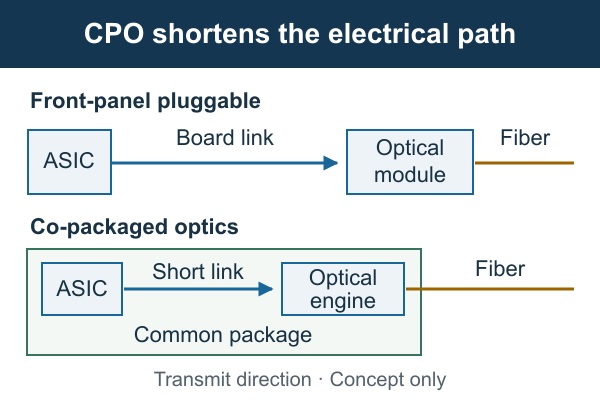
Co-packaged optics is an integration approach, not a network protocol or a particular optical speed. A switch application-specific integrated circuit (ASIC) still processes traffic electronically. Nearby optical engines convert outgoing data into optical signals and convert received light back into electrical signals.

In a conventional pluggable design, the ASIC connects electrically to a transceiver at the chassis faceplate. In CPO, the optical engine shares a package-level assembly with the ASIC; fiber carries the optical signal toward the faceplate and onward. The engines do not have to be fabricated on the same silicon die as the processor.

This distinction matters when reading product descriptions. A device can use silicon photonics inside a front-panel module without being co-packaged. Conversely, a CPO label alone does not specify the laser location, optical reach, cooling method, or replaceable unit. Those details belong to the implementation.

Why Is Co-Packaged Optics Important for AI Data Centers?

CPO addresses the electrical distance and power needed to move data between high-bandwidth chips and optical links. Distributed training exchanges gradients and other data across accelerators; some inference deployments also move substantial traffic between compute nodes. When communication delays useful computation, adding more GPUs does not necessarily produce a proportional gain.

As electrical signaling rates rise, package transitions, board traces, vias, and connectors consume channel margin. Equalization and retiming can recover degraded signals, but they require power and introduce design constraints. Moving conversion closer to the ASIC reduces the electrical path that must sustain the highest rates.

  • Interconnect power: A shorter electrical channel can reduce signal-conditioning requirements. Compare complete link power at equal delivered bandwidth, including host I/O, optical engines, lasers, and any cooling overhead; module watts alone are not a system comparison.
  • Bandwidth density: Optical engines near the chip can reduce dependence on long electrical escapes to front-panel modules. The resulting design must still accommodate fiber exits, connectors, cooling hardware, and assembly access.
  • Useful compute time: A stable, adequately provisioned fabric helps keep accelerators supplied with data. Confirm the benefit with representative communication patterns and job-completion measurements, since CPO cannot fix oversubscription, congestion policy, or an inefficient training strategy.

The strongest case is a system whose electrical I/O power, channel margin, or packaging density is already limiting its next bandwidth step. A smaller installation with adequate links and strict field-replacement requirements may have little reason to change architectures.

How Does Co-Packaged Optics Work?

The signal changes from electrical to optical close to the ASIC, then follows an optical link to its destination. The shortened segment is the local chip-to-engine connection; CPO does not turn the processor or every connection on the board into an optical device.

  1. Generate the electrical signal. The ASIC’s serializer/deserializer (SerDes) sends high-speed electrical data over a package-level connection to the optical engine. Channel validation checks whether that interface meets the selected electrical specification.
  2. Modulate the light. Driver electronics control an optical modulator using light supplied by the laser arrangement. The resulting optical waveform carries the data; the laser may be external to the hot package.
  3. Couple into fiber. Optical couplers and fiber attachments transfer light from the engine into the fiber path. Coupling loss, connector loss, and fiber loss consume the link’s optical budget.
  4. Recover the received data. A photodetector converts incoming light into current, and receiver electronics recover an electrical signal for the destination. End-to-end error measurements verify the link, including the agreed error-correction conditions.
Co-packaged optics, simplified transmit paths comparing board-level electrical routing to a pluggable module with a short package connection to an optical engine

What Are the Main Components of a CPO System?

A working CPO system needs an electrical processor, optical conversion, a light source, and mechanical and thermal support. A block diagram should identify who supplies and validates each interface, not merely name the chips.

  • Switch ASIC or compute device: Generates and receives data through compatible electrical I/O. Its lane configuration and management requirements constrain the engine arrangement.
  • Optical engine: Combines photonic functions with driver and receiver electronics. Check both electrical and optical interfaces; an advertised aggregate bandwidth does not establish compatibility.
  • Laser source: Supplies optical power. An external laser can separate laser servicing and some thermal concerns from the main package, but adds delivery fibers, connections, and its own fault-management requirements.
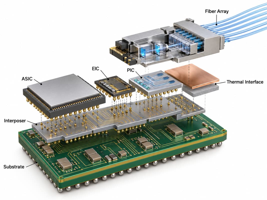
  • Package substrate and interconnect: Connect the ASIC and engines while supporting power distribution and mechanical attachment. Electrical, thermal, and assembly constraints must be reviewed together.
  • Fiber attachment and connectors: Route light between the engines and the external network. Alignment, bend limits, contamination control, and access determine whether the link remains usable after assembly and servicing.
  • Host board, cooling, and control: Provide power, monitoring, mechanical support, and heat removal. These remain necessary even when selected high-speed traces no longer traverse the host PCB.

How Do CPO, NPO, and LPO Compare with Pluggable Optics?

Compare physical integration first, then compare signal processing. Front-panel pluggable optics, near-package optics (NPO), and CPO describe where conversion sits. Linear pluggable optics (LPO) is a type of pluggable optical implementation, not a fourth mutually exclusive location.

Physical placement determines which electrical path must be designed.
Integration Conversion location Design consequence
Front-panel pluggable Removable module at the faceplate The host electrical channel reaches the module; module replacement is accessible.
Near-package optics Close to, but outside, the ASIC’s package A shorter board-level path is possible; mounting and service access depend on the design.
Co-packaged optics Optical engines in a common package assembly with the ASIC The critical electrical connection moves into the package; optical and cooling integration become central.

Within the pluggable category, a conventional retimed module includes digital signal processing, while LPO removes the module DSP and relies on suitable host SerDes capabilities across the link. The LPO MSA’s interface explanation makes that distinction explicit. LPO therefore preserves a pluggable form factor while changing host-channel and interoperability requirements.

A useful evaluation asks two separate questions: where should conversion occur, and where should equalization or retiming occur? CPO is not automatically the lowest-power or lowest-cost answer, and LPO is not a drop-in upgrade for every existing port. Compare validated configurations at the same reach, bandwidth, error performance, and maintenance requirements.

How Is CPO Used in Scale-Up and Scale-Out AI Networks?

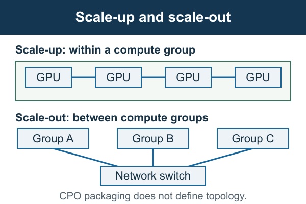
CPO can support either network domain, but scale-up and scale-out describe communication roles rather than packaging choices. The correct starting point is the required topology, protocol, distance, and latency—not the assumption that every AI link needs optics.

Scale-up connects accelerators into a tightly coupled compute system. Such links can have demanding latency, bandwidth, and memory-access requirements. Copper remains useful for suitable short connections; optical I/O becomes relevant when the required reach or system size exceeds the practical electrical design.

Scale-out connects servers or compute groups through a wider network fabric. A CPO switch can place conversion near its switching ASIC while a server endpoint still uses a compatible pluggable transceiver. The endpoints need matching optical interfaces and protocol behavior, not matching packaging labels.

Co-packaged optics, conceptual scale-up accelerator links and scale-out compute groups connected through a network switch, without a vendor-specific topology

Before a comparison, list the traffic that crosses each boundary: accelerator-to-accelerator exchanges, server-to-server collectives, and traffic between larger clusters. Then identify where electrical reach or power becomes restrictive. This avoids spending a packaging premium on links that are not the bottleneck.

What Does CPO Change for PCB and Package Design?

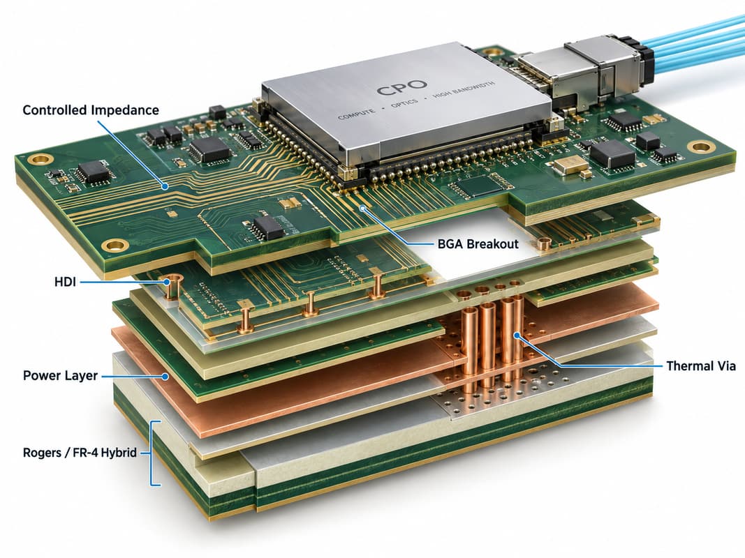
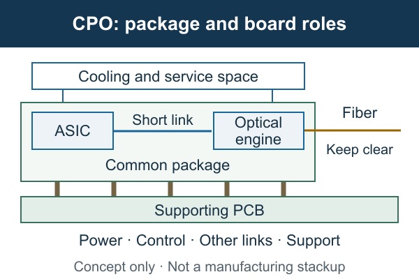
CPO moves selected high-speed design problems into the package; it does not remove the need for a carefully engineered PCB. The package team owns the chip-to-engine connection. The board team still has to deliver power, route remaining interfaces, support the assembly, and provide usable access for cooling and fiber handling.

Co-packaged optics, conceptual package and supporting PCB responsibilities for fiber, cooling, power and control; not a manufacturing stackup

Package and board channels. A chip-to-engine connection confined to the package should not be assigned a host-PCB trace budget. Remaining high-speed board interfaces still require loss, reflection, crosstalk, and return-path analysis. Build a channel map showing every transmitter, receiver, transition, and connector before selecting materials.

This is why “CPO allows a cheaper PCB” is an incomplete conclusion. Fewer long optical-module routes may ease one constraint, while dense package escape, power delivery, other high-speed links, and assembly requirements continue to influence the stackup. Select laminate and via construction from the remaining channel budgets and fabrication tolerances, not from the CPO label.

Power delivery. ASIC load changes can create rail droop or noise if the board-package power-delivery network (PDN) has excessive impedance. Optical electronics may have separate supply-noise limits. Obtain rail specifications, transient-load information, package models, and decoupling constraints; then evaluate the combined PDN rather than checking the board in isolation.

The useful output is a set of verified rail margins over the relevant operating conditions. Where measurements disagree with simulation, investigate the model boundary, probe setup, and current transient before adding capacitors indiscriminately. Coordinate these checks with the stackup and channel budgets used in AI server PCB design.

Cooling, warpage, and fiber access. Optical engines near a hot ASIC must remain within their specified thermal conditions. Heat-sink or cold-plate hardware needs clearance, mounting loads, and service access. Review the full temperature distribution and tolerance stack; a passing ASIC junction temperature alone does not validate neighboring optics.

Package and board deformation can affect attachment reliability and alignment-sensitive interfaces. Mechanical analysis should use the actual materials, assembly sequence, and mounting conditions. Fiber exits need protected routes with supplier-specified bend limits and strain relief, including the space a technician needs to remove adjacent hardware.

Translate each design change into a concrete engineering handoff.
Design area CPO-related change Required handoff
High-speed channel Selected paths move from host board to package. Separate package and PCB channel budgets, models, and compliance results.
Power delivery ASIC and optical supplies share a constrained assembly. Rail limits, transient models, decoupling allocation, and measured margins.
Mechanical integration Cooling hardware and fiber routes compete for access. Tolerance analysis, keep-outs, mounting loads, and service clearances.
Assembly and test An electrical board test cannot validate the complete optical path. Process sequence, optical test access, acceptance limits, and failure ownership.

Assembly and test. Agree on incoming package checks, board assembly inspection, electrical bring-up, and end-to-end optical tests before releasing fabrication data. Confirm which parts tolerate each assembly or cleaning step and when fibers are attached. Do not assume that a normal board rework process is acceptable for an integrated optical assembly.

Consider a hypothetical link that fails only after the cooling assembly is installed. Compare optical loss, rail behavior, temperature, and connector seating before assigning the fault to PCB impedance. A repeatable change in coupling loss with mechanical loading points toward the attachment or fiber path; rail disturbance under load calls for power-delivery checks. Use the observations to choose the next test instead of changing board materials first.

What Are the Main Challenges of Co-Packaged Optics?

The main challenges are achieving acceptable integrated yield, thermal behavior, test coverage, and repairability. Shortening an electrical link removes some difficulties while combining components that previously could be tested or replaced separately.

  • Yield and failure isolation: An integrated assembly can contain valuable known-good components before a later fault is found. Establish pre-assembly screening, test access, and allowed rework stages so one failed element does not automatically consume the entire assembly.
  • Temperature-dependent optical behavior: Heating can change device behavior and alignment conditions. Validate the link across specified temperatures and realistic neighboring ASIC loads, including any tuning or control overhead.
  • Fiber handling and cleanliness: Tight routing, strained attachments, or contaminated interfaces can reduce optical margin. Check loss after final mechanical assembly and after the intended maintenance procedure, not only on an open bench.
  • Serviceability: A replaceable external laser does not make an optical engine or ASIC package field-replaceable. Identify the actual failed-unit replacement procedure, the affected ports, spare requirements, and recovery time.
  • Interoperability and supply continuity: Standards alignment does not prove that arbitrary engines, hosts, and firmware work together. Require a qualified configuration and a controlled substitution process for components that affect the link.

These risks belong in a system qualification plan. Neither a low engine-power figure nor a successful demonstration answers how the platform behaves under faults, maintenance, and sustained workload.

How Mature Is CPO for Commercial Deployment?

CPO has moved beyond laboratory-only demonstrations, but procurement readiness remains product-specific. Distinguish a technology demonstration, early-access shipment, volume-production announcement, and a supported system that your organization can order and qualify.

Broadcom’s October 2025 Tomahawk 6–Davisson announcement describes a 102.4-Tb/s CPO switch and says shipments have begun. Its availability section also describes sampling to early-access customers. Before ordering, confirm whether your chosen system is in sampling, qualification, or general availability.

In its June 1, 2026 COMPUTEX update, NVIDIA states that Spectrum-X Ethernet Photonics is in full production. This is a vendor production statement, not an independent measurement of installed market share or proof that every customer’s delivery, qualification, and service requirements are satisfied.

For a purchase decision, ask the system supplier for the exact orderable configuration, qualification coverage, committed lead time, supported optics at the far end, and field-service procedure. A roadmap is useful for planning; those records are needed for deployment.

Is Co-Packaged Optics Right for Your AI Data Center?

CPO is a good fit when it delivers measurable workload gains and your team can support its integration and maintenance requirements. Compare complete network configurations at the same port rate, reach, cooling conditions, and error-correction settings. Use the following checks to test the case for deployment.

  1. Locate the bottleneck. Measure traffic demand, congestion, accelerator waiting time, and link utilization. The result should show whether network capacity, electrical I/O, or another resource constrains the job.
  2. Normalize performance and power. Compare equal usable bandwidth and reach at representative load. Record which I/O, laser, control, and cooling contributions are included.
  3. Qualify the complete link. Test the proposed host, firmware, engine, fiber, connectors, and remote endpoint together. Retain error-rate, optical-margin, and restart results under agreed conditions.
  4. Exercise maintenance and faults. Demonstrate isolation and replacement for the likely failure units. Record ports affected, recovery behavior, and the time needed to return to service.
  5. Review manufacturing and lifecycle support. Confirm production test coverage, acceptable substitutions, spares, and repair terms. Use those inputs with acquisition and operating costs to compare lifecycle expense.

A pilot should have explicit acceptance thresholds and a fallback. If the expected gain appears only in a component specification and not in the workload or operating plan, the deployment case is not yet established.

FAQs About Co-Packaged Optics

Q1. Is silicon photonics the same as co-packaged optics?

A1. No. Silicon photonics describes an implementation technology for optical functions. CPO describes their integration near an electronic chip within a package assembly. Silicon-photonics devices can also be used inside pluggable modules, so the technology name alone does not identify the packaging architecture.

Q2. Will CPO replace all pluggable transceivers?

A2. No universal replacement follows from CPO adoption. Pluggables can remain appropriate where modular replacement, varied reaches, and existing platform compatibility matter. A CPO switch can also connect to a compatible pluggable endpoint. The decision is made for a specific link and service model.

Q3. Does CPO eliminate DSPs and retimers?

A3. Not by definition. A shorter channel can change the amount and location of signal conditioning, but the CPO label does not specify every electronic function. Check the actual host and engine architecture before assuming a DSP-free path or assigning a latency saving.

Q4. Is CPO only for Ethernet switches?

A4. No. Optical integration can be applied to other switching and compute devices. Protocol support, electrical interfaces, and software integration still need to be demonstrated for the intended platform. A working Ethernet switch implementation is not proof of compatibility with an accelerator’s scale-up interface.

Q5. Does every CPO design require an external laser?

A5. No. Laser placement is an implementation choice. An external source can offer thermal separation and a replaceable laser unit, while adding optical delivery and management requirements. Confirm the specified laser arrangement and which failure units are actually replaceable.

Q6. Is there a fixed maximum reach for CPO?

A6. No. Reach depends on the optical interface, wavelength arrangement, fiber, connector losses, receiver performance, and link budget. CPO identifies where conversion takes place. Use the selected interface specification and the complete installed path to establish reach and margin.

Q7. Can CPO connect directly to an LPO endpoint?

A7. Some implementations support that configuration, but the labels alone do not guarantee it. Require a supplier-qualified combination of host, module, optical interface, firmware, and error-correction settings. Equal nominal port speeds are insufficient evidence of interoperability.

Q8. Does CPO require liquid cooling?

A8. CPO does not define a cooling method. Cooling depends on ASIC power, engine limits, package geometry, airflow or coolant conditions, and system density. Follow the specific platform’s thermal requirements and validate optical performance after the complete cooling assembly is installed.

Q9. Can a standard PCB supplier manufacture the optical package?

A9. PCB fabrication, board assembly, semiconductor packaging, and photonic integration are different processes. Qualify suppliers for the actual work and interfaces they own. Experience with a supporting PCB does not by itself establish capability for optical-engine fabrication or precision fiber attachment.

Conclusion

CPO is valuable when moving optical conversion closer to the chip solves a demonstrated interconnect constraint. Its benefits must survive the rest of the design: package yield, board power delivery, thermal integration, optical testing, and field maintenance.

For supporting PCB or PCBA work, email sales@bestpcbs.com with your fabrication files, proposed stackup, BOM with exact part numbers or acceptable alternatives, quantity, target delivery date, and traceability requirements. Include assembly drawings, package-interface limits, and fiber or cooling keep-outs. BestPCBS can use these inputs for a free DFM review of the supporting board and a project-specific quotation, identifying fabrication or assembly questions before the design is released. Optical-engine and semiconductor-package qualification remains with the suppliers responsible for those processes.

You may also like

AI Robotics PCB Manufacturing and Assembly Services from Prototype to Mass Production

August 21st, 2026

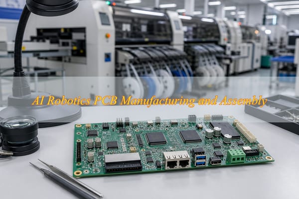
AI robotics PCB manufacturing brings computing, vision, sensing, motion control, communications, and power electronics into one hardware program. A computing board may require dense BGA breakout and controlled impedance, while motor-control and power-distribution boards must carry pulsed current without disturbing sensors or data links.

Prototype success does not guarantee repeat production. Mixed file revisions, unavailable processors, fine-pitch solder defects, motor-related power noise, concentrated heat, and incomplete test limits can cause rework, inconsistent builds, or delayed product validation.

EBest Circuit reviews the complete manufacturing package. We align PCB data, BOM, placement, assembly, programming, inspection, and customer-defined test requirements before production, then support fabrication and assembly from prototype through volume builds. Send your Gerber/ODB++, BOM, quantity, assembly files, and test scope to sales@bestpcbs.com for a free DFM review and quotation.

AI robotics PCB manufacturing, assembled robot controller PCB on an electronics production workbench

What Types of PCBs Are Used in AI Robotics Systems?

Board partitioning should follow system function. An AI robotics system may distribute computing, sensing, motion, power, and communication across several PCBs or combine selected functions on one board. Common PCB categories include:

PCB Type Main Function Typical Requirements
AI computing PCB Runs AI inference, control algorithms, and data processing Dense BGA routing, high-speed interfaces, controlled impedance, thermal management
Vision PCB Connects cameras and image sensors High-speed interfaces, low-noise power, compact layout
Sensor PCB Collects encoder, IMU, force, distance, or environmental data Low-noise analog circuits, stable references, reliable sensor interfaces
Robot control PCB Coordinates motion, I/O, and communications MCU/FPGA integration, CAN/Ethernet interfaces, mixed-signal layout
Motor control PCB Drives BLDC motors, servos, and other actuators Higher current, MOSFET thermal paths, reinforced power connections
Power distribution PCB Converts and distributes battery or DC input power Current-carrying capacity, power connectors, protection devices, thermal control
Communication PCB Handles wired or wireless links Controlled impedance, RF requirements, connector and antenna constraints

A humanoid robot may place motor-control boards close to individual joints while keeping AI computing and vision processing in the head or torso. An autonomous mobile robot may use a central computing board connected to separate motor, navigation, power, and communication boards.

The exact architecture depends on processing load, mechanical space, cable length, current distribution, and serviceability. Before releasing each board, verify its power budget, interface ownership, connector path, mounting envelope, and replacement boundary; an unclear split can create overloaded connectors, duplicated power conversion, or interfaces that cannot be tested independently.

Which Components and Interfaces Are Commonly Used on AI Robot PCBs?

Package mix and interface speed drive PCB complexity. AI robot PCBs may combine processors, memory, sensors, power devices, and communication circuits whose electrical, assembly, and test-access requirements must be reviewed together.

Common components include:

  • AI processors and SoCs: Run computer vision, neural-network inference, navigation, and higher-level decision functions.
  • MCUs and FPGAs: Handle real-time I/O, timing-sensitive control, motion functions, and interface management.
  • DDR memory and flash storage: Support high-bandwidth processing and local data storage.
  • Image sensors and camera-related ICs: Support RGB, depth, stereo, and machine-vision systems.
  • IMUs and motion sensors: Measure acceleration, angular rate, orientation, or movement.
  • Motor drivers and MOSFETs: Switch current for BLDC motors, servos, pumps, and actuators.
  • Encoders and feedback devices: Provide position, speed, and motion feedback.
  • DC-DC converters and regulators: Generate stable power rails for processors, sensors, and communication circuits.

Common interfaces include:

  • CAN and CAN-FD: Connect distributed motor and control nodes.
  • Ethernet: Carries higher-bandwidth data between computing and control modules.
  • USB: Supports peripherals, cameras, configuration, and data transfer.
  • PCIe: Supports high-bandwidth expansion or computing modules where the architecture requires it.
  • High-speed camera interfaces: Carry image and vision data between sensors and processors.
  • Wi-Fi and Bluetooth: Support wireless communication, configuration, and telemetry.

For engineering and sourcing teams, the important cost and schedule drivers are package pitch, routing density, current, and interface speed rather than the total component count. Include these constraints in the RFQ so suppliers quote the required stackup, inspection, and assembly route instead of pricing from board dimensions alone.

Which PCB Technologies Are Needed for AI Processors, Vision Sensors, and Motion Control?

Each robot function owns different PCB requirements. AI processing is dominated by BGA breakout, memory routing, power integrity, and heat; machine vision by low-noise power and camera-link continuity; and motion control by pulsed current, switching loops, protection, and thermal paths.

  • AI processor and memory routing: Start from the released processor escape pattern, DDR topology, interface constraints, and stackup. Use HDI, laser microvias, or filled via-in-pad only when the BGA pitch and routing channels cannot be completed with a simpler through-via structure. Verify impedance coupons where specified and review the routed design for reference-plane continuity and excessive via transitions before fabrication.
  • Processor power integrity: Separate core, memory, I/O, and auxiliary rails according to the processor power tree. Place the required decoupling close to the relevant power balls, provide low-impedance return paths, and size regulator and copper paths for startup and workload transients. Validate rail sequencing, ripple, droop, and current at defined operating states rather than checking only idle voltage.
  • Processor thermal path: Move package heat into the PCB copper, thermal vias, heat spreader, or chassis interface defined by the mechanical design. Confirm thermal-pad solder coverage and interface contact during assembly, then measure component temperature under sustained inference and communication loads to check throttling margin.
  • Vision sensor signal path: Route MIPI, LVDS, USB, Ethernet, or other camera links to their specified impedance, skew, and reference requirements. Maintain a continuous return structure across connectors and layer transitions, and keep camera clocks and data pairs away from motor-switching nodes. Verify the interface with captured images and error monitoring under representative cable length and frame rate.
  • Vision sensor power and grounding: Supply image sensors, clocks, and analog references from low-noise rails with local filtering and decoupling placed at the receiving devices. Keep shared impedance with motor and power-conversion returns out of the sensor reference path. Compare image noise, dropped frames, and sensor data with motors disabled and operating to identify coupling.
  • Motion-control power stage: Size MOSFET, driver, shunt, connector, copper, and plated transitions from continuous current, peak current, duty cycle, and fault-clearing requirements. Keep the switching and gate-drive loops compact, separate sensitive encoder and communication routes, and provide a defined heat path from the power devices. Validate current waveform, rail disturbance, device temperature, and protection response at startup, reversal, braking, stall, and commanded load changes.

Assign each requirement to one board function and one verification method so computing, vision, and motion-control rules are not copied across unrelated boards.

How Should Robot Control PCBs Handle Motor Current, Power Noise, and Signal Integrity?

A robot control PCB must prevent motor and actuator loads from disturbing processors, sensors, and communication circuits. Current changes during motor startup, braking, reversal, and torque changes can create voltage drop, switching noise, and ground disturbance.

  • Current-path sizing: Size power traces and copper areas from both continuous and peak current so the conductors match the actual load.
  • Layer-change capacity: Use sufficient copper and plated connections where current changes layers to avoid narrow current bottlenecks.
  • Switching-loop control: Keep high-current switching loops compact around MOSFETs, motor drivers, and local decoupling to reduce conducted and radiated noise.
  • Power and signal separation: Route motor-current paths away from low-level analog and sensor circuits to reduce measurement disturbance.
  • Return-path continuity: Maintain continuous return paths under high-speed signals so return current does not detour around plane gaps.
  • Bulk energy storage: Place bulk capacitance close to high-current loads to limit supply collapse during rapid load changes.
  • Local high-frequency decoupling: Place local decoupling close to processors, drivers, and interface ICs to reduce high-frequency supply noise.
  • Connector current limit: Check connector current rating together with PCB copper capacity because an undersized connector can become the limiting point.
  • Sensitive-node clearance: Keep switching nodes away from encoder inputs, analog sensors, clocks, and sensitive communication lines.

A controller that operates normally on a bench may reset when several motors accelerate together. Power-rail drop, connector resistance, inadequate bulk capacitance, or poor current return paths should be checked before treating the problem as a processor or firmware failure.

How Are HDI PCBs for AI Robotics Manufactured?

Specify HDI only when the routed design needs it. Engineers should confirm that through vias cannot complete the BGA breakout or high-speed routing. Procurement should compare the proposed microvia structure, lamination count, via fill, registration plan, test evidence, and repeat-production controls.

The released stackup should identify core and prepreg construction, finished copper, dielectric spacing, impedance requirements, microvia layers, and permitted via structures. These inputs let the supplier confirm manufacturability and allow the buyer to see which fabrication steps and inspections are included in the quotation.

  • Microvia structure: State the start and stop layers, finished diameter, pad size, and whether the vias are staggered, stacked, filled, or capped. This prevents different suppliers from quoting different constructions under the same HDI label.
  • Via-in-pad requirement: Identify the BGA, LGA, or thermal-pad locations that require filling and planarization. Ask the supplier to confirm the fill and surface preparation included in the build.
  • Lamination count: Request the proposed build sequence when several drilling and lamination cycles are required. Additional cycles affect cost, lead time, registration risk, and the ease of repeating the design.
  • Fine-line capability: Compare the released trace, space, annular-ring, and registration requirements with the supplier’s reviewed manufacturing limits for this stackup rather than relying on a general capability table.
  • Plating evidence: Define the required finished copper and hole requirements and agree on the coupon, microsection, or inspection evidence needed for lot acceptance.
  • Impedance verification: Provide target values, tolerances, reference layers, and coupon requirements. Request the measured coupon result when controlled impedance is part of the order.
  • Registration review: Ask for a DFM response covering microvia-to-pad alignment and layer-to-layer registration where the design uses tight capture pads or stacked structures.
  • Bare-board release: Include electrical testing for opens and shorts and define any additional dimensional, impedance, or microsection records required before assembly.

Request a reviewed stackup before tooling. If a simpler via structure completes the routing, remove unnecessary lamination cycles, cost, and supply risk.

What Assembly Controls Are Required for AI Processors, BGAs, Memory, and Fine-Pitch Components?

AI robotics PCB manufacturing, microscope inspection of a fine-pitch robot controller PCBA

Fine-pitch packages need an agreed assembly and inspection plan. Engineers should identify package-specific risks, while procurement should confirm which controls and records are included in the quotation for processors, DDR devices, QFNs, LGAs, BGAs, and small passive components.

  • Package-data confirmation: Supply manufacturer part numbers, approved footprints, polarity, and package drawings. Require discrepancies to be raised before stencil or placement-program release.
  • Moisture-sensitive handling: Identify moisture-sensitive devices and request handling records when storage exposure or baking can affect package integrity and solderability.
  • Stencil review: Ask the assembler to review stencil thickness and critical apertures against the complete package mix, especially when a large thermal pad sits beside fine-pitch passives.
  • Paste inspection scope: Define whether SPI is required for the pilot and production lots and which paste defects or trends must stop the build before placement.
  • First-article evidence: Agree on the component identity, polarity, placement, and workmanship checks that must be completed before the balance of the lot proceeds.
  • Reflow confirmation: Request confirmation that the profile is developed around board thermal mass, solder-paste requirements, and component temperature limits.
  • Hidden-joint inspection: Specify X-ray coverage and acceptance criteria for BGA, LGA, QFN, and other bottom-terminated packages that AOI cannot assess.
  • Thermal-pad acceptance: Define how solder coverage or voiding beneath exposed pads will be evaluated when it affects heat transfer or electrical grounding.
  • Mixed-technology assembly: Identify press-fit, selective-soldered, or manually installed power connectors so their tooling, sequence, and inspection are included in the quote.

For a valid price comparison, require each supplier to state the SPI, AOI, X-ray, first-article, programming, and test scope. Before release, confirm that the PCB data, BOM, CPL, assembly drawing, approved alternatives, and firmware identify the same revision.

How Should Thermal Performance Be Managed in AI Robotics PCB Assemblies?

Concentrated heat needs a continuous thermal path. Heat from AI processors, regulators, motor drivers, MOSFETs, and other power devices must move through the package connection, PCB copper and vias, and any heat spreader or enclosure interface defined by the mechanical design.

  • Copper heat spreading: Use larger copper areas around power devices to spread heat beyond the package footprint.
  • Thermal-via path: Add thermal vias beneath exposed thermal pads when heat needs to move into internal or opposite-side copper.
  • Copper selection: Select copper thickness according to actual current and thermal requirements instead of increasing copper across the entire board.
  • Thermal-pad paste control: Control solder paste beneath large thermal pads so excessive voiding does not interrupt the intended heat path.
  • Mechanical heat transfer: Provide heat-sink or chassis contact when the mechanical design uses conductive cooling.
  • Sensor placement: Keep temperature-sensitive sensors away from concentrated heat sources where possible.
  • Thermal interface definition: Define thermal interface material thickness and contact area when the PCB transfers heat to a metal enclosure or heat spreader.
  • Loaded temperature validation: Verify temperature under representative processor and motor loads rather than relying only on idle measurements.

A processor can remain stable during short functional testing and still throttle or fail during sustained inference workloads. Thermal validation therefore needs to reflect the real operating duty cycle.

How Should Vibration and Mechanical Stress Be Controlled in Robotics PCB Assemblies?

Control mechanical loads at their entry and stress points. Vibration, shock, cable movement, connector loading, and repeated motion should be addressed at mounting points, heavy components, connectors, board edges, and flexible interconnects.

  • Mounting-hole placement: Position mounting holes so mechanical loads do not produce excessive board flex around BGAs or other large packages.
  • Heavy-component support: Avoid leaving heavy inductors, transformers, capacitors, or connectors unsupported in high-vibration areas.
  • Connector retention: Use connectors with suitable retention when repeated motion could loosen a friction-fit connection.
  • Cable strain relief: Provide cable strain relief so cable movement is not transferred directly into solder joints.
  • Loaded-connector reinforcement: Reinforce through-hole or mechanically loaded connectors when insertion or cable force justifies it.
  • Stress-zone clearance: Keep mechanically sensitive components away from board edges, mounting stress areas, and enclosure interference zones.
  • Staking or underfill decision: Use staking or underfill only where component mass, vibration, or qualification requirements justify the added process.
  • Coating keep-outs: Define coating keep-out areas before conformal coating when connectors, test points, or thermal contact surfaces must remain exposed.
  • Rigid-flex bend control: When rigid-flex is used, match bend radius, flex length, copper construction, and bend location to the real mechanical movement.

Rigid-flex is a special interconnect option for suitable mechanical structures. It should not be treated as a standard PCB type required by all AI robotics products.

How Are AI Robotics PCB Assemblies Inspected, Programmed, and Functionally Tested?

AI robotics PCB manufacturing, functional test fixture connected to a robot controller PCBA

Buyers need a test plan that connects each risk to evidence. Before ordering, engineering should define the functions and limits that matter, procurement should confirm what the supplier includes, and both teams should agree on the records delivered with the lot. “AOI and functional test included” is not enough unless the coverage and acceptance criteria are stated.

  1. Define bare-board evidence: Require electrical testing for opens and shorts and identify any stackup, dimensional, finish, impedance-coupon, or microsection records needed for acceptance. Procurement can then confirm whether those records are included in the PCB price.
  2. Set paste-control expectations: Identify packages or thermal pads that justify SPI and agree on the defects or trends that stop the line. The supplier should explain how paste results are tied to the released stencil and board revision.
  3. Approve first-article coverage: Specify the identity, polarity, orientation, placement, and visible-joint checks required before the remaining quantity is assembled. Ask for a recorded approval rather than relying on an undocumented operator check.
  4. Request hidden-joint evidence: Map BGA, LGA, QFN, and bottom-terminated pads to X-ray coverage and project acceptance criteria. A representative image is useful only when it identifies the board, package, lot, and decision basis.
  5. Choose unpowered checks: Use ICT, flying probe, or a dedicated fixture only where test access and circuit behavior support useful limits. Engineering should define which nets, values, or rail resistances can distinguish an assembly fault from normal component tolerance.
  6. Control firmware identity: Provide the approved bootloader, MCU, FPGA, or configuration package with tool settings and a version or checksum. Require the programming result to be linked to the lot or serial number when traceability matters.
  7. Define functional acceptance: State input voltage, power sequence, interfaces, loads or simulators, expected responses, and pass/fail limits. Request measured values for critical functions instead of accepting a record that only says “powered on.”
  8. Agree on failure handling: Define which test records accompany the lot and how failures, rework, and retest are logged. This prevents repeated testing from hiding intermittent faults and gives engineering data for corrective action.

Engineering can build the functional-test scope from the board’s released interfaces and system risks:

  • Power acceptance: State startup sequence, rail limits, expected current, reset behavior, and abnormal-current response at defined input conditions.
  • Communication acceptance: Name each CAN, CAN-FD, Ethernet, USB, or other interface, together with the messages, speed, termination, and error criteria to be exercised.
  • Sensor and encoder acceptance: Provide known input states or simulator signals, expected readings, range limits, and fault responses.
  • Motor-output acceptance: Define enable, direction, PWM or command response, feedback, protection behavior, and the safe load or simulator used at PCBA level.
  • Vision-interface acceptance: Define camera detection, link mode, frame transfer, and error reporting; reserve optical alignment and final image-quality acceptance for the assembled robot where appropriate.
  • Service-function acceptance: Identify programming ports, storage, GPIO, indicators, and service interfaces that must work before the PCBA is shipped.

Separate PCBA acceptance from robot-level validation. Put the boundary in the purchase specification: the supplier can release the assembled board against agreed electrical and functional limits, while motion accuracy, navigation, sustained system thermal loading, full actuator performance, optical alignment, safety behavior, and final-product EMC remain system-level responsibilities unless separately contracted.

What Common Problems Cause AI Robot PCB Prototypes to Fail?

Combined loads reveal failures missed by power-on checks. Motors, processors, sensors, cameras, and communication interfaces can create simultaneous electrical and thermal conditions that do not appear when each function is checked separately.

  • Reset during motor startup: Check rail droop, bulk capacitance, regulator response, connector resistance, and motor-current return paths.
  • Unstable sensor readings: Check sensor grounding, reference supplies, switching-node proximity, and routing near analog or encoder signals.
  • Camera or interface errors: Check impedance, pair routing, return paths, connector pinout, layer transitions, and assembly quality.
  • Processor overheating: Check package power, exposed-pad soldering, thermal vias, heat spreading, heat-sink contact, and enclosure cooling.
  • Intermittent BGA faults: Review X-ray results, reflow data, package handling, and board warpage before treating the fault as software-related.
  • Connector faults during movement: Check retention, solder support, cable strain, board flex, and enclosure interference.
  • Build-to-build inconsistency: Compare the PCB, stackup, BOM, manufacturer part numbers, firmware, assembly files, and test procedure by revision.

Convert an effective prototype rework into an approved design or process change before the next build.

How Do You Move an AI Robotics PCB from Prototype to Mass Production?

Engineering and procurement should release one production baseline. A working prototype is not enough for a repeat order. The purchase package must connect approved design data, components, firmware, inspection, test limits, deviations, and commercial scope to one revision.

Use the following customer-side release checklist before authorizing volume production:

  1. Approve one PCB baseline: Release the PCB revision, stackup, Gerber/ODB++, drill data, fabrication drawing, and impedance requirements together. Put the same revision identifier on the purchase order and supplier acknowledgement.
  2. Close DFM questions: Assign an owner and disposition to BGA breakout, microvia, current-path, panel, clearance, paste, and mechanical issues before approving tooling or a stencil.
  3. Approve the production BOM: Confirm manufacturer part numbers, allowed alternatives, do-not-substitute items, moisture sensitivity, and programming requirements. Procurement should not accept a substitution until engineering evaluates its electrical, thermal, mechanical, firmware, and qualification effects.
  4. Match assembly files: Check that the BOM, CPL, assembly drawings, polarity data, special-process notes, and board data belong to the same release. Send one controlled package rather than separate email attachments with uncertain revisions.
  5. Agree on process evidence: Confirm which SPI, first-article, AOI, X-ray, soldering, and workmanship records the supplier will create and which records the customer will receive or may review.
  6. Release programming files: Provide firmware, bootloader, configuration, tool settings, and the required version or checksum record. State whether traceability is by lot, panel, or individual serial number.
  7. Set acceptance limits: Define the defects and limits covered by visual inspection, AOI, X-ray, electrical checks, and functional testing. Do not leave acceptance to an unspecified factory default.
  8. Approve the test package: Release power limits, sequencing, interfaces, loads, fixtures, software, expected responses, and pass/fail criteria. Where practical, challenge the station with known-good and known-fault conditions before relying on its results.
  9. Review the pilot build: Compare the intended materials, programs, tooling, inspection, and test flow with what was actually used. Close deviations, rework trends, and test escapes through documented actions.
  10. Authorize volume release: Approve the updated package only after pilot findings are closed and the accepted first-article and test evidence represent the intended production configuration.

During pilot review, check paste variation, fixture access, connector insertion, thermal-pad consistency, rework trends, and test cycle practicality. Repeat orders should reference the approved baseline and require disclosure of material, component, process, firmware, or test changes.

What Should You Look for in an AI Robotics PCB Manufacturer and Assembly Partner?

Choose a partner by risk closure and evidence. An AI robotics PCB manufacturer should connect bare-board fabrication, component sourcing, assembly, programming, inspection, and test to the customer’s released requirements rather than quote each operation in isolation.

Before placing an order, compare suppliers on these customer-facing commitments:

  • Reviewed manufacturing proposal: Request a stackup, via structure, copper construction, panel approach, and DFM response tied to the actual design.
  • Comparable quotation scope: Confirm whether tooling, stencil, component sourcing, programming, SPI, AOI, X-ray, electrical test, functional test, packaging, and records are included or excluded.
  • Controlled component sourcing: Require purchasing by manufacturer part number and written approval before any alternative is used.
  • Package-specific inspection: Map fine-pitch and hidden-joint packages to the inspection method and acceptance criteria that will be applied.
  • Programming traceability: Agree on firmware identity, programming records, and the lot-level or serial-level traceability needed by the project.
  • Pilot-to-volume continuity: Confirm how approved materials, programs, tooling, deviations, and test limits will carry from prototypes into repeat orders.
  • Failure and change disclosure: Define how nonconforming results, rework, substitutions, and process changes will be reported before shipment or reuse.

A supplier response that names these deliverables gives engineering a technical review path and gives procurement a comparable commercial baseline. If the quotation leaves them undefined, later tooling, sourcing, inspection, or acceptance changes can create avoidable cost and schedule risk.

Why Choose EBest Circuit for AI Robotics PCB Manufacturing and Assembly?

One controlled project package reduces manufacturing handoffs. EBest Circuit coordinates fabrication, sourcing, assembly, inspection, and test preparation, giving engineering and purchasing teams one manufacturing contact from prototype verification through repeat production.

  • Free DFM review: Identify stackup, via, footprint, panel, and assembly conflicts before tooling, reducing avoidable prototype rework.
  • Prototype-to-production continuity: Keep approved PCB data, BOM revisions, assembly programs, and inspection requirements aligned as volumes increase.
  • HDI and fine-pitch support: Match BGA breakout, via-in-pad, controlled impedance, and assembly controls to the released design instead of applying unnecessary complexity.
  • Component sourcing control: Purchase against manufacturer part numbers and approved alternatives, helping prevent unapproved substitutions and BOM drift.
  • Inspection matched to package risk: Combine bare-board electrical test, SPI, AOI, and X-ray where each method can detect the relevant defect class.
  • Programming and functional-test support: Build around your controlled firmware, procedures, fixtures, and pass/fail limits so delivered evidence matches your acceptance plan.

What Files Are Needed for an AI Robotics PCB and PCBA Quote?

A quotation must define the complete manufacturing scope. PCB construction, component sourcing, assembly work, programming, and testing affect the manufacturing route. Missing inputs can make the initial price incomplete.

For AI robotics PCB manufacturing, provide:

  • PCB image data: Gerber or ODB++ files.
  • Drill data: NC drill files.
  • Fabrication drawing: PCB fabrication drawing.
  • Stackup definition: Defined stackup, if available.
  • Impedance specification: Controlled-impedance requirements.
  • Copper specification: Copper requirements.
  • Surface finish: Surface finish.
  • Order quantity: Order quantity.
  • Special structures: Special via or mechanical requirements.

For AI robotics PCB assembly, also provide:

  • Production BOM: BOM with manufacturer part numbers.
  • Placement data: CPL or Pick-and-Place file.
  • Assembly drawing: Assembly drawing.
  • Component alternatives: Approved component alternatives.
  • Programming package: Firmware or programming files when required.
  • Functional-test procedure: Functional-test procedure.
  • Test fixture: Test fixture information, if available.
  • Protective materials: Conformal-coating or underfill requirements when specified.
  • Packaging and labeling: Packaging and labeling requirements.

Gerber files do not define sourcing, placement, programming, or functional testing. Send the available package so missing quotation inputs can be identified before order release.

FAQs About AI Robotics PCB Manufacturing and Assembly

Q1: Can an AI robotics PCBA combine SMT, through-hole, and press-fit components?
A1: Yes. Mixed assembly can combine SMT devices, through-hole connectors, and press-fit components when the PCB hole tolerances, assembly sequence, and mechanical requirements are defined before production.

Q2: How should irregular robot PCBs be panelized for assembly?
A2: Panelization should provide enough support for printing, placement, reflow, inspection, and depanelization. Irregular outlines may require breakaway rails, routing tabs, or dedicated tooling so the PCB remains stable during SMT production.

Q3: Can customer-supplied AI processors or computing modules be used for assembly?
A3: Yes. Consigned components can be used when the component identity and handling condition are confirmed against the BOM, supplied quantity, packaging, and moisture status before assembly.

Q4: How are ESD-sensitive sensors and processors handled during PCBA production?
A4: ESD-sensitive parts should remain within an ESD-controlled handling process, including suitable workstations, storage, transport, grounding, and packaging according to the component requirements.

Q5: Can serial numbers or QR codes be added to robotics PCB assemblies?
A5: Yes. Serial numbers, labels, or QR codes can be linked to production lots, PCB revisions, assembly records, or test results when traceability is required.

Q6: How should board-to-board and cable connectors be selected for repeated mating cycles?
A6: Connector selection should verify mating life, retention, electrical load, and mechanical fit against the expected vibration, signal speed, cable strain, and available installation space. The PCB footprint alone does not determine connector suitability.

Q7: Can robotics PCBA production use lead-free soldering?
A7: Yes. Lead-free assembly is widely used when the PCB finish, components, solder alloy, and reflow profile are compatible with the required process.

Q8: How should assembled AI robotics PCBs be packed before shipment?
A8: Packaging should control ESD, mechanical, contamination, and moisture risks. The selected tray, bag, cushioning, and outer carton should match component sensitivity, connector exposure, board size, and shipment conditions.

Q9: What information is needed to quote a functional test?
A9: Provide the test conditions, interfaces, limits, and fixture status, together with the applicable software or scripts and expected responses. If the fixture is not yet available, identify which checks belong to PCBA production and which remain at final robot integration.

Q10: When should a pilot build be repeated before mass production?
A10: Repeat the pilot after a released design, process, firmware, test, or interface change whenever the existing build evidence no longer represents the intended production configuration.

Conclusion

Repeatability depends on one approved baseline. Keep PCB construction, components, assembly, firmware, inspection, and test limits aligned across repeat orders.

EBest Circuit can review your AI robotics PCB manufacturing package from prototype planning through repeat production. Submit the released manufacturing package: Gerber/ODB++, BOM, CPL, assembly drawing, quantity, programming package, and applicable test requirements. Email sales@bestpcbs.com for a free DFM review and quotation.

You may also like

OAM PCB Explained: How It Works in AI Servers

August 21st, 2026

OAM PCB is the accelerator-module circuit board used to connect high-density AI compute with a server's power, high-speed links, management, and cooling systems. OAM means OCP Accelerator Module; the module normally works with a Universal Base Board (UBB) rather than operating as a stand-alone processor board. This guide shows how the parts fit together, how OAM differs from SXM, and which electrical, thermal, mechanical, fabrication, and assembly requirements matter to a buyer.

EBest Circuit (Best Technology) supports AI accelerator PCB projects with high-layer and HDI fabrication, controlled impedance, component sourcing, BGA assembly, AOI, X-ray inspection, and customer-defined test coordination. If you are evaluating an OAM PCB, send your current board requirements to sales@bestpcbs.com for an initial manufacturability discussion.

OAM PCB
OAM accelerator PCB module in an AI server platform.

What Is an OAM PCB?

An OAM PCB is the printed circuit board used in an OCP Accelerator Module. It carries an AI accelerator device and the supporting circuitry required to power, manage, connect, and cool that device inside a compatible server platform.

  • Compute: a GPU, ASIC, NPU, FPGA, or another parallel processor.
  • Local support: memory, voltage regulation, clocks, management devices, and sensors.
  • System connection: the connector and mechanical interfaces that link the module to a compatible baseboard and cooling assembly.

OAM defines a form factor and interface framework, not a processor brand or a fixed PCB construction. The actual layer count, materials, vias, components, and tests still depend on the accelerator, power envelope, cooling approach, UBB, and product specification.

How Does an OAM PCB Work in an AI Server?

Inside an AI server, the OAM PCB acts as the local platform for one accelerator. It receives power and management connections from the system, provides the short electrical paths needed around the accelerator and memory, and connects high-speed links to the UBB.

The UBB brings multiple OAM modules together. It distributes power and management signals and provides the physical interconnect fabric between accelerators. Depending on the system architecture, those accelerator-to-accelerator links can support the very high data movement needed for training or inference workloads.

A simplified data path is:

  • The host server sends work and data toward the accelerator platform.
  • The UBB routes high-speed links, power, and control connections to each OAM module.
  • The OAM PCB supports the accelerator, local memory, power conversion, sensing, and module-level interfaces.
  • Cooling hardware removes heat from the accelerator and other high-power components.

This division lets the module, baseboard, host, power system, and cooling system be developed as coordinated building blocks. It also means an OAM PCB cannot be evaluated in isolation: its connector geometry, mounting features, power inputs, thermal stack, and high-speed interfaces must match the intended platform.

What Does the OAM Architecture Include?

Although implementations vary, the OAM architecture normally combines several functional groups on one dense PCB.

  • Accelerator package: the main GPU, ASIC, NPU, FPGA, or other compute device.
  • Local memory: high-bandwidth or other memory devices placed close to the accelerator when required by the processor architecture.
  • Power delivery: voltage regulators, inductors, capacitors, current sensing, and power-control circuits that convert the module input into multiple low-voltage rails.
  • High-speed interfaces: differential channels connecting the accelerator to other modules, the host, and management resources through the module connector.
  • Management and monitoring: controllers, EEPROMs, clocks, temperature sensors, voltage monitors, and service interfaces.
  • Mechanical and thermal interfaces: mounting holes, keep-out areas, stiffeners, heatsink contact zones, and the flatness needed for reliable connector engagement and cooling contact.

These groups compete for board area and influence one another. A larger power stage changes copper distribution and thermal behavior. Dense high-speed escape routing can require HDI structures. A heavy heatsink can increase mechanical loading. The architecture must therefore be translated into one coordinated stackup, layout, fabrication, assembly, and cooling plan.

How Do OAM Modules and UBBs Work Together?

An OAM module is the accelerator board; a UBB is the baseboard that hosts and connects multiple modules. The two boards perform different jobs but operate as one platform.

Platform part Primary role What must match
OAM module Carries one accelerator and its local support circuits. Connector, power, lane map, cooling, and mounting.
UBB Hosts and links multiple OAM modules. Sockets, routing, current capacity, management, and clearances.
AI server Combines compute, power, cooling, firmware, and software. Power sequence, thermal capacity, service access, and validation.

A useful way to picture the relationship is: AI server -> UBB -> multiple OAM modules -> accelerator and local memory on each module.

For example, when eight accelerator modules are installed on one UBB, a connector-position error on one OAM PCB can prevent reliable mating, while an incorrect lane map or channel-loss assumption can affect communication beyond that single module. The OAM and UBB suppliers therefore need controlled interface drawings and the same revision baseline.

OAM PCB
Eight OAM modules connect through a UBB inside an AI server tray.

OAM vs SXM: What Is the Difference?

OAM and SXM are both used for high-performance accelerator modules, but they come from different platform ecosystems. OAM is associated with the Open Compute Project and is intended to support an open, multi-vendor infrastructure. SXM is a proprietary NVIDIA module format used in selected NVIDIA server platforms.

Decision area OAM SXM
Ecosystem Open, OCP/OAI-oriented. Proprietary NVIDIA platform.
Choose when The system uses an OAM-compatible accelerator and UBB. The selected NVIDIA platform requires SXM.
Baseboard OAM-compatible UBB. Designated NVIDIA baseboard.
Can they swap? No; the complete platform must match. No; the complete platform must match.

The two formats should not be treated as drop-in replacements. Moving a design from one to the other can affect the module PCB, baseboard, firmware, cooling assembly, power delivery, chassis, and system validation. The form-factor decision belongs at the platform architecture stage, before PCB fabrication data is released.

What Are the PCB Design Requirements for OAM-Compatible Systems?

An OAM-compatible system must carry fast signals, high current, dense packages, and substantial thermal and mechanical loads at the same time. The PCB design requirements are therefore interconnected.

  • Stackup and materials must support the required channel loss, impedance, layer count, thickness, and fabrication capability.
  • Differential pairs need controlled geometry, continuous reference planes, suitable spacing, and a via strategy that limits discontinuities.
  • Large packages and dense connectors may require blind or buried vias, microvias, via-in-pad, filled vias, and back drilling.
  • Power and ground structures must carry the module current while controlling voltage drop, noise, and localized heating.
  • Copper distribution and layer construction must support board flatness and reduce assembly warpage risk.
  • Connector footprints, mounting holes, heatsink interfaces, keep-outs, and board edges must follow the mechanical definition of the target platform.

The most useful design review looks at the complete path: accelerator package breakout, on-module routing, connector launch, UBB routing, and the destination device. A locally correct trace can still fail if the combined channel exceeds its loss or discontinuity budget.

What Power and Thermal Requirements Shape an OAM PCB?

OAM PCBs combine high power density with strict mechanical and signal-integrity requirements. Power and thermal design therefore shape the physical PCB, not just the component selection.

Requirement group What shapes the PCB What the customer must define
Power Planes, copper, vias, decoupling, and regulator layout. Input power, rail current, voltage drop, transients, and sequence.
Thermal Heat spreading, component spacing, and cooler interface. Cooling method, contact area, temperature limits, and test conditions.
Mechanical Thickness, stiffeners, mounting, alignment, and flatness. Datums, mounting load, keep-outs, tolerances, and tray limits.

These requirements must be reviewed together. More copper may improve current capacity but can change etching, lamination, impedance geometry, flatness, and reflow behavior. A large cooling assembly may remove heat effectively but still create board strain if the mounting stack is not coordinated.

The PCB manufacturer can review manufacturability and material implications, but final power integrity, cooling design, and server validation remain system responsibilities.

How Are PCBs Fabricated and Assembled for OAM Modules?

OAM modules are commonly advanced multilayer assemblies, but the exact process should follow the released design rather than a generic OAM recipe.

  • Fabrication review: confirm materials, copper, impedance geometry, via structure, lamination, registration, back drilling, thickness, flatness, and finish.
  • Assembly planning: account for large BGAs, memory, power components, connector coplanarity, thermal mass, moisture control, paste, placement, and reflow.
  • Verification plan: select bare-board electrical test, impedance testing, SPI, AOI, X-ray, dimensional checks, and customer-defined functional tests according to the real risks.

No single inspection method proves the whole module. The evidence plan should match the likely failure modes and the test points that are actually accessible.

EBest Circuit (Best Technology) can support manufacturability review, material coordination, PCB fabrication, component sourcing, BGA assembly, AOI, X-ray inspection, and customer-defined testing coordination. Accelerator architecture, firmware, system cooling, regulatory compliance, and final server qualification remain with the customer and its platform partners.

OAM PCB
Inspection of a high-density OAM PCB assembly in an electronics laboratory.

Where Is OAM PCB Technology Used?

OAM PCB technology is used where systems need dense, modular accelerator computing. The most visible applications are AI training servers and high-performance computing platforms, but the same infrastructure can also support inference, data analytics, scientific computing, and other workloads built around compatible accelerator modules.

  • AI training servers that need several tightly connected accelerator modules.
  • High-performance computing clusters handling scientific or engineering workloads.
  • Cloud and enterprise AI infrastructure designed around serviceable accelerator trays.
  • Inference and data-analytics platforms that benefit from dense modular compute.
  • Specialized compute appliances built around an OAM-compatible accelerator ecosystem.

OAM is not automatically the best format for every AI product. PCIe cards may be simpler for lower-power or broadly compatible add-in acceleration, while embedded modules may fit edge systems with tighter space and power limits. OAM becomes most relevant when the platform benefits from high accelerator density, strong module-to-module communication, serviceable modular hardware, and coordinated power and cooling.

How to Choose an OAM PCB Manufacturer?

An OAM PCB manufacturer should be evaluated against the released board requirements, not against a generic list of advanced capabilities.

Evaluation stage What to confirm Why it matters
1. Platform fit Understands the OAM/UBB interface and board requirements. Prevents interface assumptions from reaching production.
2. Process fit Covers the required HDI, impedance, assembly, and inspection steps. Keeps fabrication and assembly decisions aligned.
3. Build control Controls material, stackup, BOM, files, and test revisions. Reduces prototype-to-production revision drift.

The best supplier is not necessarily the one that claims the highest layer count. It is the one that can explain how the specific OAM design will be built, where its process margins are tight, what evidence will be delivered, and which responsibilities remain with the system developer.

For project-specific review, send the released Gerber or ODB++ data, stackup, fabrication drawing, BOM, placement data, assembly drawing, connector and mechanical definitions, and test requirements to sales@bestpcbs.com.

FAQs About OAM PCB

What does OAM mean in PCB hardware?

OAM means OCP Accelerator Module. In PCB hardware, it describes an accelerator-module form factor and interface framework developed in the Open Compute Project ecosystem.

Is an OAM PCB the same as a UBB?

No. The OAM PCB carries one accelerator module. The Universal Base Board hosts and connects multiple OAM modules and provides shared interconnect, power, management, and mechanical integration.

Is OAM the same as NVIDIA SXM?

No. Both are accelerator-module formats, but OAM belongs to an open OCP/OAI ecosystem while SXM is a proprietary NVIDIA platform. Their interfaces and system requirements are not interchangeable.

Why are OAM PCBs difficult to manufacture?

They can combine high layer counts, low-loss materials, HDI vias, dense high-speed routing, high-current power structures, large BGA packages, strict flatness, and demanding thermal hardware on one assembly.

What should be reviewed before building an OAM PCB?

Review the platform specification, board and UBB revisions, stackup, impedance and loss targets, via structure, power inputs, connector and mechanical definitions, thermal stack, BOM, assembly data, and inspection and test requirements.

Planning an OAM PCB or another AI accelerator PCB? Send your current design package or project questions to sales@bestpcbs.com. EBest Circuit (Best Technology) can review the PCB fabrication, sourcing, assembly, inspection, and customer-defined test scope for your build.
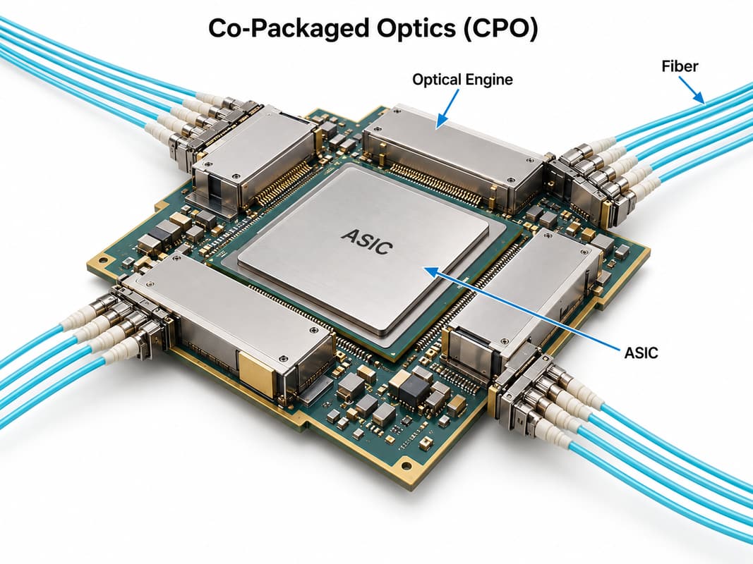
You may also like

UBB PCB (Universal Baseboard): Manufacturing Guide for AI Accelerators

August 20th, 2026

A UBB PCB is the large, high-speed Universal Baseboard that connects multiple AI accelerator modules. For AI accelerators, its signal paths, power distribution, connector accuracy, and mechanical fit directly affect whether the system can be assembled and operated reliably. Even if a board passes a basic open/short test, incorrect impedance, voltage drop, connector alignment, or flatness can still cause unstable links, poor contact, overheating, or tray interference.

EBest Circuit (Best Technology) supports complex multilayer and HDI PCB manufacturability review, controlled-impedance fabrication, agreed sourcing and PCBA, inspection, and test coordination from prototype through production. System architecture and final platform validation remain with the customer. Planning a UBB PCB build? Send your stackup, fabrication data, drawings, impedance requirements, quantity, and assembly scope to sales@bestpcbs.com for an engineering and quotation review.

UBB PCB
UBB PCB connecting multiple accelerator module positions on one large baseboard.

What Is a UBB PCB?

A UBB PCB is the Universal Baseboard that carries and connects multiple OAM accelerator modules in an AI computing platform. It acts as the common electrical and mechanical foundation between the accelerator modules and the rest of the system.

Its main roles include:

  • Module connection: provides defined locations and interfaces for OAM modules.
  • High-speed interconnect: carries host and module-to-module data paths.
  • Power distribution: delivers the required power domains to accelerator modules and supporting circuits.
  • Management support: routes clock, reset, monitoring, debug, and other sideband signals.
  • Mechanical integration: aligns the modules with the host interface, power hardware, tray, and cooling system.

The UBB is not the accelerator module itself. The OAM carries the accelerator device and local circuitry; the UBB connects several modules into one platform. The applicable OCP/OAI revision and final production files determine the actual implementation.

How Does a UBB PCB Connect OAM Modules?

A UBB PCB connects OAM modules through precisely located high-density interfaces. In simple terms, the relationship is: OAM modules → UBB PCB → host, power, and management interfaces. Reliable operation also depends on mechanical compatibility with the tray and cooling hardware.

Four interfaces must agree:

  • OAM-to-UBB: connector footprint, pad geometry, mating height, keep-outs, and module position.
  • UBB-to-host: host-interface lanes, clocks, resets, and other control signals.
  • UBB-to-power system: power connector locations, voltage domains, current paths, and standby rails.
  • UBB-to-chassis: board outline, mounting holes, tray features, cooling clearance, and service access.

A connector can be electrically correct but mechanically unusable if hole locations, flatness, or mating clearance drift. Before fabrication, confirm the OAM, host interface board, power distribution board, tray, and cooling drawings use the same controlled revision.

What Are the Key UBB PCB Specifications?

A UBB PCB does not have one universal layer count, thickness, material, or copper construction. However, UBB designs usually share several manufacturing characteristics because they must connect multiple OAM modules on one large electrical and mechanical platform.

Typical characteristic Why it matters on a UBB PCB
Large format Fits multiple OAM, host, power, and mounting interfaces.
High layer count Provides routing, reference planes, and power layers.
Low-loss construction Supports long accelerator signal paths.
Controlled impedance Preserves critical signal geometry.
Complex vias/backdrill Enables dense routing and limits via stubs.
High-current copper Carries module power through planes and vias.
Mechanical control Maintains flatness, alignment, and module fit.

These are common UBB PCB characteristics, not fixed values. The released platform specification and fabrication package must define the actual board outline, finished thickness, layer construction, materials, copper weights, impedance targets, via structures, backdrill limits, connector requirements, and flatness tolerances.

Why Is UBB PCB Manufacturing So Challenging?

UBB PCB manufacturing is challenging because one large baseboard must support several OAM interfaces, long high-speed channels, high-current structures, and strict module-to-tray alignment at the same time. Each requirement is demanding on its own; their interaction on the same board creates the distinctive UBB manufacturing risk.

The main manufacturing risks are:

  • Multiple OAM interfaces: connector fields must remain aligned with every module position across a large board.
  • Long high-speed channels: material behavior, impedance geometry, vias, and backdrill accuracy accumulate across extended routes.
  • High-current and fine-signal features: heavy power copper and precise signal geometry need compatible lamination, imaging, etching, and plating controls.
  • Large-board flatness: copper imbalance or material movement can affect module seating, connector engagement, and tray installation.
  • Late-stage yield exposure: a hidden lamination, plating, registration, or dimensional defect can scrap the complete multi-module baseboard.

The key difficulty is therefore not simply making a high-layer-count PCB. It is keeping signal, power, and mechanical requirements within tolerance across the entire UBB after repeated lamination, drilling, plating, and thermal processes.

What Stackup and Materials Are Used for UBB PCBs?

A UBB stackup normally has to satisfy three competing requirements: low-loss signal transmission, high-current power distribution, and dimensional stability across a large board. This is why UBB material selection cannot be separated from layer construction, copper balance, via design, and finished thickness.

A practical UBB stackup usually combines:

  • High-speed signal layers: low-loss laminate, controlled dielectric thickness, suitable copper profile, and adjacent reference planes support long accelerator interconnects.
  • Power and ground layers: multiple plane layers and appropriate copper weights distribute module current while providing stable signal return paths.
  • Routing and transition structures: through vias, blind or buried vias, via-in-pad, and backdrilling may be combined where OAM escape density or stub control requires them.
  • Balanced construction: symmetric materials and copper distribution help control bow, twist, thickness, and connector coplanarity on the large baseboard.

Low-loss materials are important because UBB channels can cross a substantial portion of the baseboard and pass through several via or connector transitions. These low-loss materials must also remain compatible with the selected copper, lamination cycle, and mechanical requirements. Heavy copper helps power delivery but can make etching, resin filling, lamination, and warpage control more difficult. The approved production stackup must balance both needs rather than optimizing either one in isolation.

A material brand alone does not define performance. The production stackup should state the actual dielectric system, glass style, copper profile, dielectric thickness, copper weights, impedance geometry, and permitted material alternatives.

UBB PCB
Stackup, material, via, and backdrill review for a complex UBB PCB.

How Does a UBB PCB Handle High-Speed Signals?

A UBB PCB handles high-speed signals by preserving controlled geometry and reference-plane continuity across long routes between multiple module and system interfaces. Because a UBB can combine extended traces with several via and connector transitions, small manufacturing deviations can accumulate into greater channel discontinuity or loss. Manufacturing must therefore reproduce the customer's validated materials, traces, vias, antipads, and residual stubs.

Evidence to request from the PCB manufacturer includes:

  • An approved production stackup with the actual impedance geometry.
  • Controlled differential-pair width, spacing, copper compensation, and reference planes.
  • Backdrill depth and residual-stub control where required by the channel design.
  • Registration checks for connector pads, vias, antipads, and plane clearances.
  • Lot-linked impedance coupons and TDR (time-domain reflectometry) results.

TDR confirms the manufactured impedance structure; it does not prove the complete system channel. The customer validates signal integrity, while the manufacturer provides fabrication records that can be compared with simulation and platform results.

How Does a UBB PCB Handle High-Power Distribution?

A UBB PCB handles high-power distribution by reproducing the customer's defined power paths through power connectors or press-fit interfaces, copper planes, neck-down regions, plated vias, and via arrays. The fabrication task is to preserve the specified copper cross-section and geometry from each power entry to the relevant module interfaces.

The most important PCB manufacturing features are:

  • Copper construction: specified foil and plated copper thickness must be achieved on planes, traces, and finished holes.
  • Plane and neck-down geometry: local restrictions near connectors, cutouts, or dense signal regions must not reduce the intended current path.
  • Via arrays: finished hole size, plating thickness, via count, and spacing determine the available vertical copper cross-section.
  • Power connector holes: drilled diameter, plating, positional tolerance, and press-fit requirements must match the released connector drawing.
  • Heavy-copper lamination: resin filling, copper balance, and material flow must be controlled to avoid voids, thickness variation, and warpage.

These features influence resistance, voltage drop, temperature rise, and mechanical reliability, but the manufacturer does not replace the customer's power-integrity design. EBest reviews whether the released copper, hole, plating, and material requirements are manufacturable and provides the agreed copper records, microsections, dimensional results, or electrical tests for acceptance.

How Should a UBB PCB Be Inspected and Tested?

A UBB PCB should be inspected with a risk-based plan that covers internal circuitry, vias, impedance, dimensions, mechanical fit, and—when assembly is included—hidden solder joints and customer-defined functional checks.

Ask for evidence that answers these customer questions:

  • Was the approved material and stackup used? Review material and stackup records.
  • Were circuit defects detected before lamination or shipment? Review internal and external AOI results.
  • Will the board fit the modules and tray? Check the outline, connectors, mounting holes, thickness, and flatness report.
  • Are hidden vias and backdrills acceptable? Review microsections for plating, resin fill, lamination, and residual stubs.
  • Does the bare board match the netlist? Require 100% continuity and isolation testing.
  • Was controlled impedance achieved? Review lot-linked TDR coupon results.
  • Are hidden assembly joints acceptable? Use AOI or X-ray where the PCBA risk requires it.
  • Does the assembled board meet the agreed function? Use customer-defined fixtures and pass/fail limits.

Decide before ordering which records are required for prototypes and which must accompany every production lot. EBest can coordinate the required inspection records and keep them tied to the correct lot and file revision.

UBB PCB
Dimensional and electrical inspection of a large UBB PCB.

How to Choose a UBB PCB Manufacturer?

Choose a UBB PCB manufacturer by checking whether its real process capability, engineering response, verification evidence, and production controls match your released board—not by accepting a generic multilayer-PCB claim.

Ask four customer-focused questions:

  • Can they build it? Match board size, thickness, materials, HDI/via construction, backdrill, impedance, and power features.
  • Can they explain the risks before quoting? Expect clear questions about stackup, drill pairs, copper balance, tolerances, and substitutions.
  • Can they prove what they inspected? Define electrical test, TDR, microsections, dimensions, AOI/X-ray, and lot records.
  • Can they repeat the process in production? Confirm material continuity, revision control, critical processes, and production inspection.

A representative sourcing problem occurs when a large UBB is quoted only by layer count and quantity. If material construction, board size, backdrill, impedance reporting, and flatness are clarified after the order, the price, lead time, or yield expectation can change. A better supplier resolves these items before the build and records every approved exception.

EBest Circuit can review controlled fabrication data, stackup, drill files, drawings, impedance requirements, quantities, and the agreed PCBA/test scope. Our role is to identify manufacturing gaps early, build to the approved package, and provide the agreed evidence for customer acceptance.

FAQs About UBB PCB

Is a UBB PCB the same as an OAM module?

No. The UBB is the shared baseboard that connects multiple OAM modules. An OAM is the accelerator module installed into the UBB interface.

Does every UBB PCB use the same layer count and material?

No. Stackup, materials, copper, vias, and thickness depend on the platform's signal, power, mechanical, and manufacturing requirements.

Does an OCP UBB specification replace the production files?

No. It provides an architecture and interface reference. Manufacturing still requires final fabrication data, drawings, stackup, drill files, materials, and acceptance criteria.

What should be tested before a UBB PCB is assembled?

Confirm the stackup, dimensions, continuity, isolation, critical vias, impedance, flatness, and connector locations before assembly.

What files should I send for a UBB PCB quotation?

Send the fabrication data, drill files, approved or target stackup, impedance requirements, material notes, mechanical drawings, acceptance criteria, revision, quantities, and—if needed—BOM, placement, assembly, and test files.

Need a UBB PCB manufacturing review? Send your final files, quantities, and PCB/PCBA requirements to sales@bestpcbs.com. EBest Circuit will identify open manufacturing questions and confirm the next steps before production.
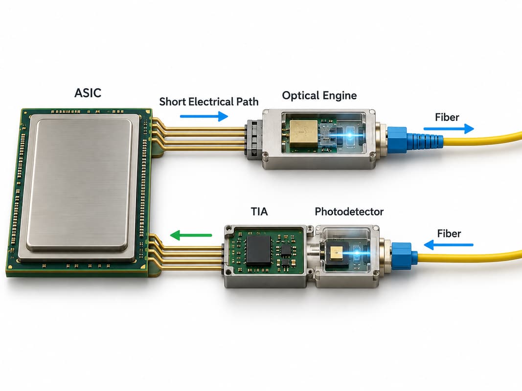
You may also like

Practical AI Accelerator PCB Manufacturing Guide

August 20th, 2026

AI accelerator PCB combines fast data channels, high current, dense packages, and demanding thermal interfaces on one board. A weakness in the stackup, via structure, material choice, assembly process, or inspection plan can cause signal loss, unstable power, solder defects, overheating, or an expensive redesign.

EBest Circuit (Best Technology) supports these projects from manufacturability review and material coordination through PCB fabrication, component sourcing, BGA assembly, X-ray inspection, and customer-defined testing. Keeping these stages with one manufacturing partner helps maintain the same revision, stackup, component, and quality requirements from prototype to repeat production.

If you are preparing an AI accelerator PCB for quotation or production, send your Gerber data, stackup, BOM, assembly files, and test requirements to sales@bestpcbs.com for a project-specific review.

AI accelerator PCB
AI accelerator PCB manufacturing for high-speed computing hardware.

What Is an AI Accelerator PCB?

An AI accelerator PCB is the circuit board that carries or connects specialized processors used to accelerate artificial-intelligence workloads. The processor may be a GPU, NPU, ASIC, FPGA, or another dedicated computing device.

The PCB provides the physical platform for:

  • High-speed connections to the host, memory, and other accelerators.
  • Stable power for the processor, memory, and supporting circuits.
  • Management, clock, control, and communication devices.
  • Mechanical attachment to connectors, stiffeners, heatsinks, and the enclosure.
  • Component assembly, inspection, programming, and testing.

Depending on the system, the product may be a PCIe accelerator card, an embedded AI module, an OAM-style module, a carrier or baseboard, or a custom computing assembly. The PCB is not the accelerator chip itself; it is the high-density electrical and mechanical foundation that allows the accelerator to operate inside the finished product.

What Are the Key Requirements for AI Accelerator PCBs?

An effective AI accelerator PCB must handle high-speed data, high current, dense interconnection, thermal stress, and reliable assembly at the same time.

The main requirements are:

  • Controlled high-speed channels: The stackup, impedance, routing layers, vias, and connectors must support the customer’s channel targets.
  • Stable power delivery: Power and ground structures must carry the required current without excessive voltage drop or localized heating.
  • Suitable PCB materials: Laminates, copper profiles, and dielectric thicknesses must match signal-loss, thermal, mechanical, availability, and cost needs.
  • High-density routing: Fine-pitch devices and connectors may require HDI, blind or buried vias, via-in-pad, or back drilling.
  • Thermal and mechanical compatibility: Board thickness, copper distribution, mounting holes, stiffeners, and heatsink interfaces must work together.
  • Repeatable PCBA: Stencil design, component handling, placement, reflow, warpage control, and inspection must suit large or fine-pitch packages.
  • Defined quality evidence: Bare-board tests, AOI, X-ray, electrical tests, and functional tests should match the risks of the product.

These requirements are interdependent. Increasing copper for power, for example, can change etching, lamination, impedance geometry, reflow behavior, and board flatness. The best result comes from reviewing the complete board rather than treating each specification separately.

Why Are AI Accelerator PCBs Difficult to Manufacture?

AI accelerator PCBs are difficult to manufacture because several advanced features often appear on the same board, leaving less room for process variation.

Common combinations that increase difficulty include:

  • Many signal, power, and ground layers in a controlled finished thickness.
  • Low-loss materials combined with fine traces and tight impedance control.
  • Blind, buried, stacked, filled, or back-drilled vias.
  • Dense accelerator, memory, and connector breakout areas.
  • Large copper areas next to fine-pitch circuitry.
  • Large BGAs or modules with high thermal mass and warpage sensitivity.

A thicker multilayer board may improve routing and power distribution but make small-hole plating more difficult. Thin HDI dielectrics may improve package escape but require additional lamination cycles. Heavy copper can carry more current but may affect copper balance, etching, and assembly heat.

The challenge is therefore not simply producing one advanced feature. It is controlling registration, plating, lamination, impedance, flatness, and assembly when all those features interact. Early engineering review helps identify which combination is likely to control yield, cost, and lead time before material is committed.

What Stackup and Materials Are Used for AI Accelerator PCBs?

AI accelerator PCBs typically use multilayer or HDI stackups with dedicated signal, reference, power, and ground layers. The exact construction depends on channel length, interface speed, routing density, power demand, via architecture, board thickness, and mechanical form factor.

A practical stackup may include:

  • Signal layers placed next to continuous reference planes.
  • Closely coupled power and ground layers where required by the power-integrity design.
  • HDI build-up layers for dense package or connector escape.
  • Mechanically drilled through-holes for lower-density connections and structural strength.
  • Back drilling where unused plated-through-hole stubs would create excessive signal discontinuity.

Low-loss materials are often used for long or fast channels, while hybrid stackups may place higher-performance material only where it provides a clear electrical benefit. Material selection should consider more than a published Dk or Df value.

DecisionCustomer priorityManufacturing effect
Signal layersLoss and impedanceLayer count and dielectric geometry
Power layersCurrent and voltage dropCopper weight and balance
Via structurePackage escape and stub limitsDrill and lamination sequence
LaminateElectrical and thermal needsAvailability, processing, and cost
ThicknessConnector and mechanical fitStackup tolerance and flatness

The production stackup should identify actual materials, dielectric thicknesses, finished copper, via structures, controlled impedances, and tolerances. If the fabricator proposes a material or geometry change, the customer’s electrical owner should evaluate its effect before the design is built.

AI accelerator PCB
Multilayer stackup, low-loss materials, and controlled interconnect structures.

What High-Speed Requirements Affect AI Accelerator PCB Manufacturing?

High-speed requirements affect material selection, stackup geometry, copper profile, impedance control, via design, back drilling, and fabrication tolerances.

Three areas deserve particular attention:

  • Channel loss: Laminate loss, copper roughness, trace length, and via transitions determine how much of the signal reaches the receiver.
  • Impedance discontinuity: Neck-downs, antipads, connectors, layer changes, and unused via stubs can create reflections.
  • Skew and crosstalk: Pair geometry, reference planes, glass weave, spacing, and routing consistency affect timing and noise.

The fabrication drawing should clearly identify controlled-impedance structures, target values and tolerances, coupon requirements, and any back-drill or residual-stub limits. The fabricator should calculate impedance using the proposed production materials and finished copper rather than generic design values.

TDR coupon results can show whether selected structures meet the agreed impedance requirement. They do not replace the customer’s full-channel simulation, eye-diagram analysis, or protocol validation. The manufacturing value is consistency: the built geometry and test evidence should match the approved stackup.

What Power Requirements Affect AI Accelerator PCB Manufacturing?

AI accelerator PCB manufacturing must support high current, rapid load changes, low-voltage rails, and concentrated heat without creating excessive voltage drop or unreliable copper structures.

Board-level power affects:

  • The number and location of power and ground layers.
  • Copper weight, plane shape, neck-down areas, and connector transitions.
  • The quantity and arrangement of power and thermal vias.
  • Decoupling-component placement and available routing space.
  • PCB thickness, copper balance, flatness, and assembly heat.
  • Heatsink, stiffener, mounting, and airflow interfaces.

Even a short narrow section in a high-current path can create voltage drop and local heating. Likewise, adding heavy copper without considering balance can make fabrication and reflow less uniform. Power integrity therefore needs to be translated into practical plane geometry, copper construction, and via structures before the stackup is finalized.

EBest Circuit can review whether the released copper, via, material, and mechanical features are manufacturable. The customer or its design partner remains responsible for load assumptions, voltage-drop limits, simulation targets, and final cooling-system performance.

Why Is HDI Important for AI Accelerator PCBs?

HDI is important because dense accelerator packages and high-pin-count connectors can require smaller vias and more routing space than conventional through-hole structures provide.

HDI can help by:

  • Escaping fine-pitch packages with shorter, smaller interconnects.
  • Keeping through-holes from blocking multiple inner routing layers.
  • Providing more direct access to power and ground structures.
  • Reducing the electrical length of selected layer transitions.
  • Supporting compact modules and dense connector areas.

However, HDI should not be added simply because the product is an AI board. Blind microvias, stacked structures, via-in-pad, copper filling, and repeated sequential lamination increase cost and process sensitivity. A staggered structure or a combination of microvias and mechanically drilled vias may be more practical when routing allows it.

The objective is the least complex via architecture that still meets package escape, signal, power, reliability, thickness, and cost requirements. Microvia depth, diameter, land size, stacking, filling, registration, and reliability expectations should be reviewed as one structure.

What Makes AI Accelerator PCB Assembly Difficult?

AI accelerator PCB assembly is difficult because large devices, fine-pitch joints, high component density, heavy copper, and uneven thermal mass must pass through one stable assembly process.

Major assembly risks include:

  • BGA warpage: A large package and the PCB may bend differently during reflow, increasing open-joint or head-in-pillow risk.
  • Hidden solder joints: BGAs and bottom-terminated devices cannot be fully assessed by visual inspection alone.
  • Uneven heating: Heavy copper, large ground areas, connectors, and heatsinks can create different heating and cooling rates.
  • Paste-volume conflict: Fine-pitch devices and large thermal pads may require different stencil strategies.
  • Moisture exposure: Improper storage or handling of moisture-sensitive devices can damage packages during reflow.
  • Mechanical loading: Stiffeners, heatsinks, and mounting hardware can stress the assembled board if their sequence or torque is not controlled.

Consider an accelerator card with a large BGA, low-loss multilayer PCB, back-drilled high-speed vias, and high-current power stages. If the stackup changes after electrical approval, or the reflow plan ignores board and package warpage, the prototype may pass continuity testing yet fail under load or temperature cycling.

For this type of project, EBest Circuit can coordinate the approved BOM, component handling, stencil review, placement, reflow, AOI, X-ray, and customer-defined test steps under one revision-controlled build. Programming files, functional limits, fixtures, and final product acceptance requirements should be supplied or approved by the customer.

AI accelerator PCB
BGA assembly and X-ray inspection for an AI accelerator PCB.

How Are AI Accelerator PCBs Inspected and Tested?

AI accelerator PCBs are inspected in stages because bare-board defects, placement errors, hidden solder joints, and functional failures require different methods.

Bare PCB inspection

  • AOI checks the patterned layers for selected opens, shorts, and image defects.
  • Electrical testing checks network continuity and isolation.
  • Impedance coupons and TDR verify agreed controlled structures.
  • Dimensional or microsection records may be added when specified.

Assembly inspection

  • SPI can check solder-paste deposition when included in the inspection plan.
  • AOI checks component presence, position, polarity, and visible solder joints.
  • X-ray examines hidden BGA and bottom-terminated solder joints.
  • First-article records confirm the approved revision and assembly condition.

Electrical and functional testing

  • ICT or boundary scan can detect defined assembly and connectivity faults.
  • Programming verification confirms that the specified device image was loaded.
  • Fixture-based functional tests check customer-defined operating conditions.
  • Burn-in or environmental screening is used only when the project specification requires it.

No single result proves the complete product. Before production, the customer and supplier should agree which reports are required, how sampling will work, what constitutes acceptance, and how failures will be handled. This avoids receiving a stack of inspection reports that does not answer the product’s real risks.

How to Choose an AI Accelerator PCB Manufacturer?

Choose an AI accelerator PCB manufacturer by checking whether it can control the complete combination of stackup, materials, HDI features, assembly risks, and quality evidence required by your board.

Ask each candidate to provide:

  • A producible stackup with named materials and realistic alternatives.
  • DFM feedback on the features most likely to affect yield or reliability.
  • A clear plan for impedance control, HDI, back drilling, copper balance, and board flatness where applicable.
  • BGA assembly, moisture handling, warpage, reflow, AOI, and X-ray controls.
  • Component sourcing and traceability controls for PCBA orders.
  • Defined test methods, sampling, acceptance criteria, and report outputs.
  • A revision-control process covering quotation, fabrication, assembly, programming, and testing.

EBest Circuit’s advantage is the ability to connect these stages rather than treating the PCB, components, assembly, and inspection as unrelated purchases. One engineering and production path can help reduce stackup mismatches, uncontrolled material substitutions, BOM revision errors, and gaps between assembly risk and inspection evidence.

Send the same controlled data package to each supplier so quotations are comparable. A useful quotation should identify the material system, stackup assumptions, special processes, tooling, inspection, test scope, lead-time conditions, and unresolved questions—not only a headline price.

FAQs About AI Accelerator PCB

What files are needed for an AI accelerator PCB quotation? Provide Gerber or approved fabrication data, a fabrication drawing, drill files, stackup or impedance requirements, dimensions, tolerances, quantity, and schedule. For assembly, also provide the BOM, centroid data, assembly drawings, approved substitutions, programming needs, and test requirements.

Can one supplier handle both AI accelerator PCB fabrication and assembly? Yes, if the supplier has the required fabrication, sourcing, assembly, inspection, and test capabilities. Using one coordinated partner can reduce revision mismatches between the bare PCB and PCBA stages.

How are large BGA solder joints inspected? AOI checks visible placement and surrounding joints, while X-ray is used for hidden BGA connections. Acceptance criteria should be defined for the package, board, and product rather than inferred from an image alone.

Can an alternative low-loss laminate be used? Sometimes, but it should be evaluated for dielectric properties, copper profile, available thicknesses, thermal behavior, process compatibility, lead time, and its effect on the approved impedance and loss model.

What affects AI accelerator PCB prototype cost and lead time? The main drivers include layer count, material availability, HDI and lamination cycles, via filling, back drilling, impedance requirements, board size, copper weight, component availability, assembly complexity, inspection, testing, quantity, and engineering review.

A reliable AI accelerator PCB depends on the stackup, high-speed channels, power delivery, HDI structure, assembly process, and inspection plan working together. EBest Circuit (Best Technology) can support the project from manufacturability review and PCB fabrication through sourcing, BGA assembly, X-ray inspection, and customer-defined testing.

Send your fabrication data, stackup, BOM, and test requirements to sales@bestpcbs.com for a project-specific AI accelerator PCB review and quotation.

You may also like

Artificial Intelligence in PCB Assembly Optimization

August 20th, 2026

Artificial intelligence in PCB assembly optimization is becoming more practical as SMT lines generate increasing amounts of production and inspection data. SPI, placement machines, reflow ovens, AOI, X-ray inspection, testing, and traceability systems all provide information that can be used to identify process patterns. AI helps connect these data points, allowing engineers to detect abnormalities earlier and investigate why defects occur rather than only where they are found.

For PCB assembly buyers, the real value is better process control, inspection, and yield—not AI for its own sake. EBest Circuit supports PCB fabrication, PCBA assembly, and box-build projects from prototypes to volume production. If your project has demanding assembly, inspection, testing, or traceability requirements, send your Gerber files, BOM, and assembly requirements to sales@bestpcbs.com for an engineering review.

artificial intelligence in pcb assembly optimization

What Is AI in PCB Assembly?

AI in PCB assembly refers to the use of machine learning, computer vision, pattern recognition, and data analytics to support manufacturing decisions.

Traditional PCB assembly relies on machine programs, process limits, SPC, inspection rules, and engineering experience. AI adds another layer by analyzing larger volumes of production data and identifying relationships between different process variables.

For example, an AOI defect may be linked to solder paste volume, placement offset, component geometry, or reflow conditions. Instead of examining each stage separately, AI can help correlate these records.

Typical applications include:

  • defect recognition and classification;
  • AOI and X-ray image analysis;
  • SMT process optimization;
  • yield analysis;
  • process drift detection;
  • root-cause analysis.

AI is therefore most useful when it works alongside established process controls and manufacturing engineering rather than replacing them.

artificial intelligence in pcb assembly optimization

How Is AI Used in PCB Assembly?

AI can be applied across several stages of PCB assembly because each stage produces different types of manufacturing data.

Typical sources include:

  • SPI: solder paste height, area, volume, and offset;
  • Placement: coordinates, corrections, feeder and nozzle data;
  • Reflow: temperature profiles, zone settings, and conveyor speed;
  • Inspection: AOI images, X-ray images, and defect records;
  • Testing: ICT, functional test, and failure results;
  • Traceability: PCB serial numbers, material lots, machines, and production history.

The key advantage comes from connecting these records.

If AOI repeatedly finds insufficient solder on the same package, engineers can compare those failures with earlier SPI, placement, and reflow data. This shifts the investigation from where a defect was detected toward which upstream condition may have contributed to it.

That cross-process visibility is one of the main ways AI can support PCB assembly optimization.

How Does AI Optimize the SMT Assembly Process?

AI can help engineers analyze relationships between solder paste printing, placement, reflow, and downstream inspection results.

Solder Paste Printing

  • SPI data can reveal changes in paste volume, height, area, or offset. When these measurements are compared with later defects, engineers can identify patterns that deserve attention.

Component Placement

  • Placement data can reveal repeated corrections associated with a particular component, feeder, nozzle, or board location. Instead of treating each adjustment as an isolated event, historical data can show whether the pattern is becoming systematic.

Reflow Soldering

  • AI can compare production results with variables such as zone temperature, conveyor speed, package size, and board characteristics. This can help engineers narrow down process combinations associated with recurring soldering problems.

The objective is not to replace thermal profiling or process engineering. It is to use historical production data more effectively so engineers can investigate potential causes and make process adjustments with better evidence.

How Does AI Improve PCB Assembly Inspection?

Inspection is one of the most practical areas for AI in PCB assembly because modern inspection equipment already generates large amounts of image and measurement data.

AOI

AOI may inspect conditions such as:

  • missing or misplaced components;
  • polarity errors;
  • solder bridges;
  • insufficient solder;
  • lifted leads;
  • abnormal solder-joint appearance.

Machine-learning models can help distinguish actual defects from acceptable process variation. This is particularly useful when conventional inspection rules generate excessive false calls.

X-Ray Inspection

AI can also support X-ray analysis for hidden solder joints under BGA, QFN, and other bottom-terminated packages. Typical inspection targets include voiding, bridging, insufficient solder, alignment issues, and hidden joint abnormalities.

The practical benefit is not simply detecting more features. Better classification can reduce unnecessary review while making inspection results more useful for upstream process correction.

How Does AI Detect PCB Assembly Defects?

AI-based defect detection commonly uses computer vision or measurement data to recognize patterns associated with known assembly defects.

Depending on the inspection method, these may include:

  • missing components;
  • component shift;
  • reversed polarity;
  • tombstoning;
  • solder bridges;
  • insufficient solder;
  • lifted leads;
  • hidden solder-joint abnormalities.

A trained model can compare new inspection data with previously classified examples and estimate whether a condition represents normal variation or a genuine defect.

AI can also help group repeated failures. If the same defect appears on one reference designator, package type, component lot, or production line, the pattern becomes easier to identify.

However, reliable detection still depends on representative training data and consistent defect classification. AI can improve the speed of analysis, but inspection criteria and engineering validation remain essential.

How Does AI Improve PCB Assembly Yield?

AI can support PCB assembly yield improvement by connecting defect results with the process conditions that occurred earlier in production.

Instead of looking only at the final yield percentage, engineers can compare failures with:

  • SPI measurements;
  • placement corrections;
  • reflow conditions;
  • AOI or X-ray results;
  • component lots;
  • repair records;
  • electrical test failures.

This can make recurring failure patterns easier to identify.

First-Pass Yield

First-pass yield is particularly useful because repeated inspection, repair, and retesting add time and handling to the assembly process. AI-based analysis can help engineers focus on process variables that show a strong relationship with recurring defects.

Root-Cause Analysis

Connected production data can also reduce the time needed to trace a defect back through earlier processes.

For example:

AOI detects a solder defect → SPI history shows abnormal paste variation → engineers inspect stencil or printing conditions.

The practical goal is straightforward: identify problems earlier and shorten the path from defect detection to corrective action.

What Data Does AI Need for PCB Assembly Optimization?

Useful AI analysis depends more on data quality and traceability than simply collecting a large quantity of data.

Common inputs include:

  • SPI measurements;
  • placement and correction records;
  • reflow parameters;
  • AOI and X-ray results;
  • defect classifications;
  • rework records;
  • ICT and functional test results;
  • PCB serial numbers;
  • component lot information;
  • machine and production timestamps.

Traceability is especially important. If a failed board cannot be connected to its earlier manufacturing history, root-cause analysis becomes much harder.

Consistent labeling also matters. Similar defects should not be recorded under several unrelated names if the data will later be used for model training or statistical analysis.

For many manufacturers, improving data structure is therefore an important first step before introducing more advanced AI tools. Good manufacturing data gives both AI systems and engineers a stronger basis for decision-making.

What Are the Challenges of Using AI in PCB Assembly?

One challenge is high-mix production. An EMS factory may assemble many PCB designs with different packages, materials, volumes, and inspection requirements. A model that performs well on one product may require adjustment for another.

Other practical issues include:

  • inconsistent data formats between equipment;
  • limited historical data for prototypes or low-volume builds;
  • false positives and missed defects;
  • process changes after material or equipment adjustments;
  • inconsistent defect labeling.

AI also identifies correlations, which are not always the same as root causes. A change in defect rate may coincide with a reflow adjustment, for example, while the actual cause is related to solder paste, PCB design, component condition, or another variable.

For this reason, AI works best as an engineering support tool.

The most reliable approach combines production data, AI analysis, established process controls, and manufacturing engineering judgment.

FAQs About Artificial Intelligence in PCB Assembly Optimization

Can AI completely automate PCB assembly optimization?

Not in most production environments. AI can assist with inspection, process analysis, prediction, and troubleshooting, while engineers still validate process changes and product-specific requirements.

What PCB assembly data can AI analyze?

AI can analyze SPI measurements, placement data, reflow records, AOI and X-ray images, defect history, rework records, traceability information, and electrical test results.

Can AI reduce PCB assembly defects?

AI can identify patterns associated with recurring defects and help engineers detect abnormal process trends earlier. Actual defect reduction comes from applying appropriate corrective actions based on those findings.

Is AI suitable for low-volume PCB assembly?

Yes, although the approach may differ from mass production. Low-volume projects may have less product-specific historical data, so generalized inspection models, cross-product data, and engineering rules become more important.

How is AI different from traditional PCB assembly process control?

Traditional process control relies on defined limits, machine settings, SPC, inspection criteria, and engineering experience. AI adds pattern recognition and predictive analysis across larger datasets. In practice, the two approaches complement each other.

artificial intelligence in pcb assembly optimization

If you are developing a PCB or PCBA project and need support with assembly process control, inspection, testing, or traceability, EBest Circuit can review your manufacturing files before production. Send your Gerber files, BOM, assembly drawings, test requirements, and expected quantity to sales@bestpcbs.com so our team can evaluate the project and prepare an appropriate manufacturing and quotation plan.

You may also like

Custom Servo Driver Board Manufacturing and PCB Assembly for AI Robot Hardware

August 14th, 2026

A servo driver board turns an AI robot controller’s motion commands into stable, synchronized actuator movement. A reliable custom design must match the servo interface, simultaneous current demand, control timing, connector system, PCB layout and test strategy; a simple bank of headers is not enough.

The scope covers PWM and serial-bus servo interfaces for robot hardware. Industrial AC servo drives require a separate motor-specific power-stage and control design.

Servo driver board for multi-axis AI robot hardware on a laboratory workbench

What Is a Servo Driver Board in AI Robot Hardware?

A servo driver board connects the robot processor, power source and servo actuators. Its exact role depends on the actuator and command architecture.

Its core functions are to distribute power, route or generate control signals, monitor required feedback and provide the necessary protection and connectors.

This interface must control timing, supply stability, contact reliability and logic integrity. The robot processor cannot correct these board-level failures after they occur.

How Does a Servo Driver Board Control Robot Motion?

The board converts a position, velocity or torque request into the electrical command format expected by each actuator. For a PWM servo, command timing encodes the requested position. For an addressed serial servo, a data packet identifies the actuator and target. Closed-loop industrial drives add current and feedback processing, so they require a different power and control architecture.

Evaluate the complete path under coordinated load; a single unloaded servo will not expose bus timing errors, voltage sag or corrupted feedback.

  • Deterministic updates: Schedule channel updates so simultaneous joints do not receive stale or irregular commands.
  • Safe startup: Hold outputs in a defined state until power rails, firmware and communication are ready.
  • Fault containment: Prevent one shorted cable or failed actuator from disabling unrelated control electronics when required by the system safety analysis.
  • Feedback integrity: Keep encoder, current, temperature and status paths away from noisy power switching loops.

How Do You Choose a Servo Driver Board for a Multi-Axis AI Robot?

Choose the board architecture from the actuator interface, peak simultaneous load and required motion coordination. Channel count by itself is not enough. Two boards with the same number of outputs can behave very differently when several joints accelerate together, when cables are long, or when the robot must recover safely after a fault.

Document these seven inputs before selecting the circuit architecture or connector count:

  • Actuator compatibility: Record every servo part number, supply range, command protocol, logic level and pinout. Confirm the interface from the actuator datasheet and, where possible, a known-good signal capture; a connector match alone does not prove electrical compatibility.
  • Axis count and update timing: Define the installed channels, axes that move together, required update period and worst-case bus latency. A board with enough outputs can still produce visible jitter if commands are delayed or updated unevenly.
  • Simultaneous power demand: Base the input rail, branch distribution and connector current rating on the real acceleration, reversal and holding profile. Normal running current can hide the short peaks that cause brownouts, resets or overheated contacts.
  • Feedback and diagnostics: Specify whether the controller needs position, current, temperature, status or fault data from each actuator. Confirm the required bandwidth and response to missing or invalid feedback before choosing a one-way PWM or bidirectional bus architecture.
  • Cable and connector limits: Control the mating part, pin sequence, wire gauge, cable length, retention method and mating-cycle requirement. These details affect voltage drop, signal integrity, serviceability and resistance to intermittent contact.
  • Startup and fault behavior: Define the output state during power-up, reset, undervoltage, overcurrent, watchdog timeout and communication loss. Decide whether one failed actuator or cable must remain isolated from the controller and other axes.
  • Mechanical and test integration: Check board outline, mounting, enclosure airflow, connector access, programming method and test-point access. Verify measurement and service access in the installed robot, because bench access may hide enclosure constraints.

Why Do Multiple Servos Jitter or Reset the Robot Controller?

Multi-servo jitter and controller resets usually begin with supply droop, shared return impedance, irregular command timing or EMI coupling. Diagnose these causes at the board while reproducing the loaded motion, not by replacing firmware or adding capacitors at random.

  • Reproduce the event: Run the exact joint combination, acceleration and mechanical load that causes the fault.
  • Measure at the load: Capture minimum rail voltage and transient duration at local connectors or test points with adequate bandwidth.
  • Correlate timing: Capture supply voltage, reset, command signal and fault output on the same time base.
  • Separate causes: Repeat with one actuator at a time, reduced acceleration and an alternate cable route to distinguish load current from coupling.
  • Verify the repair: Re-run the worst-case motion across the intended input-voltage and temperature conditions.

Also inspect shared connector pins, thin ground traces and long harness returns; transient current through these impedances can shift the local logic reference and trigger a reset.

How Should Power Integrity Be Designed for a Multi-Servo Driver Board?

Size and verify every element from the power source to the servo connector and return path under simultaneous motion. Use the real motion profile rather than channel count alone.

  • Model simultaneous current: Add the servos that can operate together, controller current and design margin; use stall current only for a credible operating or fault state.
  • Budget voltage drop: Calculate each source, protection, connector, copper, via, cable and return segment with Vdrop = I × R, then measure at the loaded connector.
  • Bulk energy: Place appropriately rated bulk capacitance where the servo rail enters and where a branch experiences a fast load step.
  • Local decoupling: Use the values specified by each controller, transceiver and power-device manufacturer, with short connections to the relevant supply and return pins.
  • Low-impedance distribution: Use copper geometry, layer transitions and connector contacts that match the calculated current and allowable temperature rise.
  • Rail separation: Keep noisy actuator current from flowing through the logic regulator’s sensitive supply and return path.
  • Protection coordination: Select reverse-polarity, surge, overcurrent and branch protection for the available source energy and credible harness faults.
  • Copper and stackup: Select FR4 copper weight and distribution from current, temperature rise, voltage drop and routing density; confirm spacing, vias, escape routing and manufacturability.

How Do PCB Layout, EMI and Thermal Design Affect Servo Board Reliability?

Coordinate switching-loop geometry, return paths, noise control and heat flow during PCB layout. One filter cannot correct poor routing after the layout is complete.

  • Shrink critical loops: Keep the source, switching device, load path, decoupling capacitor and return loop compact.
  • Preserve return paths: Avoid routing that cuts the reference plane beneath clocks, buses and sensitive measurements.
  • Partition by function: Separate power switching, logic, analog sensing and external interfaces while providing deliberate connection points between their returns.
  • Control coupling: Increase separation from noisy nodes, reduce long parallel runs and protect high-impedance signals.
  • Build a thermal path: Connect exposed pads to continuous copper and an appropriate thermal-via pattern, then measure the assembled board under the worst credible motion profile.
  • Record thermal conditions: Log input voltage, active channels, mechanical load, airflow, enclosure state, ambient temperature and soak time with every temperature result.

Compare component and board hot spots with the applicable device limits, derating policy and robot duty cycle.

How Does a Custom Servo Driver Board Prototype Validate Robot Performance?

Validate the prototype under representative multi-axis load; one unloaded servo is not sufficient release evidence. Use six verification gates:

  1. Design for observation: Add safe access to input, servo and logic rails, ground, reset, communication, command outputs and current measurement.
  2. Verify static safety: Check shorts, polarity and rail resistance, then perform the first power-up with a current-limited supply before connecting actuators.
  3. Validate one channel: Confirm signal format, connector pinout, direction, range and fault behavior with one known actuator.
  4. Increase concurrency: Add channels according to the real robot motion profile while logging minimum rail voltage, current and timing.
  5. Apply mechanical load: Test acceleration, reversal, holding and collision-recovery states that change actuator current.
  6. Record release evidence: Save waveforms, temperatures, firmware version, board revision, actuator list and pass limits.

What Must Be Controlled During Servo Driver Board PCB Assembly?

Assembly control must protect component identity, polarity, solder quality, connector alignment and thermal-pad integrity. Servo boards often combine fine-pitch logic, large capacitors, power packages and mechanically loaded connectors, so one uniform inspection method is insufficient.

Servo driver board PCB assembly undergoing automated optical inspection
  • BOM control: Lock manufacturer part numbers, approved alternates, package, ratings and do-not-substitute items.
  • Moisture handling: Follow the component and packaging requirements for moisture-sensitive devices before reflow.
  • Paste and reflow control: Match stencil apertures and the validated thermal profile to the component mix and exposed pads.
  • Polarity inspection: Verify diodes, electrolytic capacitors, IC orientation and connector pin-one features against controlled drawings.
  • Joint inspection: Use AOI for visible placement and solder features, then add X-ray where hidden joints or thermal pads create a real risk.
  • Connector mechanics: Check coplanarity, retention, insertion clearance and any hand-soldered or press-fit operation before functional test.
  • Revision control: Release matching fabrication, BOM, centroid and assembly files under one revision identifier.
  • Programming control: Define the image, checksum, security state, connector, fixture and pass record before assembly release.

Which Functional Tests Should Validate an AI Robot Servo Control Board?

Functional testing should verify power, every channel, communication, protection and loaded motion behavior against written limits. A power-on LED is only an initial observation; it does not prove channel timing, voltage margin or fault recovery.

AI robot servo control board functional testing with multiple servo actuators
Test Method
Input and rails Measure startup, steady state and worst-case transient at defined test points
All output channels Exercise each connector with a known load or validated simulator
Communication Test valid frames, timeout, missing device and bus recovery
Protection Apply controlled undervoltage, overload or disconnected-load conditions where safe
Loaded motion Run representative concurrent trajectories and mechanical loads
Programming and identity Read firmware, configuration, serial-number or revision identifiers

Set limits from actuator data, the control budget, safety analysis and system requirements. Use a protected fixture or simulator for unsafe fault tests and document its coverage limits.

How Do You Move a Servo Driver Board from Prototype to Production?

Release the design only after the board definition, approved parts, assembly controls and measurable acceptance limits are ready for repeat production. Confirm all eight requirements:

  1. Close prototype findings: Assign every electrical, thermal, communication and mechanical failure a root cause, corrective action and passing retest. Update the schematic, layout, BOM and firmware together so the released files match the tested board.
  2. Complete PCB DFM: Review the approved stackup, copper distribution, minimum geometry, drill and via structure, board outline, connector clearances, panelization and fabrication notes against the chosen manufacturer’s documented capabilities.
  3. Complete assembly and test DFM: Confirm package footprints, polarity marks, stencil requirements, fiducials, tool clearance, programming access and test-point size and spacing. The fixture must reach every required rail, interface and output without stressing connectors.
  4. Qualify the production BOM: Lock manufacturer part numbers for controllers, power devices, capacitors and connectors. Evaluate an alternate for electrical rating, pinout, package, thermal behavior, startup behavior and firmware compatibility before approval.
  5. Freeze production inputs: Issue matching Gerber or ODB++, drill, stackup, fabrication notes, BOM, centroid, assembly drawings, firmware image, programming instructions and functional-test specification under one revision.
  6. Build a production-intent pilot: Use the planned PCB construction, approved components, stencil, reflow process, programming method and test fixture. Temporary prototype wiring, hand-selected parts or laboratory-only setup must not hide transfer risks.
  7. Review pilot results: Classify fabrication, placement, soldering, programming and functional-test failures. Record rework and retest results, then verify rail voltage, timing, temperature and loaded multi-axis behavior against written limits before increasing quantity.
  8. Control post-release changes: Link every component, PCB, process, firmware or fixture change to an approval record and an affected-test plan. Repeat only the tests justified by the impact analysis, but never accept generic replacement equivalence without verification.

Why Choose EBest for Custom Servo Driver Board Manufacturing?

Reduce engineering handoffs, identify production risks earlier and keep the approved board and BOM aligned from prototype through repeat builds. These EBest Circuit services address those needs:

  • Resolve board-level risks before ordering volume: PCB design support can review power distribution, stackup, routing, connector placement and test access against the servo interface and motion-load requirements.
  • Validate the design with lower commitment: PCB prototyping and assembly services enable verification builds before the design moves to mass production.
  • Reduce uncontrolled BOM changes: Component sourcing and PCB assembly can work from the same approved manufacturer part numbers and flag alternatives that require engineering confirmation.
  • Match the PCB construction to the electrical load: EBest’s product scope includes FR4, multilayer, heavy-copper, high-Tg and impedance-controlled PCBs for project-specific stackup review.
  • Simplify prototype-to-production transfer: PCB design, prototype, sourcing, assembly and mass-production services can use one controlled set of fabrication, BOM, programming and test files.
  • Support supplier qualification: Use a defined PCB assembly manufacturer selection process to confirm sourcing responsibility, inspection, testing, traceability and change control. EBest lists IATF 16949, ISO 9001:2015, ISO 13485:2016, AS9100D, REACH, RoHS and UL credentials; confirm the certification and product-level documentation required for the specific robot program during quotation.

FAQs About Servo Driver Boards

Q1: What files should I send for a custom servo driver board quotation?

A1: Send the complete fabrication and assembly package. Include Gerber or ODB++, drill files, BOM, centroid data, assembly drawings, quantity, stackup, servo models, protocol, voltage, simultaneous-motion requirement, firmware method and functional test limits.

Q2: Can EBest assemble a customer-designed servo control PCB?

A2: Yes, EBest can fabricate and assemble a customer-designed board. The files still need engineering review for manufacturability, component availability and test readiness before release.

Q3: Can firmware be programmed during PCB assembly?

A3: Programming can be included with controlled inputs. Provide the firmware image, programming interface, security instructions and verification method, including the checksum or version readback that proves the correct image was loaded.

Q4: Does EBest provide a free DFM review before quotation?

A4: Yes, EBest offers a free DFM review for the submitted PCB and assembly package. The review can identify manufacturability issues involving stackup, copper geometry, drill and via choices, component footprints, assembly clearances and test access before production.

Q5: Which PCB constructions can be reviewed for a servo driver board?

A5: The appropriate construction depends on current, thermal, signal and mechanical requirements. EBest’s product scope includes FR4, multilayer, heavy-copper, high-Tg and impedance-controlled PCBs for project-specific review.

Q6: Can EBest support both bare PCB fabrication and complete PCB assembly?

A6: Yes, the service scope includes PCB fabrication, component sourcing and PCB assembly. Define whether the quotation requires bare boards, assembled boards, programming, functional testing or a combination of these services.

Q7: Which quality or compliance credentials should buyers confirm?

A7: Match the required certification or compliance document to the product and end-use program. EBest lists IATF 16949, ISO 9001:2015, ISO 13485:2016, AS9100D, REACH, RoHS and UL credentials; request the applicable current documentation during supplier qualification.

Q8: When is conformal coating appropriate for a robot servo board?

A8: Use conformal coating only when the environmental risk justifies it. Specify keep-out areas, connectors, test points and rework requirements; coating cannot compensate for inadequate spacing or enclosure design.

Q9: What information helps EBest provide a useful DFM review?

A9: Submit the manufacturing files together with the application’s electrical limits. Include Gerber or ODB++, stackup, BOM, centroid data, assembly drawings, servo models, voltage, simultaneous-load profile, connector constraints and required tests.

Q10: What records can accompany a servo driver board shipment?

A10: Define shipment records in the purchase specification. Request the inspection, programming, functional-test and traceability records needed for receiving acceptance before the order is released.

Conclusion

Ready to reduce manufacturing risk before ordering your servo driver board? Send your Gerber or ODB++, BOM, quantity, stackup, servo interface, simultaneous-load profile, assembly, programming and test requirements to sales@bestpcbs.com. Ask EBest for a free DFM review and quotation for your AI robot hardware project.
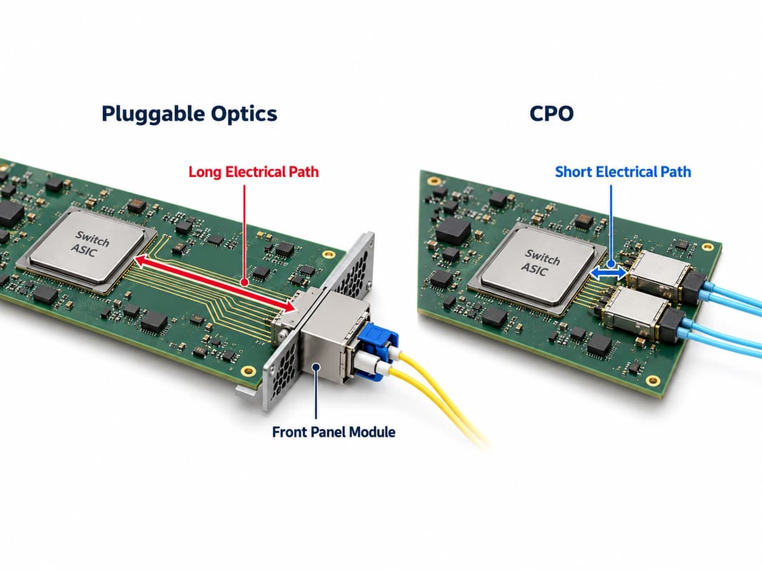
You may also like

AI Server PCB Design: Stackup, Signal Integrity and Power Delivery

August 13th, 2026

AI server PCB design must coordinate high-speed channels, dense accelerator routing, large transient currents, thermal limits, and manufacturable stackup details from the start. A board can pass ordinary design-rule checks and still fail if its material model, via structure, reference planes, power delivery network, and released fabrication data describe different electrical assumptions.

The practical goal is not to choose the highest layer count or the most expensive laminate. It is to convert the system architecture into a controlled board structure that can be simulated, fabricated, assembled, measured, and revised without losing traceability.

AI Server PCB Design on a high-density accelerator motherboard

What Is AI Server PCB Design?

AI server PCB design is the board-level engineering used for accelerator cards, server motherboards, backplanes, switch boards, power boards, and related high-performance computing hardware. It connects processors, accelerators, memory, storage, network interfaces, power conversion, management controllers, and mechanical interfaces within defined electrical and thermal margins.

The phrase should not be confused with AI-assisted PCB software. Here, “AI” describes the server workload and hardware architecture. The design challenge comes from dense interconnects, high aggregate bandwidth, fast current steps, large packages, and tight airflow or cold-plate constraints.

How Does an AI Server PCB Differ from a Standard Server Board?

An AI server PCB usually concentrates more high-speed lanes and higher power density around accelerators than a general-purpose server board. The exact difference depends on the platform, but the following design domains commonly become more tightly coupled.

Design Domain AI Server PCB Focus Release Evidence
High-speed links Loss, crosstalk, return paths, transitions, and connector channels Channel model, routing rules, and measured validation plan
Power delivery Low impedance across frequency, transient response, and current sharing PDN targets, plane geometry, capacitor strategy, and power test points
Density BGA escape, microvias, via-in-pad, and layer transitions Stackup, drill table, via structure, and fabrication feedback
Thermal and mechanical Package heat, copper distribution, stiffeners, connectors, and cooling interfaces Mechanical model, thermal assumptions, and assembly constraints

Which Board Architecture Should Be Defined First?

The board role must be defined before the stackup because a motherboard, accelerator card, backplane, and power board do not share the same routing or verification priorities. Start by mapping the interfaces, package transitions, connectors, board outline, cooling method, and power entry points.

  • Identify every high-speed interface and its end-to-end channel boundary.
  • Separate on-board routing from connector, cable, package, and mezzanine contributions.
  • Map voltage rails, expected current steps, conversion stages, and return paths.
  • Lock connector zones, keep-outs, fastener locations, stiffeners, and cooling interfaces.
  • Assign owners for SI, PI, thermal, mechanical, PCB, assembly, and validation decisions.

This architecture map prevents a local layout improvement from consuming margin needed elsewhere in the system.

How Should the AI Server PCB Stackup Be Planned?

The stackup should be derived from routing density, reference-plane continuity, impedance structures, power distribution, via transitions, total thickness, and fabricator constraints. There is no universal layer count for an AI server board.

Route critical signals next to continuous reference planes and minimize unnecessary reference changes. Power and ground planes should support the PDN strategy, while dielectric choices and finished copper thickness must match the values used in simulation. A proposed stackup is not controlled until the layout rules, impedance table, drill definitions, and fabrication drawing all describe the same build.

Cutaway of a multilayer AI server PCB stackup with through holes and microvias

For a focused introduction to a related commercial application, see our AI server PCB manufacturing overview.

Which Materials Support High-Speed AI Server Links?

Material selection should follow the channel loss budget, operating frequency range, stackup construction, copper profile, thermal exposure, and supply availability. A laminate name by itself is not an electrical model.

Record the source and test conditions for dielectric constant and dissipation factor. Then align those assumptions with resin content, glass style, finished dielectric thickness, copper roughness, solder mask, and the fabricator’s available constructions. Approving an equivalent material requires more than matching a nominal Dk or Df value; the proposed construction must also preserve impedance, loss, reliability, and manufacturability.

How Should Signal Integrity Be Controlled?

Signal integrity should be controlled as an end-to-end channel, not as isolated trace-width rules. Model the package escape, vias, reference changes, connectors, and routed transmission lines together wherever those transitions consume meaningful margin.

  • Define impedance by routing layer, structure, reference plane, and tolerance.
  • Budget insertion loss, return loss, crosstalk, skew, and discontinuities by interface.
  • Reduce avoidable via stubs and model backdrill or blind-via transitions.
  • Place return vias where a signal changes reference planes.
  • Preserve pair geometry through breakouts, bends, neck-downs, and connectors.
  • Plan coupons, test points, and correlation methods before fabrication release.

Our guides to stripline versus microstrip routing and eye diagram signal integrity explain two parts of this verification path.

Engineer measuring signal integrity on an AI server PCB with an oscilloscope eye diagram

How Should Power Integrity Be Designed?

Power integrity should keep every critical rail within its allowed voltage window during steady-state and transient operation. The work begins with target impedance and current-step assumptions, then connects regulator placement, plane geometry, decoupling, vias, and measurement access.

Place high-frequency decoupling close to the package power pins through short, low-inductance connections. Use appropriate plane areas and via arrays for current flow, but check the thermal and fabrication consequences of heavy copper concentration. Simulate the PDN over the relevant frequency range and reserve probe access for board-level correlation.

How Should Thermal and Mechanical Constraints Be Coordinated?

Thermal and mechanical decisions must be included before placement is frozen because cooling hardware, board stiffness, package warpage, and connector loading can change the electrical layout. A thermally attractive component location may be poor if it lengthens critical channels or blocks power entry.

  • Coordinate heatsinks, cold plates, airflow, mounting hardware, and keep-outs with placement.
  • Review copper balance, board thickness, panel support, and assembly thermal mass.
  • Protect press-fit zones, edge connectors, and large packages from excessive board flex.
  • Place temperature sensors and validation points where they measure meaningful conditions.
  • Define operating and qualification profiles before selecting materials and assembly cycles.

Which Via Structures Work for Accelerator Escape Routing?

The via structure should solve BGA escape and transition performance without creating an unnecessarily complex build. Through vias remain useful where density and channel performance allow them; blind, buried, and laser-drilled microvias are selected when routing density or stub control requires them.

For an AI accelerator PCB or GPU PCB design, review pad size, capture pad, antipad, aspect ratio, stacked or staggered construction, copper filling, planarization, sequential lamination, and inspection access together. Our microvia aspect ratio guide explains why geometry must be confirmed before release.

AI accelerator BGA escape routing with via-in-pad microvias and multilayer power planes

How Does AI Server PCBA Affect the Layout?

AI server PCBA requirements affect pad design, component spacing, thermal profiling, inspection access, rework strategy, and panel support. Dense BGA packages, heavy copper areas, large connectors, and mixed thermal masses make assembly feedback necessary before the board is finished.

Confirm the package land patterns and paste strategy against component data. Provide access for AOI, X-ray, boundary scan, programming, and functional test where applicable. If a critical BGA cannot be visually inspected, define the X-ray acceptance and process-control approach before production.

What Should Be Verified Before Prototype Release?

Prototype release should occur only after the electrical intent and manufacturing package agree. A file-count checklist is not enough; the review must find contradictions between files and assumptions.

  1. Confirm the board role, interface list, channel boundaries, power rails, and acceptance owners.
  2. Reconcile the stackup, impedance table, routing rules, material model, and total thickness.
  3. Compare every via depth pair and backdrill definition with the actual layer map.
  4. Review SI, PI, thermal, and mechanical assumptions against the released layout revision.
  5. Check Gerber, ODB++ or IPC-2581 data, drill files, fabrication notes, BOM, and placement data for revision consistency.
  6. Define coupons, measurements, test conditions, sample quantities, and pass/fail ownership.
  7. Record approved deviations and decide which changes require re-simulation or requalification.

Use the final URL for this AI server PCB design guide in project documentation so design, manufacturing, and validation teams reference the same release checklist.

FAQ About AI Server PCB Design

How many layers does an AI server PCB need?

There is no fixed layer count. The required stackup follows routing density, reference-plane needs, power distribution, board thickness, connector constraints, and the chosen via architecture. Select the layer count after preliminary placement, escape analysis, channel planning, and fabricator review.

Does every AI server PCB require HDI?

No. HDI is used when package escape, routing density, or transition performance cannot be achieved efficiently with conventional structures. Some support or power boards may not need microvias, while accelerator and dense compute boards often require more advanced interconnects.

Can standard FR-4 be used for AI server PCB design?

It may be suitable for slower support circuits or short channels, but critical high-speed links need a material decision based on the channel loss budget and construction. Do not approve a material from its generic family name alone.

Why is copper roughness important?

Copper surface profile contributes to conductor loss at high frequencies. The simulation model and fabrication specification should use compatible roughness assumptions, especially on long or margin-sensitive channels.

When is backdrilling required?

Backdrilling is considered when unused plated-through-hole stubs consume too much channel margin. The need and residual-stub target should come from transition modeling and must be translated into an unambiguous controlled-depth drill definition.

What is the most important PDN input?

The PDN needs credible rail tolerances, current demand, and transient assumptions. Without them, a target-impedance result may look precise but cannot prove that the processor or accelerator stays within its allowed voltage window.

How early should the PCB manufacturer review the stackup?

Review should start before routing rules and via structures are frozen. Early feedback can align available materials, finished dielectric thicknesses, copper weights, drill structures, and impedance geometries with the design model.

What test structures should be planned?

Plan structures that support the actual acceptance method, such as impedance coupons, loss or correlation structures, power test points, and assembly inspection access. Their design and location should be agreed before panelization.

What files should accompany an AI server PCB RFQ?

Provide the fabrication data, stackup, drill and backdrill definitions, impedance requirements, material assumptions, fabrication drawing, quantities, and revision. For assembly, add the BOM, centroid data, assembly drawings, test requirements, and any programming files.

How can prototype results be carried into mass production?

Keep the material construction, drill structure, process notes, test method, and acceptance evidence under revision control. If a production change alters an electrical or mechanical assumption, route it through the same owners who approved the prototype baseline.

How Can EBest Circuit Support Your AI Server PCB Project?

At EBest Circuit, we support PCB design, prototyping, fabrication, component sourcing, and PCB assembly from the same controlled data package. Our engineering review can help identify conflicts among the stackup, impedance requirements, drill structure, materials, assembly constraints, and released files before the order moves forward.

Send your Gerber or ODB++ data, stackup, drill files, impedance targets, BOM, quantities, and test requirements to sales@bestpcbs.com. Our engineering team can review the package and confirm the applicable manufacturing path for your project.

You may also like