As electronic products continue to shrink in size while increasing in functionality, engineers often need to integrate multiple circuit boards into a compact system. One common approach is PCB on PCB design, where one printed circuit board is stacked or connected directly on top of another.
This architecture allows designers to build modular systems, reduce footprint, and simplify product upgrades. However, designing a reliable PCB on PCB structure requires careful consideration of connectors, mechanical support, signal integrity, and assembly processes.
In this guide, we will explore how PCB stacking works, how engineers connect two PCBs together, and what design practices help ensure long-term reliability.
What Is PCB on PCB?
PCB on PCB refers to a structure where two or more printed circuit boards are connected directly together to form a layered electronic system. Each board usually performs a specific function. When combined, they operate as a complete device.
One board typically acts as the main board (motherboard). It contains the processor, power management, or key control circuits. The secondary board is often called a daughter board. This smaller board provides additional features such as sensors, wireless communication modules, or signal conversion circuits.
The connection between boards allows signals, power, and control data to travel between them. Instead of using long cables, engineers prefer direct board-to-board connections, which improve signal stability and reduce noise.

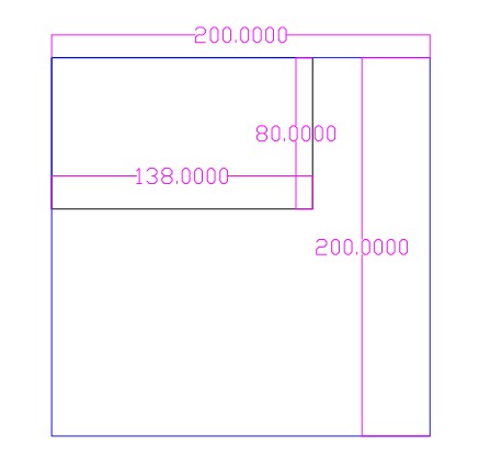
Typical PCB on PCB Structure
A typical PCB on PCB structure works through the following process:
- The primary board contains the core system circuits.
- Secondary boards add specialized functions.
- Electrical connectors or stacking structures link the boards.
- Signals transfer through dedicated connectors or pin interfaces.
This modular approach offers several advantages:
- Compact electronic design
- Easier upgrades or maintenance
- Flexible system expansion
- Improved manufacturing efficiency
Many advanced electronics rely on this architecture because it allows designers to isolate different functions while maintaining system integration.
Why Do Engineers Use PCB on PCB Designs?
Engineers often adopt PCB on PCB architectures when designing compact or modular electronic systems. The most important advantage is space optimization. By stacking boards vertically, designers can integrate more functionality within a limited enclosure. Other reasons include:
1. Modular system design
Different functions can be separated into individual boards. For example, RF circuits, power modules, and control logic can each be placed on dedicated PCBs.
2. Easier product upgrades
Manufacturers can update one module without redesigning the whole board.
3. Reduced design complexity
Complex circuits can be divided into manageable sections.
4. Improved manufacturing flexibility
Some modules can be produced or tested separately before final assembly.
Because of these benefits, PCB stacking design is widely used in telecommunications equipment, embedded systems, robotics, and IoT devices.

How to Connect Two PCBs Together?
When engineers search how to connect PCB to PCB, they usually refer to the physical and electrical methods used to link two circuit boards. Several techniques are commonly used in industry.
1. Board-to-Board Connectors
These connectors directly link two PCBs without cables. They are commonly used in compact electronic systems.
Advantages include:
- Reliable electrical connection
- Compact vertical stacking
- Easy assembly and maintenance
2. Pin Headers and Socket Connectors
Pin headers are a cost-effective solution for connecting PCBs. One board uses male pins while the other uses female sockets. They are widely used in development boards and industrial electronics.
3. Flexible Flat Cables (FFC)
Flexible cables allow PCBs to be connected while maintaining mechanical flexibility. This method is common in displays, laptops, and cameras.
4. Soldered Board Stacking
In some cases, boards are directly soldered together using metal spacers or solder joints. This approach is less common because it reduces serviceability.
Choosing the right method depends on factors such as space constraints, signal speed, mechanical strength, and cost.
What Is the Difference Between Stacked PCB and Daughter Board?
Many engineers confuse stacked PCB design with the daughter board architecture, but they are not exactly the same.
A daughter board is a secondary PCB that connects to a mainboard to extend functionality.
The main board, often called the motherboard, handles core system functions such as power management and data processing.
The daughter board usually provides specialized functions such as:
- communication modules
- sensor interfaces
- memory expansion
- power modules
In contrast, stacked PCBs describe the physical arrangement where boards are mounted vertically. A daughter board can be part of a stacked PCB system, but stacking can also occur in other configurations such as mezzanine structures.
How Do You Design a Reliable PCB on PCB Structure?
A reliable stacked PCB design requires careful planning. Electrical, mechanical, and thermal factors must work together. Engineers typically follow several design principles:
1. Ensure Stable Mechanical Alignment
Connectors must align perfectly during assembly. Misalignment can damage connector pins or reduce signal reliability. Designers often add mechanical guide posts or positioning holes to help assembly.
2. Control Signal Integrity
High-speed signals require controlled impedance routing. The connector structure must support stable signal paths.
Key factors include:
- Differential pair routing
- Controlled trace impedance
- Ground reference continuity
3. Provide Reliable Power Distribution
Power lines between stacked boards must support stable current flow. Designers often add multiple ground pins and power pins within connectors.
4. Manage Thermal Conditions
Components in stacked boards may generate heat. Proper spacing allows airflow and heat dissipation.
5. Consider Assembly Tolerance
Manufacturing tolerances influence connector placement. Engineers design with sufficient margin to avoid mechanical stress.
Following these design practices helps maintain reliable system operation throughout the product lifecycle.
What Are the Assembly Challenges for PCB on PCB Structures?
Although PCB stacking design offers many advantages, it also introduces several manufacturing challenges. The most common issues include:
1. Connector Alignment
Precise alignment is required to avoid connector damage during assembly.
2. Tolerance Control
Stacked structures must maintain tight mechanical tolerances to ensure proper board spacing.
3. SMT Assembly Sequence
When multiple boards are involved, the assembly process must follow a controlled sequence.
For example:
- Primary board SMT assembly
- Connector installation
- Secondary board mounting
4. Inspection Difficulty
Dense stacked structures can make inspection and rework more challenging.
Experienced PCB manufacturers typically address these issues through DFM analysis and optimized assembly processes.
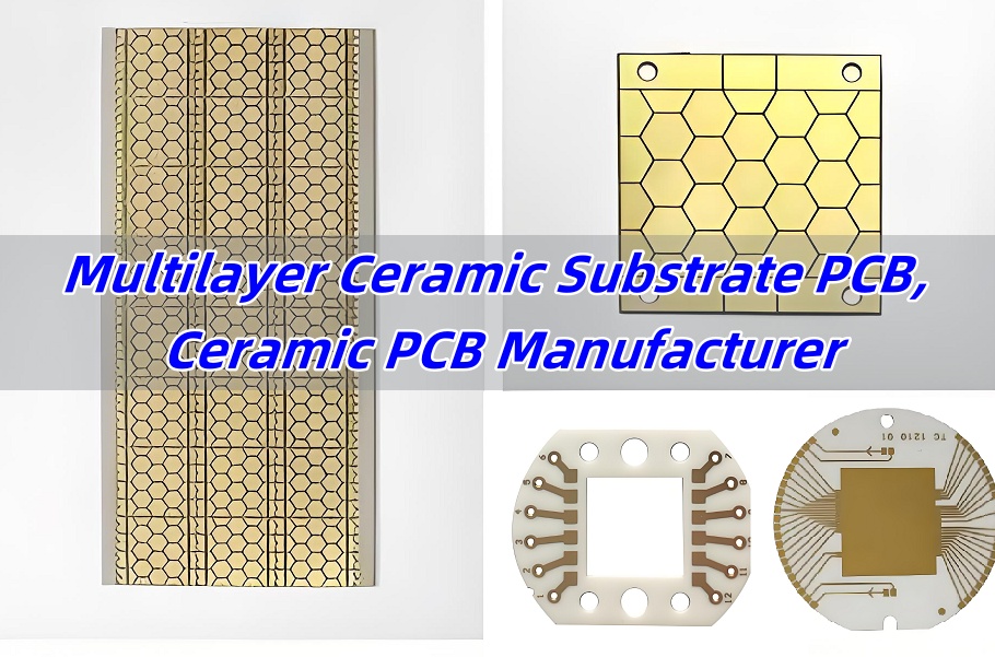
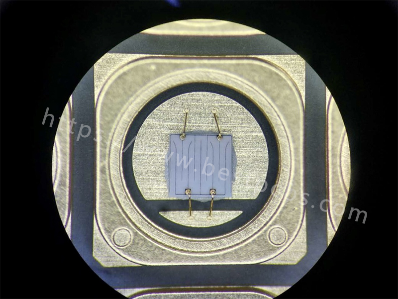
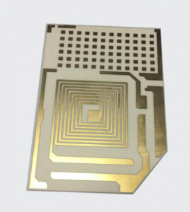
Can a Ceramic PCB Stacked on a FR4 PCB?
Yes, a ceramic PCB can be stacked on an FR4 PCB, but the design must account for several factors.
Ceramic PCBs such as Alumina (Al₂O₃) or Aluminum Nitride (AlN) have very different mechanical and thermal properties compared with FR4. Important considerations include:
- Thermal expansion mismatch
Ceramic materials have lower thermal expansion than FR4, which may create mechanical stress.
- Connector compatibility
The chosen board-to-board connector must support different board thicknesses.
- Thermal advantages
Ceramic PCBs provide excellent heat dissipation and are often used for power electronics or RF modules.
When properly designed, combining ceramic and FR4 boards can create highly efficient hybrid electronic systems.

Why Work With an Experienced PCB on PCB Assembly Manufacturer?
Designing and assembling stacked PCB systems requires expertise in both PCB fabrication and PCB assembly. At Best Technology (EBest Circuit), we specialize in complex PCB and PCBA projects, helping engineers bring advanced designs into production.
Our advantages include:
- 20 years of PCB and PCBA manufacturing experience
- Dedicated engineering support with DFM analysis
- PCB fabrication, component sourcing, and assembly in one place
- MES traceability system for quality control
- Rapid PCBA turnaround of about 1.5 weeks
Our engineering team works closely with customers to ensure that PCB on PCB designs meet performance, reliability, and manufacturability requirements.
For project inquiries, please contact: sales@bestpcbs.com
FAQ
What is PCB stacking?
PCB stacking refers to a design method where multiple circuit boards are arranged vertically and connected through board-to-board connectors or stacking interfaces.
This technique reduces product size and improves modular system architecture.
What connector is used for PCB-to-PCB connection?
Several connectors support PCB-to-PCB connections, including:
- Mezzanine connectors
- Board-to-board stacking connectors
- Edge card connectors
- Pin headers and sockets
The connector type depends on the electrical design and mechanical structure.
How do you stack PCBs safely?
Engineers stack PCBs safely by following several key practices:
- Use reliable board-to-board connectors.
- Maintain proper spacing between boards.
- Ensure strong mechanical support.
- Provide adequate airflow for thermal management.
These steps protect both electrical performance and mechanical durability.
Can stacked PCBs affect signal integrity?
Stacked boards can influence signal integrity if connectors introduce impedance mismatch or signal reflection.
Designers address this by:
- Using controlled impedance connectors
- Maintaining proper grounding paths
- Keeping high-speed traces short and symmetrical
With proper design, stacked PCBs maintain stable signal performance.
What industries use PCB stacking?
PCB stacking appears in many modern industries:
- Consumer electronics
- Automotive electronics
- Industrial automation
- Medical devices
- Robotics and IoT systems
These sectors benefit from compact system design and modular architecture.