PCB manufacturing PCB manufacturing
Home > Blog

solder paste printing

How Do You Choose an Aluminum Frame PCB Stencil?
Tuesday, September 15th, 2026

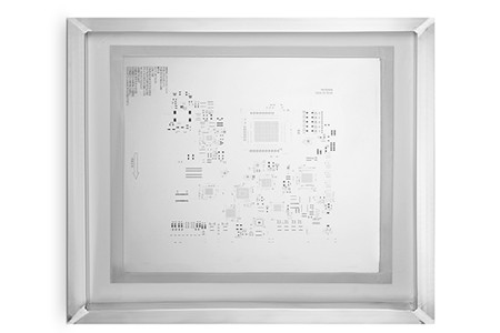
An aluminum frame PCB stencil holds a patterned metal foil under tension so solder paste can be printed onto PCB pads before component placement. The aluminum is the support frame, not normally the printing foil. At EBest Circuit (Best Technology), we supply custom SMT stencils and PCB assembly support. For your project, the useful starting points are printer compatibility, aperture geometry, foil thickness and the final panel layout.

Illustration of an aluminum frame PCB stencil with a mesh border and stainless steel foil

What Is an Aluminum Frame PCB Stencil?

A framed PCB stencil combines three working parts: a rigid frame, a tensioned mesh border and a thin metal foil containing openings that correspond to the solder-paste pattern. The squeegee moves paste across the foil; the openings control where paste reaches the board. After separation, the paste deposits remain on the pads.

The distinction between frame material and PCB stencil material matters when ordering. Aluminum provides a lightweight, rigid support. Stainless steel is commonly used for the PCB stencil foil because it can be fabricated with fine openings and withstand repeated printing and cleaning. A steel foil does not turn the finished circuit board into an aluminum PCB.

A PCB framed stencil is a complete mounted tool, whereas a stencil blank is an unpatterned starting material. If you need a working circuit board stencil, specify the aperture file and mounting arrangement, not just the frame dimensions.

Framed vs Frameless Stencil: Which Suits Your Production?

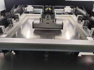
A permanently framed tool is useful for repeat builds on compatible equipment. A frameless foil can suit either a manual fixture or a reusable tensioning system, but those are different setups. Frameless does not automatically mean unsuitable for production.
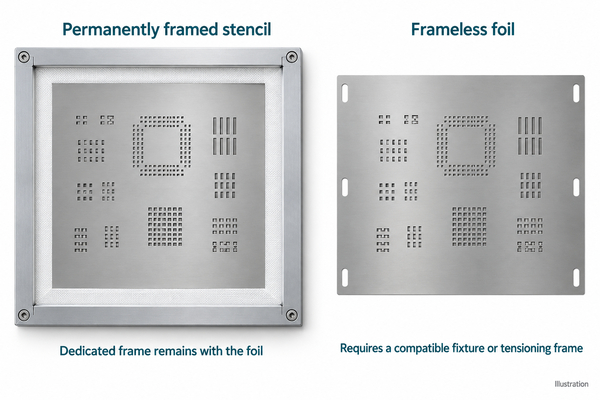
Illustration comparing a permanently framed stencil with a frameless foil requiring compatible mounting
Option Best fit What to check
Permanently framed stencil Recurring assemblies with a dedicated tool Printer fit, stored-frame space, mesh and bond condition
Frameless foil in a reusable frame Multiple designs sharing compatible tensioning hardware Foil mounting interface, tensioning procedure and changeover time
Unframed foil in a manual fixture Low-volume builds and development work Flat support, registration and repeatability of the fixture

For a frameless PCB stencil printer, confirm the foil attachment system before ordering. A foil made for one tensioning system may not fit another. Prototype SMT stencils should therefore be selected around the intended printing process, not around a fixed prototype-versus-production label.

What Frame Size Fits Your Stencil Printer?

There is no single PCB stencil standard size that fits every printer. The outer frame must fit the machine clamps, while the usable printing area must accommodate the complete panel and squeegee travel. Frame profile, thickness, mounting direction and underside-cleaning clearance also affect compatibility.
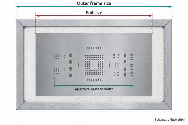
Schematic distinguishing outer frame size, foil size and aperture pattern width

An SMT stencil frame drawing should distinguish the outer frame size, foil size and aperture-pattern envelope. The actual printable area is further limited by bonding margins and the printer mechanism; it is not simply the entire foil. Send the printer model or approved mounting drawing instead of ordering a frame from PCB length and width alone.

A PCB stencil holder or PCB stencil jig must support registration without bending the foil or board. For our FR4 printed circuit boards, use the released panel drawing, including rails, orientation and fiducials, when preparing the stencil. Changing the panel after cutting can make an otherwise accurate stencil unusable.

How to Choose PCB Stencil Thickness?

Choose thickness from the paste-volume requirements of the component mix and the release behavior of the smallest openings. A thicker foil provides more theoretical paste volume for the same aperture, but also increases the wall area that the paste must release from. More thickness is not automatically better.

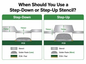
Our custom SMT stencil options cover a foil-thickness range of 0.10-0.60 mm across different stencil applications, subject to engineering review. This capability range is not a recommended thickness range for every fine-pitch SMT board. We also offer step-up and step-down stencil options where different areas need different deposit volumes.

For mixed fine-pitch ICs and larger terminals, evaluate a uniform foil first, then consider local thickness changes if the requirements conflict. Step locations need clearance from nearby apertures and suitable squeegee access. Component pitch alone is not enough to select PCB stencil thickness.

How Does SMT Stencil Aperture Design Affect Paste Release?

SMT stencil aperture design determines both deposit geometry and release conditions. For a rectangular opening with length L, width W and foil thickness t, area ratio is LW / [2t(L + W)]. Aspect ratio is W/t when W is the smaller opening dimension. These describe different geometric relationships.
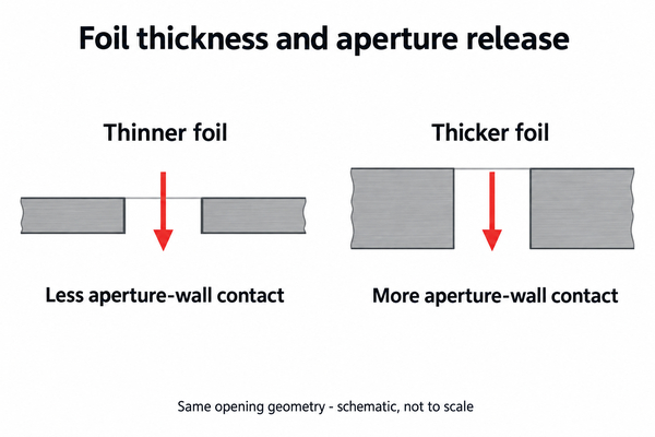
Schematic showing greater aperture-wall contact with thicker stencil foil for the same opening
Illustrative opening Foil thickness Area ratio Theoretical aperture volume
0.30 × 0.60 mm 0.10 mm 1.00 0.018 mm³
0.30 × 0.60 mm 0.15 mm 0.67 0.027 mm³

These calculated values illustrate geometry, not a guaranteed process window or measured deposit. Actual transfer depends on paste, aperture-wall condition, separation settings and board support. A PCB stencil thickness calculator cannot replace a print trial on the intended assembly.

For large thermal pads, multiple smaller windows may help distribute paste more appropriately than one large opening. For small pads, excessive aperture reduction can make release harder. PCB stencil design should use the component manufacturer’s land-pattern guidance, target deposit and assembly process together; a universal reduction percentage is not suitable for every footprint.

Which Fiducials and Panel Details Must Match?

PCB stencil fiducials let the printer align the foil pattern to the board. Their locations, optical contrast and marking method must suit the vision system. A fiducial is not necessarily an open hole: etching, filling or other marking arrangements depend on the printer and stencil specification.

For double-sided assemblies, identify top and bottom paste files explicitly and confirm viewing direction. Do not mirror a file merely because it is named bottom. The manufacturing output convention and assembly orientation must agree. When both sides share one foil, the printer’s working area, orientation and separation between patterns need approval.

Keep the PCB paste layer, panel drawing and assembly revision synchronized. The solder-mask layer is not a substitute for the paste layer: mask openings expose board features, while paste apertures define deposits for assembly.

How Is a Laser Cut PCB Stencil Made?

A laser cut PCB stencil is produced by cutting the approved aperture pattern into metal foil, applying the specified finishing operations and mounting the foil to its support system. In a permanently framed construction, the foil and mesh bond must maintain the required tension and flatness during use.

Our PCB stencil service includes laser-cut, etched, framed and unframed constructions, as well as electropolishing options. For a laser cut SMT stencil, electropolishing can improve aperture-wall condition, but it does not correct the wrong aperture geometry, foil thickness or panel file. The finishing requirement belongs in the order specification.

Before release, agree on the features that need verification: aperture dimensions and positions, foil thickness, image orientation, frame compatibility, bond condition and tension where specified. For fine-feature work, clarify the measurement method and acceptance criteria rather than assuming the word precision defines them.

How to Use a PCB Stencil?

The basic sequence is alignment, printing, controlled separation and deposit inspection. For a new framed tool, a short first-article print check is more useful than assuming that successful clamping proves process readiness.

  1. Confirm the stencil revision, print side and matching PCB panel.
  2. Support the board and align the apertures to the pads using the printer’s specified registration method.
  3. Apply compatible solder paste and use the established squeegee and separation settings for the assembly.
  4. Inspect deposit alignment, bridging, missing paste and consistency before placing components.
  5. Adjust the process or aperture design from the observed defect, rather than compensating for every problem with more pressure.

SMT solder paste stencils are printing tools, not reflow fixtures. The stencil is removed before placement and reflow. Through our PCB assembly services, we support SMT, through-hole and mixed assemblies; discuss stencil supply together with your assembly files when you need a coordinated PCB and PCBA order.

How Should Framed Stencils Be Cleaned and Stored?

Use a cleaning method compatible with the solder paste, foil, mesh and bonding adhesive. Residue inside an aperture can reduce the next deposit, while contamination beneath the foil can contribute to smearing. Follow the applicable cleaning-equipment and chemistry instructions, and protect personnel according to the relevant safety information.

Do not scrape fine openings with tools that can alter their geometry. After cleaning, check for blocked apertures, dents, corrosion, lifted bonding and mesh damage. A visibly clean foil is not automatically a flat, tensioned tool.

Store each tool by design, side and revision in a protected SMT stencil rack or equivalent support. Prevent contact with the active foil area. Reuse depends on condition and validated printing performance, not a universal number of print cycles. A replacement foil must also match the original mounting system.

What Affects the Price of a Framed PCB Stencil?

Price depends on frame size, foil specification, aperture complexity, finishing, step features, inspection requirements and delivery arrangements. A low tool price can be poor value if it requires a new holder, cannot fit the printer or has to be remade after a panel revision.

Compare quotations against the same drawing and scope. Ask whether the price includes the aluminum frame, patterned foil, mounting, specified finishing and inspection. For repeat orders, confirm whether an existing frame can be reused and whether that service is actually included.

For suitable stencil orders, we can provide turnaround as fast as one working day. Availability depends on the design, finishing and order review; production time is separate from transport time. Tell us the required arrival date so that the quotation can address both.

What Files Do We Need for Your Custom Stencil?

For a custom aluminum frame PCB stencil, send the released paste-layer data and final panel information first. We accept Gerber and supported PCB/CAD design files. A PDF can explain dimensions and notes, but a drawing alone may not contain the complete aperture geometry needed for manufacture.

Input Include
Design identity Part number, revision, top/bottom side and units
Aperture data Paste Gerber or supported design files, approved modifications and critical features
Panel and alignment Final panel drawing, rails, fiducials and print orientation
Printer interface Machine model, outer frame dimensions, frame profile and clamping requirements
Foil and finishing Requested thickness, step regions, surface treatment and inspection criteria
Order scope Quantity, stencil-only or PCB/PCBA supply, destination and required arrival date

If the thickness or aperture treatment is not yet defined, identify the fine-pitch devices and larger solder-volume features for review instead of guessing a specification. Send your aluminum frame PCB stencil requirements to sales@bestpcbs.com. Our team can discuss the stencil construction and manufacturing scope with you before quotation.


You may also like

Paste Volume Variation PCB: Causes and Printing Fixes
Friday, September 11th, 2026

For “paste volume variation PCB” problems, the right correction depends on whether deposits are consistently off target or changing unpredictably. A small aperture that always prints low may need a design change; deposits that deteriorate during a run may need cleaning or better paste handling. Raising pressure for both problems can leave the original cause unresolved.

EBest Circuit (Best Technology) combines PCB fabrication and assembly support with laser-cut, electropolished stencils and solder paste inspection. Smooth aperture walls support paste release, while SPI identifies uneven deposits before component placement. For help matching stencil and inspection requirements to your next assembly, contact sales@bestpcbs.com.

paste volume variation PCB

What Is Paste Volume Variation in PCB Assembly?

Paste volume variation is the difference between solder paste deposits that should perform consistently. It can occur between equivalent pads on one board, between repeated circuits in a panel, or at the same pad on successive boards.

Different component terminations often need different paste volumes. A connector tab and a small resistor pad should not be compared simply by their measured volume in mm³. Compare each deposit with its own target, then evaluate the spread within groups of similar apertures.

Location and timing help separate the causes. A problem that follows one aperture points toward that opening or its release conditions. A problem covering one panel region points toward local contact or support. A change after a pause points toward restart behavior. These patterns narrow the investigation before printer settings are changed.

How Is Solder Paste Volume Measured with SPI?

In 3D solder paste inspection, the system reconstructs the deposit surface and calculates volume above a reference plane. Volume combines height and footprint: a broad, shallow deposit can contain less paste than its top view suggests.

For a straight-walled rectangular aperture:

Theoretical aperture volume = length × width × stencil thickness

Transfer efficiency (%) = measured deposit volume ÷ theoretical aperture volume × 100

For example, a 0.40 × 0.25 mm aperture in a 0.10 mm stencil has a theoretical volume of 0.010 mm³. If SPI measures 0.009 mm³, transfer efficiency is 90%.

That percentage is meaningful only with its reference. An SPI program may use a specified nominal deposit volume rather than theoretical aperture volume. Keep the reference consistent when comparing results across boards or recipe revisions.

Before treating small differences as printer drift, repeat the measurement on the same deposit. If the reported volume changes appreciably without another print, resolve the measurement or reference issue first. Otherwise, adjusting the printer may compensate for inspection noise rather than improve deposition.

Why Can Average Paste Volume Hide Printing Problems?

High and low deposits can cancel each other in an average. The following hypothetical results all use the same nominal volume:

Set Five measured results Average
A 97%, 99%, 100%, 101%, 103% 100%
B 70%, 85%, 100%, 115%, 130% 100%

Set A spans six percentage points; Set B spans sixty. Both averages are on target, but they describe very different printing behavior. The example does not establish acceptance limits.

Keep two views of the data: the average shows centering, while the distribution shows consistency. A narrow cluster below target calls for correcting a persistent shortfall. A wide cluster calls for stabilizing the process before moving its center. Both volume and spread are used in solder paste performance evaluation.

Also keep critical locations visible. Averaging hundreds of larger deposits with a small fine-pitch group can conceal the group responsible for rejects. Compare similar aperture groups and retain the sequence of prints; a gradual decline is easier to recognize in order than in a combined histogram.

How Do Stencil Thickness and Aperture Design Affect Paste Release?

Stencil thickness sets theoretical capacity, while aperture geometry affects how readily that capacity transfers to the board. A thicker stencil holds more paste but also gives it more sidewall area to separate from.

Area ratio = aperture opening area ÷ aperture sidewall area

For a rectangular opening of length L, width W, and thickness t:

Area ratio = LW ÷ [2(L + W)t]

Using the earlier 0.40 × 0.25 mm opening, increasing thickness from 0.10 to 0.15 mm raises theoretical volume by 50%, but reduces area ratio from approximately 0.77 to 0.51. The larger cavity therefore does not guarantee a proportionally larger deposit. Area ratio and actual transfer efficiency describe different parts of the printing problem.

When small openings print inconsistently, consider reducing local thickness or revising opening geometry to improve release. Enlarging an opening is appropriate only where pad geometry and spacing allow the resulting deposit; it cannot be used indiscriminately around fine-pitch connections.

When larger terminations need more paste, a local step-up region may provide capacity without thickening the fine-feature area. Conversely, a step-down region can serve smaller openings. The step layout must still allow effective blade travel and stencil contact.

EBest Circuit supplies electropolished SMT stencils, including step-up and step-down options. These provide ways to address wall finish and local volume requirements within the stencil design, rather than relying entirely on printer adjustments.

How Do PCB Support and Squeegee Settings Affect Paste Volume?

Restore stable board-to-stencil contact first. An unsupported area can deflect during the print stroke, changing the seal around the apertures. Poor contact lets paste spread underneath the stencil instead of staying within the intended openings. Add or reposition suitable support beneath the affected area, correct clamping that lifts the board away from the stencil, and accommodate underside components in the tooling. This stabilizes the geometry on which pressure adjustments depend.

Use enough pressure to wipe the stencil clean. Too little pressure can leave paste on the top surface after the stroke. Increase it only until the blade produces a clean wipe under the chosen conditions. If excess force is needed, address blade wear, setup, or support rather than continuing to increase pressure.

Match speed to the paste’s filling behavior. The rolling paste bead drives material into the apertures. Changing speed changes both the available filling time and the paste’s response to shear. For a speed-sensitive paste that loses fill at higher speed, a lower setting can help. Other formulations perform well at higher speeds, so “slower is better” is not a universal rule.

Adjust separation for the difficult apertures. The board’s withdrawal from the stencil affects whether the deposit detaches cleanly or stretches and remains partly in the opening. Compare separation settings using the smallest troublesome group, while keeping the print stroke unchanged. Choose the setting that improves release and consistency, rather than automatically selecting the slowest separation.

paste volume variation PCB

How Can You Reduce Paste Volume Variation Across Repeated Prints?

A stable setup can still drift as residue builds up, paste sits idle, or material condition changes. Match the correction to the event that precedes the volume change.

Clear restricted apertures and remove underside residue. If particular deposits fall in volume as prints accumulate, examine those openings for retained material and clean them using the approved stencil-cleaning process. If paste spreads outside the intended footprint, remove underside contamination and restore contact. Shorten the cleaning interval when deterioration repeatedly starts before the next scheduled clean. More frequent cleaning will not repair poor support or an unsuitable aperture.

Prevent the cleaning cycle from introducing another variable. Use a cleaning agent compatible with the paste and avoid flooding the apertures. Complete the required drying stage before printing resumes. If the first print after cleaning is abnormal, correct the cleaning cycle rather than treating that print as ordinary production drift.

Control restart conditions after pauses. Apply the paste supplier’s recommended conditioning or kneading procedure where required, then inspect the restart print before placement. If stoppages are frequent, select a paste whose response-to-pause performance suits those interruptions. Changing the routine or material is more effective than repeatedly accepting a poor first print as inevitable.

Keep material handling consistent. Allow refrigerated paste to reach working temperature in its closed container before opening; opening it cold can introduce condensation. Track opening time and time on the stencil, follow the product’s working-life limits, and replace material that no longer meets those conditions. Do not assume all containers warm at the same rate.
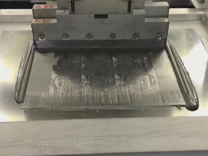
Confirm the improvement over the event that previously triggered the problem. A cleaning adjustment should remain effective through the revised interval; a restart correction should work after a representative pause. Use the same aperture groups and volume references before and after the change so the comparison reflects the process improvement.

What Soldering Defects Can Uneven Paste Deposits Cause?

The effect depends on whether a connection receives too little paste, too much, or an amount that is badly balanced against a neighboring connection.
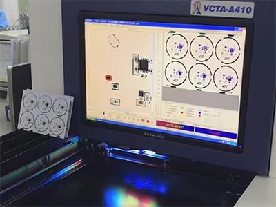
  • Insufficient solder or open connections: a severely underprinted location may lack enough solder to form the intended connection. Low deposits can also reduce contact margin where termination coplanarity or package warpage is already challenging.

  • Bridging: excess or spread-out paste can connect neighboring lands, creating a path for a solder bridge during reflow. Deposit position and spacing matter alongside volume; a misplaced deposit can cause trouble even when its volume is near target.
  • Tombstoning: unequal deposits on the two ends of a small chip component can contribute to an imbalance in wetting forces, allowing one end to lift.
  • BGA connection defects: uneven deposit heights can leave some balls with less contact than others. Warpage and oxidation can further interfere with coalescence, including in head-in-pillow failures.

These are possible outcomes, not a one-to-one defect code. Tombstoning also depends on thermal and wetting balance, while head-in-pillow involves the interaction between paste, solder balls, and package movement.

Trace the failed connection back to its SPI location. Repeated failures at the same low, high, or imbalanced deposits strengthen the case for a printing correction. If the deposits are consistent at those locations, investigate placement, solderability, and reflow instead of repeatedly changing the stencil.

paste volume variation PCB

FAQs About paste volume variation PCB

What paste volume tolerance should be used in SPI?

Set limits for the relevant aperture and component groups using the intended deposit volume and assembly results. A broad whole-board window can overlook sensitive locations; a tighter window is useful only when measurement repeatability supports it.

Can a deposit pass the volume limit and still be defective?

Yes. It may be offset, smeared, or connected to another deposit. Volume, position, and shape need to be considered together before components are placed.

Should the stencil be replaced if cleaning does not fix low volume?

Not automatically. Separate persistent geometry limitations or damage from paste-condition and printer-setup problems. Replacement makes sense when the opening or stencil condition is the confirmed limitation; an identical new stencil will not resolve an unsuitable design.

Is changing to a finer solder powder always the solution?

No. Powder size is one part of the paste formulation. A candidate paste must demonstrate suitable release through the actual openings, stability through production pauses, and acceptable reflow performance.

Can poor printing be corrected by changing the reflow profile?

A reflow adjustment cannot add missing solder or reposition a misplaced deposit. Correct unacceptable prints before placement, then use the qualified reflow process to form the joints.

For a new build or a repeat order with recurring print rejects, EBest Circuit can bring stencil supply and PCB assembly requirements into the same project discussion. Contact sales@bestpcbs.com to discuss whether your assembly needs a change in local paste volume, more consistent release, or closer inspection of specific component locations.

You may also like

Why Solder Paste became Dry and How to Solve This Problem
Thursday, August 18th, 2022

As a One-stop PCBA manufacturer, I believe most of manufacturers have faced a problem of solder paste became dry during SMT process, especially in hot summer, and there will be a large number of defects come out when solder paste was dry, such as poor printing, false solder, components be shifted, cold solder and so on, which will greatly decrease assembly efficiency and PCBA quality.

Do you know why the solder paste became dry?

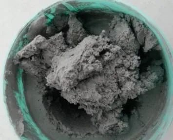
A serious dried solder paste
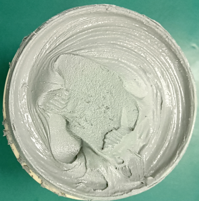
Good solder paste

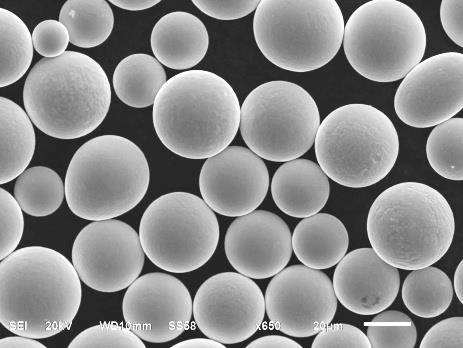
After checking and discussing with our SMT engineers, we found the root cause of solder paste be dry is corrosion, in below images you can see the detailed solder powder morphology of corrosion.

2-a Solder powder from good solder paste
2-b Solder powder from dried solder paste

In generally, the main reason of corrosion is thermodynamic instability of metal, that is metal and its alloy is in a high free energy status than other chemical compound (for example, oxide, hydroxide, salt or others), when this situation occurs, metal will transform to lower energy, which is called corrosion.

Metal corrosion is under the basis of the theory of electrochemical, and it’s required four main elements: anode, cathode, electrolyte and constitute current path.

Now let’s parse the mainly metals in solder paste — Sn, Ag, Cu (or other impurities), then under the action of flux medium, numerous galvanic cells with Sn as the cathode and Ag/Cu as the anode are formed, then below chemical reaction will be happened:

Cathode: Sn – 2e → Sn2+

Anode: O2 + H2O + 4e → 4OH

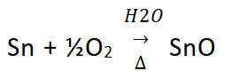
That is: Sn + H2O + ½O2 → Sn(OH)2

Sn(OH)2 decompose: Sn(OH)2 → SnO + H2O

Then chemical reaction of corrosion of solder powder under the moisture in the air can be described as:

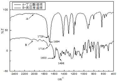
The following figure shows the infrared spectrum of succinic acid liquor before and after soaking the solder powder. It can be clearly seen that the soaked liquor contains carboxyl. Therefore, in the solder paste system, except the oxidation reaction of electrochemical corrosion, salinization chemical reaction will be happened too:

Infrared spectrum of Chemical reaction between succinic acid solution and solder powder succinic acid liquor

So now, do you know why solder paste will be dry? And why it is more seriously in hot summer with high temperature and humidity?

Yes, its root cause is not only high temperature in summer, also the humidity is so high (humidity is 70-85% in the summer of Shenzhen City), flux and solder powder will increase the adsorption of water molecules, and due to water is electrolyte of the galvanic cell reaction, it will aggravate the hydrolysis of flux, stimulate the activity of flux, then finally the reaction on the surface of the solder powder is aggravating, and the vicious cycle eventually changes the physical properties of the solder paste.

Then how to solve this problem?

  1. Warm up solder paste before using

Generally, in order to slow down the reaction of flux and solder powder, as well as extend the storage period, the solder paste needed to be stored in a refrigerator with 2-10oC degree. So before using, it is better to take out solder paste and put in standard room temperature for warming up first. A can of 500g solder paste need to be rewarmed at least 2 hours, to make sure its temperature is the same as rooms’. (Normally that period of warming up time is 4 hours in EBest Circuit (Best Technology).) Otherwise, insufficient warming up will cause the water vapor in the air to condense and enter the solder paste due to the temperature difference, and result in solder paste be dry finally.

  • Environment temperature and humidity

The best storage temp of solder paste is 2-10oC, but the recommended working environment temp is 20-25oC, relative humidity is 30%-60%. (There’re additional humidifiers in the workshop of EBest Circuit (Best Technology), to make sure suitable humidity in the dry season such as Winter and Spring, and of course the air conditioner in Summer time to decrease the humidity) Usually, the rate of chemical reaction will approximately double, as the temperature increases by 10℃, so the high temperature will increase the volatilization of the solvent in the solder paste and the reaction speed of flux with powder, so the solder paste is easily to be dry. Meanwhile, low temperature will affect the viscosity and expansion of solder paste, and then will cause the poor soldering. At the same time, high humidity will also greatly increase the water vapor entering the solder paste; However, low humidity also affects the volatilization rate of solvent in solder paste.

  • For those solder paste that became dried already, it is better to dilute with flux provided by manufacturer of solder paste.

In a word, when use and store solder paste, we should pay more attention to its temperature & humidity, to make sure high quality of SMT can be achieved. Pls contact EBest Circuit (Best Technology) if you have any questions or comments on solder paste, or SMT.

You may also like

The Application of AOI in Solder Paste Printing Inspection
Wednesday, December 12th, 2018

After we have talked about PCB inspection in last article, so today we move to the solder paste printing inspection. If you would like to learn something about PCB inspection, please click The Application of AOI in PCB Inspection.

AOI testing

AOI testing

Solder paste printing, the very beginning of SMT, is the root of most defects on the PCB. The defects occur in printing process is up to 60%-70%. Thus, if the defects can be avoided in this link, then the damage is able to save cost minimized. Therefore, most of printed circuit board manufacturers have already equipped with AOI testing in SMT production lines.

solder paste printing

solder paste printing

There are various of printing defects, but they can be generally divided into insufficient or excessive solder paste, the solder paste in the middle part of large pads scraped etc.. The reason why these defects are formed including unreasonable setting of printing machine parameter, low accuracy, improper selection for scraper and so on. However, it is effective to monitor the solder paste printing by AOI technology and analyze the number as well as types of defects, so that enhance the capability of printing.

EBest Circuit (Best Technology) is the premier expert in manufacture of PCB and PCBA. Our unique AOI testing technology and high quality products give you a competitive supply of printed circuit board and rigid-flex circuit board. To learn more, contact us at 0755-29091601 or check our website: https://www.bestpcbs.com/

You may also like