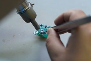
WLCSP assembly connects a chip-sized device to PCB pads through a fine-pitch array of solder balls. Those small connections save board space, but leave little room for uneven paste deposits, misplaced solder mask or rough handling. Reliable assembly depends on matching the footprint and process to the actual component—not simply selecting a recipe marked “0.4 mm pitch.”
EBest Circuit combines PCB fabrication, component sourcing and PCB assembly, allowing board construction and assembly requirements to be reviewed together. For a project containing WLCSP devices, contact sales@bestpcbs.com to discuss the component package and proposed PCB layout before the build.
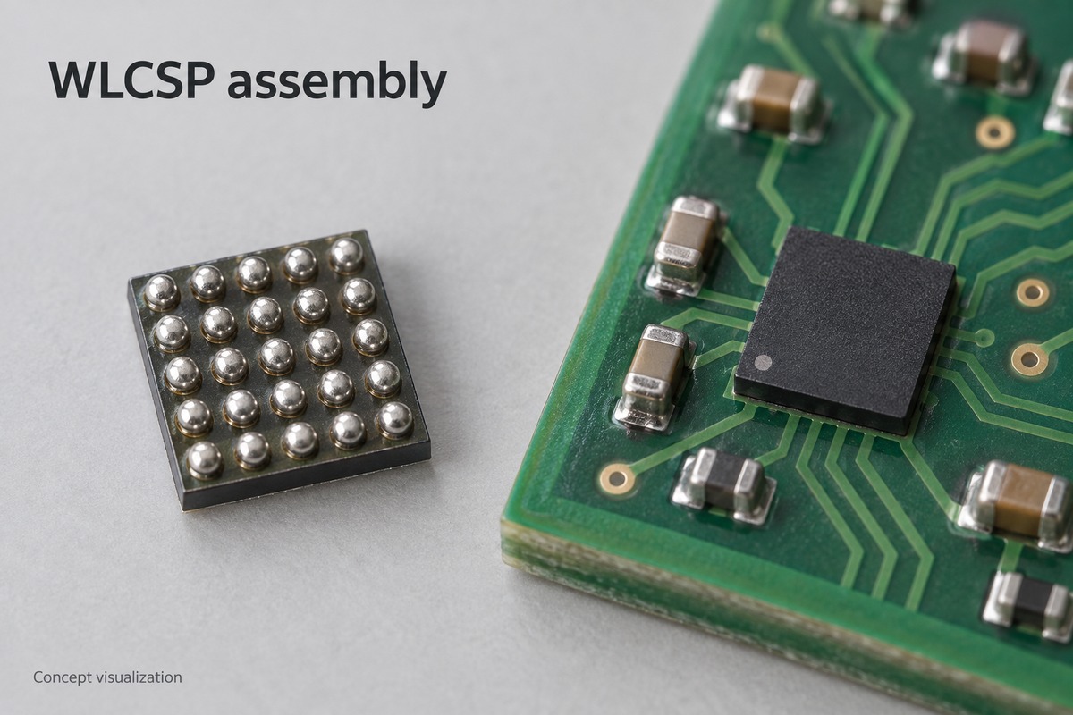
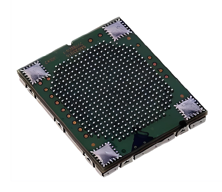
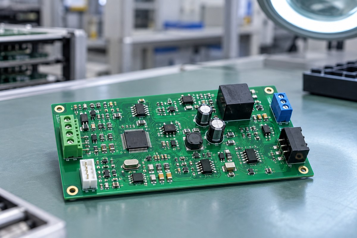
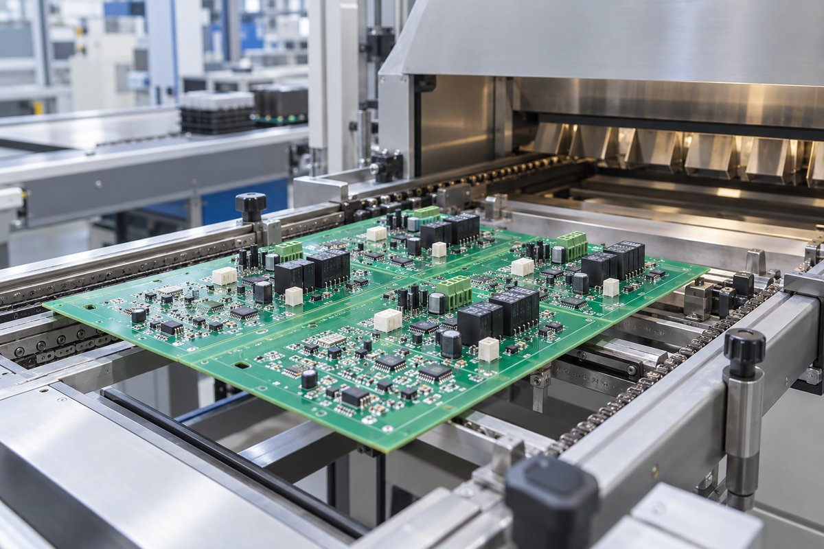
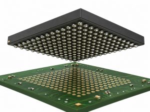
Concept visualization of a WLCSP solder-ball array and a board-mounted device.
What Is WLCSP Assembly on a PCB?
Board-level WLCSP assembly mounts an already packaged semiconductor device onto a circuit board. It is separate from the wafer-level processing that creates the package.
WLCSP stands for wafer-level chip-scale package. In a conventional fan-in WLCSP, the connections sit beneath the silicon die, within its footprint. There is no larger leadframe or laminate package substrate extending around it.
The board assembly still uses solder-paste printing, component placement and reflow. The difference is the small soldering geometry and exposed, mechanically sensitive package. Ball pitch describes spacing; it does not specify ball diameter, pad shape or handling limits.
How Do PCB Pads and Vias Affect WLCSP Solder Joints?
The exposed pad area controls where solder can wet, while the via structure can disturb the solder volume beneath a ball.
Pad construction
Exposed soldering surface
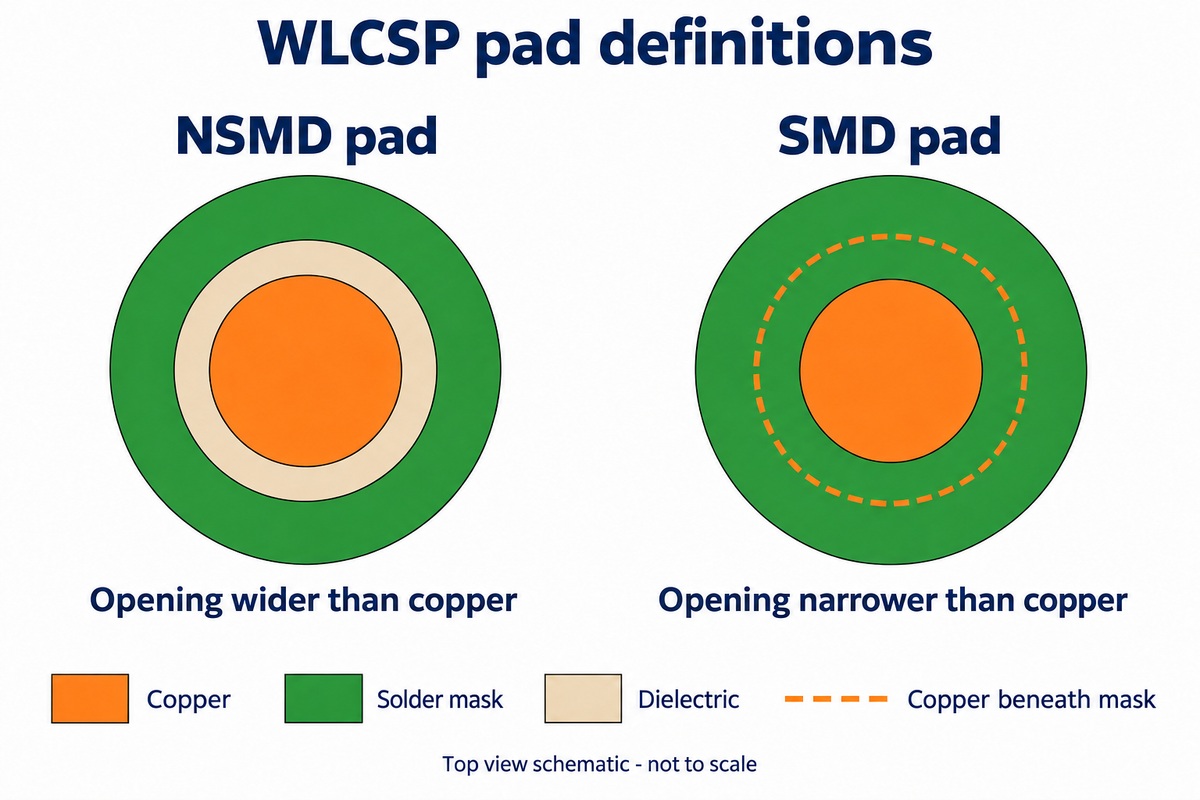
Non-solder-mask-defined (NSMD)
The mask opening is larger than the copper pad. Solder can wet the pad’s top and exposed edges.
Solder-mask-defined (SMD)
The mask opening is smaller than the copper pad. The opening defines the available soldering area.
Here, SMD describes the pad definition, not a surface-mount device. Neither construction makes a footprint interchangeable between different WLCSP parts. The component’s land-pattern recommendation determines the appropriate geometry.
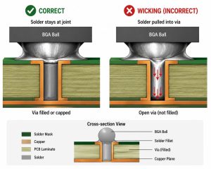
An unfilled via in a solder pad can trap air and contribute to voids or inconsistent joints. Where routing requires via-in-pad, a filled-via construction addresses this concern; the final pad surface still needs to meet the footprint requirements.
Mask registration also matters. A shifted opening can partly cover a pad that was correctly drawn in the CAD data.
NSMD and SMD differ in the relationship between the copper pad and solder-mask opening. Top-view schematic, not to scale.
How Does Stencil Design Control Solder Volume for WLCSP?
Stencil thickness and aperture geometry determine the paste available, but paste release determines how much actually reaches each pad.
A small aperture has relatively little opening area compared with its walls. Paste can remain inside instead of transferring cleanly to the PCB. Increasing stencil thickness adds potential volume while making release through that same small opening more difficult.
Aperture geometry governs the deposit footprint and release behavior.
Wall finish affects how readily paste separates from the stencil.
Paste particle size must suit the small opening and printing process.
A mixed-component board may need more paste at larger parts than at the WLCSP. A locally thinner stencil region can accommodate that difference, provided its transition works with nearby apertures. Post-print inspection reveals missing, uneven or displaced deposits before the package covers them.
How Are WLCSP Devices Placed and Reflowed?
Placement must align the ball array without damaging the die; reflow must then form joints within the component and paste process limits.
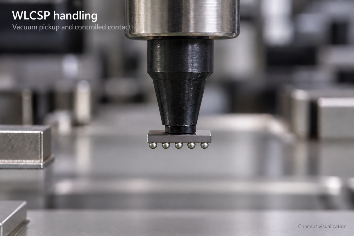
Vision alignment locates the device or its ball pattern. The pickup nozzle, placement height and applied force need to suit the package. A setup that handles a robust molded component successfully can still damage a small WLCSP.
Solder surface tension can help center the device during reflow, but that effect is not permission to accept arbitrary placement errors.
The thermal profile describes temperature at the assembly over time—not just the oven settings. Board loading, component location and neighboring parts affect heating. Profile measurements therefore need to represent the actual populated board.
A 260°C package qualification rating is not a universal reflow target. Peak temperature, time above liquidus and heating and cooling rates must satisfy the applicable component limits and solder-paste requirements together.
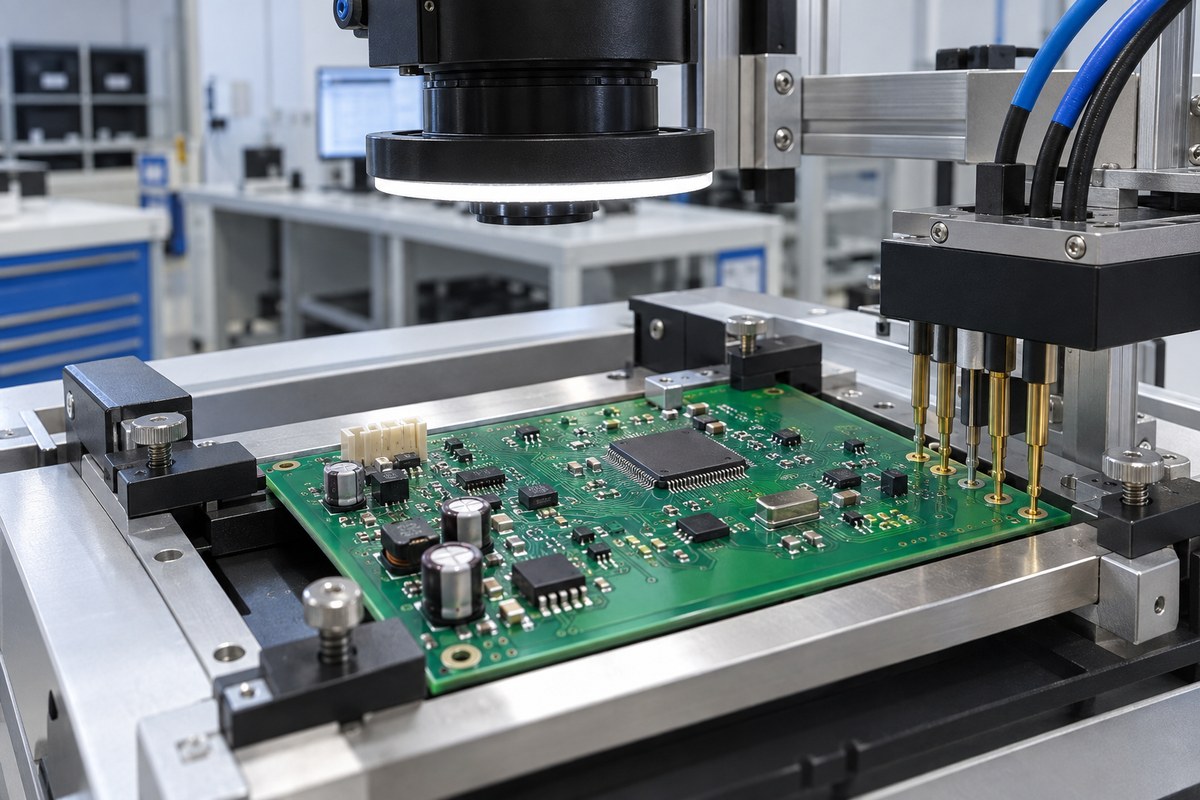
Concept visualization of vacuum pickup contacting the top of a WLCSP device.
How Are Hidden WLCSP Solder Joints Inspected?
The hidden array needs inspection beyond a top-down view of the component. Different methods answer different questions.
Method
What it can reveal
What it does not establish alone
Optical inspection
Visible damage, orientation and accessible joint edges
The condition of every joint beneath the die
X-ray inspection
Bridging, voiding and irregular solder distribution, subject to image quality and viewing angle
Electrical operation or lifetime under mechanical and thermal stress
Electrical testing
Opens, shorts or functional faults within the test coverage
The physical condition of every solder interface
A suspicious connection may need further analysis. Cross-sectioning can expose an internal interface, but destroys the examined area and is better suited to process investigation than routine inspection of saleable boards.
A board that powers on has passed that particular test; it has not automatically demonstrated solder-joint durability.
When Does WLCSP Assembly Need Underfill?
Underfill is not automatically required for WLCSP. Renesas recommends assembly without it for the packages covered by its implementation guide, which were qualified without underfill.
Underfill occupies the gap around the joints and changes how mechanical and thermal loads reach them. An application with demanding drop or bending conditions may justify evaluating reinforcement, but adding resin is not automatically a reliability improvement.
The material’s thermal expansion, stiffness, cure conditions and compatibility with residues all matter. Filling behavior and the fillet around the die also affect the result. A suitable material and process need validation on the intended assembly.
Underfill additionally changes repair options. A process chosen for reinforcement may make later component removal much harder.
Can WLCSP Components Be Reworked?
Replacement can be possible, but it needs a controlled process and an intact PCB footprint. Renesas discourages routine rework; Microchip describes a replacement process and advises against reusing removed devices in final assemblies.
Remove the device with controlled heating. Local heating and board preheating help release the soldered component without forcing it from the pads.
Restore the mounting site. Residual solder must be removed without lifting copper or damaging the solder mask.
Deposit paste and fit a new device. A miniature stencil and vision-assisted placement help reproduce the required soldering geometry.
Reflow and verify the replacement. The repaired location needs inspection and appropriate electrical testing.
A successful removal does not prove the board is ready for reuse. Damaged pads, underfill and the assembly’s previous heat exposure can limit repair.
For a WLCSP assembly project, EBest Circuit can review the PCB and PCBA requirements against your selected component. Email sales@bestpcbs.com with the part number and available board files to discuss the proposed build.
Single sided PCB assembly can reduce production complexity when every component fits on one assembly side and the soldering process remains straightforward. The real advantage is not simply having fewer populated surfaces. It is avoiding unnecessary second-side placement, extra board handling, and additional process steps while still meeting the product’s electrical, mechanical, thermal, and inspection requirements.
EBest Circuit manufactures bare PCBs and assembles customer-designed boards with SMT, through-hole, or mixed component populations. By reviewing the approved PCB data, BOM, component packages, polarity information, and test requirements together, we help customers move from prototype quantities to repeat production with fewer avoidable process changes. For a quotation or DFM review, contact sales@bestpcbs.com.
A single-sided PCBA keeps all component bodies accessible on one populated surface.
What Is Single Sided PCB Assembly?
Single sided PCB assembly means that all mounted components are placed on one side of the finished circuit board. This describes the component population, not necessarily the number of copper layers inside the PCB. A board can have one copper layer and components on one side, but a multilayer PCB can also use single-sided assembly when all packages are mounted on the same surface.
That distinction matters because “single sided” can refer to three different features:
A single sided PCB has one conductive copper layer.
Single sided assembly places all components on one side of the board.
Single-pass soldering describes a production route, but it does not automatically define the board’s copper-layer count or component layout.
Traditional single-layer boards often combine through-hole parts inserted from the component side with leads soldered on the copper side. An SMT design usually places both pads and components on the copper-patterned surface. Mixed technology can combine SMT and through-hole parts on one populated side, although the solder joints may be formed through different processes.
The practical benefit appears when the circuit is simple enough to remain accessible on one side. Fewer placement surfaces can simplify tooling, handling, visual inspection, repair, and process control. Once jumpers, awkward package orientations, thermal crowding, or excessive board area are needed to preserve that restriction, the single-sided format may no longer be the lower-cost solution.
How Are SMT and Through-Hole Components Placed on a Single Sided PCB?
SMT and through-hole components can share a single sided PCB, but their mounting and soldering paths are different. Surface-mount packages sit directly on pads. Through-hole parts pass through drilled holes, and their leads are soldered on the opposite surface. The placement plan must therefore consider component access, lead direction, solder contact, and the order of each operation.
For SMT-only assembly:solder paste is printed onto the pads, components are placed on the same surface, and the board passes through reflow. This is efficient for compact resistors, capacitors, ICs, and other packages that are suitable for automated placement.
For through-hole assembly: parts are inserted from the component side and soldered from the reverse side by wave soldering, selective soldering, or a controlled manual process. Connectors, transformers, relays, and mechanically loaded parts often use this method when their package or retention requirements make through-hole mounting appropriate.
For mixed assembly: SMT parts are usually placed and reflowed first. Through-hole parts are then inserted and soldered using a process compatible with the component bodies, spacing, and exposed SMT features. Pallets or selective soldering may be required when previously mounted parts must be protected from the solder wave.
Keeping all components on one side can make markings easier to read and service access more direct. However, the layout still needs adequate spacing around connectors, tall parts, polarized packages, test points, and soldering areas. A one-sided population only creates value if those features can be assembled without excessive manual correction or special handling.
How Does Single Sided PCB Assembly Move Through Production?
Single sided PCB assembly moves through production by matching the released board data and BOM to a controlled SMT, through-hole, or mixed-assembly route. A typical build follows this sequence:
A controlled process route can combine SMT and through-hole components on one assembly side.
Data and BOM review: Gerber or ODB++ data, drill files, drawings, centroid data, BOM details, component orientations, and revision identifiers are checked for agreement.
Bare-board fabrication and inspection: the PCB is built to the approved stackup, copper, solder-mask, surface-finish, outline, and hole requirements before assembly begins.
Material preparation: component identity, package, value, quantity, moisture sensitivity, polarity, and approved substitutions are controlled against the released BOM.
SMT processing where required: solder paste is printed, paste deposition is checked, components are placed, and the board is reflowed under an established thermal profile.
Through-hole processing where required: leads are inserted, formed when permitted, and soldered by the selected wave, selective, or manual method.
Cleaning, inspection, and testing: residues are managed according to the process specification, solder joints and component placement are inspected, and the agreed electrical tests are completed.
This route may be shorter than a two-sided assembly because the board does not require a second stencil print and placement cycle. It may also avoid the support, adhesive, or reflow considerations created by components on the underside. The actual saving depends on the component mix: a board dominated by manual through-hole work can still require substantial labor even though every part is on one side.
Stable repeat production depends on preserving the approved footprint geometry, solder volumes, component orientations, and process sequence. When a prototype uses hand-soldered substitutions or temporary jumpers, those exceptions should be resolved before the same board is treated as a production-ready single-sided assembly.
What Determines Single Sided PCB Assembly Cost?
Single sided PCB assembly cost is determined by the complete production route, not by component-side count alone. A one-sided population often costs less when it removes a second placement cycle, reduces fixtures and handling, and supports efficient panel processing. Those savings can disappear when the layout demands intensive manual insertion, unusual masking, selective soldering, rework, or a larger PCB.
The strongest cost drivers are:
Component count and package mix: automated SMT placement is usually more scalable than repeated manual insertion, lead forming, or hand soldering.
Board size and panel utilization: spreading a circuit over a larger one-sided board can reduce the number of units per panel and increase bare-board material cost.
Assembly sequence: mixed SMT and through-hole builds require more operations than SMT-only boards, even when all components occupy one side.
Tooling and soldering access: wave pallets, selective-solder fixtures, masking, or restricted nozzle access add setup and process time.
Inspection and test coverage: AOI, X-ray where applicable, in-circuit testing, functional testing, programming, and custom fixtures affect non-recurring and per-unit cost.
Volume and change frequency: prototypes absorb setup over few units, while stable repeat orders can distribute programming, stencil, tooling, and process-preparation costs more efficiently.
The lowest quoted board price is therefore not always the lowest finished PCBA cost. If a single-sided constraint increases board area, jumper count, hand work, or defect opportunities, a compact double-sided layout may produce a better total cost. Cost comparison should use the same quantity, test scope, sourcing responsibility, quality requirements, and delivery assumptions so that the two assembly options are evaluated on equal terms.
How Does Single Sided PCB Assembly Compare With Double Sided PCB Assembly?
Single sided PCB assembly usually offers a simpler production path, while double sided PCB assembly provides more placement area and routing freedom. The better option depends on whether the second populated surface removes more cost and risk than it adds.
Production factor
Single sided assembly
Double sided assembly
Component placement
All components occupy one surface
Components are placed on both surfaces
Typical process flow
One SMT placement side, with optional THT operations
Two placement sequences may be required
Board area
May need more area for the same component count
Can reduce footprint by using both surfaces
Handling and tooling
Usually simpler
Requires control of the first-side components during second-side processing
Compact, dense, interface-rich, or space-constrained products
A double-sided build does not automatically mean twice the assembly cost. Small passive components on the underside may allow a much smaller PCB, a shorter signal path, or a cleaner connector arrangement. Conversely, placing heavy or heat-sensitive parts on the second side can complicate reflow support and inspection.
The useful comparison is therefore process-specific. If all parts fit comfortably on one side with reliable solder access and acceptable board dimensions, single-sided assembly can keep production direct. If one-sided placement creates crowding, long routes, thermal concentration, too many jumpers, or difficult soldering, using both sides can make the finished PCBA easier to manufacture consistently.
Where Does Single Sided PCB Assembly Work Best—and Where Does It Fall Short?
Single sided PCB assembly works best in products with modest component density, uncomplicated interconnections, sufficient board area, and no strong need to minimize enclosure size. Common examples include simple power controls, indicator boards, appliance controls, relay boards, LED products, basic sensor interfaces, and low-complexity industrial electronics. The format is also useful when visible component identification and straightforward repair access matter.
Its limitations appear as the circuit becomes denser or more demanding. A one-sided component population can become restrictive when the product needs fine-pitch processors, large memory groups, many connectors, controlled-impedance interfaces, short high-current paths, extensive shielding, or concentrated thermal management. Forcing those functions onto one surface can enlarge the board or produce congested routing and uneven heat distribution.
Mechanical conditions matter as well. Tall components may conflict with the enclosure even if enough board area exists. Connectors may need fixed edge locations, displays or switches may have user-interface constraints, and heavy parts may require additional support. These factors can make a seemingly simple one-sided layout difficult to assemble or install.
The format is most successful when it follows the product’s real requirements rather than serving as an absolute design rule. Keeping one assembly side is worthwhile when it simplifies production without creating penalties elsewhere. When density, thermal performance, signal behavior, or enclosure limits become dominant, a double-sided or multilayer solution may deliver a more reliable and economical result.
How Are Single Sided PCB Assemblies Inspected and Tested?
Inspection and testing should verify both the general assembly quality and the features that are critical to the product’s function. Because components are concentrated on one side, visual access may be easier, but one-sided placement does not eliminate defects such as wrong parts, polarity errors, insufficient solder, bridging, lifted leads, contamination, or damaged through-hole barrels.
Optical inspection and electrical probing verify different aspects of the finished assembly.
The inspection route can include:
Incoming and bare-board checks for dimensions, finish, solder mask, markings, holes, and electrical continuity.
Solder-paste inspection for SMT builds where paste volume and alignment influence joint formation.
Automated optical inspection for component presence, orientation, polarity, placement, and visible solder conditions.
Visual inspection for through-hole fill, lead protrusion, solder bridges, flux residues, mechanical damage, and workmanship details not fully covered by AOI.
X-ray inspection when hidden joints or package geometry justify it; X-ray is not required merely because the assembly is single sided.
Electrical testing such as continuity, shorts testing, in-circuit testing, programming, or functional testing according to the agreed product requirements.
Inspection must match the technology on the board. A through-hole connector needs different acceptance evidence from a small SMT resistor, while a programmed controller requires more than a visual solder-joint check. Clear test limits, fixtures, firmware versions, and pass/fail conditions allow the finished units to be evaluated consistently across production lots.
FAQs About Single Sided PCB Assembly
Is a single sided PCB the same as single sided PCB assembly?
No. A single sided PCB has one conductive copper layer, while single sided PCB assembly means all mounted components occupy one side. A multilayer board can still use a one-sided component population.
Can SMT and through-hole parts be assembled on the same side?
Yes. SMT and through-hole parts can share one component side, but they normally require different placement and soldering operations. Their spacing and process order must allow each operation to be completed without damaging previously mounted parts.
Is single sided PCB assembly always cheaper?
No. It is often economical when it eliminates second-side processing without increasing board area or manual work. A double-sided assembly may cost less overall if it reduces PCB size, jumpers, routing difficulty, special tooling, or rework.
Can a multilayer PCB use single-sided component assembly?
Yes. Copper-layer count and component-side count are separate choices. A multilayer PCB may keep every component on one surface to simplify assembly or meet mechanical requirements.
What files are needed to quote a single sided PCB assembly?
A usable quotation package normally includes PCB fabrication data, a fabrication drawing or stackup requirements, the BOM, centroid or pick-and-place data for SMT parts, assembly drawings, polarity and revision information, and the required inspection, programming, and test scope.
Single sided PCB assembly is most valuable when one populated surface simplifies production without forcing extra board area, jumpers, or manual operations. EBest Circuit can review customer-released PCB and assembly data, manufacture the bare boards, source approved components, complete SMT and through-hole assembly, and perform agreed inspection and testing. To discuss a prototype or repeat-production build, contact sales@bestpcbs.com.
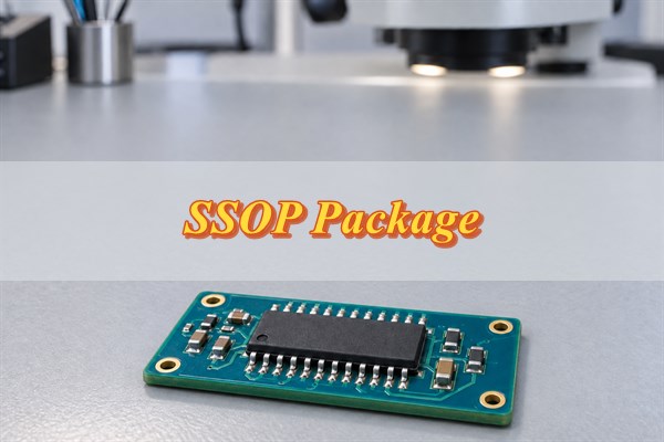
An SSOP package, or Shrink Small Outline Package, is a surface-mount IC package with gull-wing leads on two sides. It gives designers a compact, leaded package whose solder joints remain visible around the body.
SSOP is a package family, not one fixed mechanical outline. Two parts described as SSOP may use different body widths, lead spans, pitches, heights, and PCB land patterns, so the exact package code and manufacturer’s drawing must guide footprint design and assembly.
What Is SSOP Package?
SSOP stands for Shrink Small Outline Package, a compact surface-mount IC package with gull-wing leads arranged along two opposite sides. Compared with a standard SOIC of similar pin count, an SSOP generally uses a narrower body and finer lead spacing, reducing PCB area while keeping the solder joints exposed for optical inspection and rework.
SSOP describes a package family rather than one interchangeable outline. Confirm the exact manufacturer’s package code and drawing before choosing a PCB footprint because body width, lead pitch, overall span, height, and land-pattern requirements can differ. The practical tradeoff is greater board density with less assembly margin, so stencil design, placement accuracy, and solder-bridge control need closer attention.
What Are the Standard SSOP Package Dimensions?
There is no single set of SSOP package dimensions for every device. The same SSOP label covers multiple JEDEC outlines, body widths, heights, lead counts, and pitches. Use the package code on the exact component datasheet before selecting or creating a footprint.
The examples below from the NXP SSOP package index show how dimensions can vary within one manufacturer’s package family. The body column reports package length × body width × the height value listed by NXP, which may be nominal or maximum depending on the outline.
Package Example
Pitch
Body (mm)
SSOP16, SOT338-1
0.65 mm
6.2 × 5.3 × 2.0
SSOP20, SOT339-1
0.65 mm
7.2 × 5.3 × 2.0
SSOP24, SOT340-1
0.65 mm
8.2 × 5.3 × 2.0
SSOP28, SOT341-1
0.65 mm
10.2 × 5.3 × 2.0
SSOP16, SOT519-1
0.635 mm
4.9 × 3.9 × 1.73
SSOP48, SOT370-1
0.635 mm
15.9 × 7.5 × 2.8
These examples explain why SSOP-16 package dimensions or SSOP-20 package dimensions cannot be inferred from pin count alone. A 16-pin SSOP package can belong to a 5.3 mm-wide, 0.65 mm family or a 3.9 mm-wide, 0.635 mm family. Likewise, an SSOP-28 package should be checked by its package drawing rather than by an unqualified library name.
What Lead Pitch Does an SSOP Package Use?
A 0.65 mm lead pitch is common, but it is not universal. Official manufacturer package libraries also list 0.635 mm and 0.64 mm SSOP families, so the pitch must come from the exact package drawing or orderable-part datasheet.
Pitch is the center-to-center distance between adjacent leads. It controls pad spacing, solder-mask geometry, routing escape, stencil behavior, placement tolerance, and the optical resolution needed to detect bridges. Do not assume that a 0.65 mm footprint is compatible with a 0.635 mm package because the difference looks small; the offset accumulates across the lead row.
Confirm the pitch together with body width, lead count, overall lead span, lead width, lead length, and package height. Use that complete set of dimensions, not the pitch alone, to choose or build the PCB land pattern.
How Should You Design an SSOP PCB Footprint?
Build or select the footprint from the exact package code and its recommended land pattern. Component lead dimensions describe the part; they are not the same as the PCB pad dimensions needed to solder it.
Confirm the exact package code: Start with the manufacturer’s part number, package suffix, pin count, and drawing code. A library name such as “SSOP-20” is not specific enough on its own.
Check pitch and lead geometry: Read the specified pitch and the dimensional limits for lead width and length, body width and length, overall lead span, standoff, and coplanarity. A nominal body size alone does not show where every lead can land.
Use the recommended land pattern: Prefer the component manufacturer’s current recommendation when one is available. For example, TI’s DB0028A drawing shows 0.45 × 1.85 mm lands on 0.65 mm pitch for that specific 28-lead outline, not for every SSOP-28 package.
Check solder mask and paste openings: Confirm that the fabricator can hold the intended mask web and that stencil apertures suit the paste and assembly process. Excess paste can increase bridging, while too little paste can produce opens or weak joints.
Verify pin 1 and component orientation: Align the footprint marker, silkscreen, courtyard, centroid rotation, and assembly drawing. Leave enough access around both lead rows for optical inspection and rework.
Never assume that two SSOP devices with the same pin count can share a footprint. Compare the complete drawing and recommended land pattern before reusing a library part.
What Is the Difference Between SOIC and SSOP Packages?
SSOP is usually the better choice when board area is tight, while SOIC generally offers more assembly and rework margin. The table compares the points that most often affect package selection; exact dimensions and performance still depend on the orderable device and its package drawing.
What Users Care About
SOIC
SSOP
PCB area
Usually needs more board area for a similar lead count
Usually uses less board area for a similar lead count
Common lead pitch
Often 1.27 mm
Often 0.65, 0.635, or 0.64 mm
Assembly margin
Wider lead spacing gives more print and placement margin
Tighter spacing needs closer stencil, placement, and reflow control
Prototyping and hand soldering
Generally easier to place and solder manually
Feasible with suitable tools, magnification, and operator control
Inspection and rework
Exposed leads are easier to see and access
Exposed leads remain visible, but tighter spacing makes bridges and rework more demanding
Footprint compatibility
Not interchangeable with SSOP without checking the exact drawing and land pattern
Needs its own checked land pattern rather than an assumed SOIC footprint
SOIC is often easier to prototype, inspect, and rework when board area is available. SSOP is useful when density matters and the assembly process can control the finer pitch. Neither is a drop-in substitute for the other, even when the pin count and electrical function appear to match. The SOIC package guide provides additional SOIC-specific detail.
What Is the Difference Between SSOP and TSSOP Packages?
TSSOP is a thinner small-outline package family and is often more compact than a comparable SSOP, but the names alone do not prove footprint compatibility. In TI’s 20-pin package comparison, the DB SSOP has a 2.00 mm maximum height, while the PW TSSOP has a 1.20 mm maximum and occupies less footprint area. That example illustrates the family difference; it does not define every SSOP or TSSOP.
Pitch is not a reliable shortcut because both families contain multiple outlines. NXP listings, for example, include TSSOP packages at 0.65 mm and 0.5 mm pitch, while its SSOP listings include 0.65 mm and 0.635 mm examples. Before changing packages, compare pitch, body width and length, lead span, lead dimensions, height, pinout, and the recommended land pattern from the exact device drawings.
The same pin count or device family does not make an SSOP and TSSOP mechanically interchangeable. Treat a package change as a PCB footprint check, not as a name-based substitution.
Where Are SSOP Packages Commonly Used?
SSOP packages are common where a dual-row leaded IC must fit into limited board space while keeping its joints optically accessible. The package appears across many device classes; it is not tied to a single circuit function.
Logic and I/O: Buffers, latches, bus-interface devices, and I/O expanders are often offered in this compact leaded format.
Data conversion: ADCs, DACs, and mixed-signal ICs may use SSOP when the layout needs moderate pin density and visible leads.
Interfaces and communications: Transceivers, line drivers, and serial-interface devices are common candidates when routing space is limited but optical inspection still matters.
Analog and control: Op-amps, sensor interfaces, controllers, and clock devices are available in SSOP options when their pin count and thermal needs fit the outline.
Compact equipment: Industrial controls, consumer electronics, audio/video products, and communication hardware use SSOP when the smaller mounting area justifies the finer-pitch assembly process.
In practice, the exact device and mechanical outline should drive the decision. An application label by itself is not a reason to choose SSOP.
What Should You Consider When Selecting an SSOP Package?
Select the electrical device first, then verify that its exact SSOP option fits the board, assembly process, inspection plan, and supply strategy. Package size cannot compensate for an incorrect function, rating, or lifecycle choice.
Does the IC meet the electrical requirement? Confirm function, pinout, ratings, speed, accuracy, interfaces, temperature range, and any thermal limits for the real board conditions.
Does the exact outline fit the available PCB space? Check the package suffix, lead count, body size, lead span, height, courtyard, and routing access rather than comparing body width alone.
Can the PCB and SMT process handle the pitch? Match the pad, mask, stencil, placement, and reflow requirements to the fabricator and assembler’s capabilities.
Can the package be inspected and reworked? Allow optical access to both lead rows and enough surrounding space for the planned inspection and rework tools.
Will the exact package remain available? Check the component’s lifecycle, authorized supply options, and qualified alternatives early enough to avoid a late footprint change.
How Is an SSOP Package Soldered to a PCB?
Production SSOP assembly normally uses solder-paste printing, pick-and-place, controlled reflow, and inspection. Fine lead spacing makes print volume and lead-to-pad alignment more sensitive than they are for a wider-pitch package, but there is no universal SSOP temperature profile.
Print the solder paste: Align the stencil apertures with the pads and control deposit volume. Too much paste raises bridge risk; missing or incomplete deposits raise open-joint risk.
Place the component: Match pin 1 and align both lead rows with their pads. A placement offset can push one row toward bridging while leaving too little overlap on the other.
Reflow the assembly: Set the profile from the solder alloy and paste guidance, PCB thermal mass, and the component’s temperature limit. Board construction and nearby components change heating behavior, so a package name cannot supply one universal profile.
Inspect the joints: After reflow, check the exposed gull-wing leads for bridging, opens, misalignment, lifted leads, and poor wetting, then use electrical testing where product risk and test access justify it.
Footprint dimensions, package and board tolerances, placement accuracy, flatness, solder paste, and stencil behavior work together. A correct package drawing cannot compensate for the wrong land pattern or a shifted paste print.
What Assembly Problems Can Occur With SSOP Packages?
The most common SSOP assembly problems are bridges, opens, misalignment, lifted leads, poor wetting, and orientation errors. Start with what is visible, then check the process condition most likely to have produced it.
Observation
Likely Cause
First Check
Solder bridge
Excess or shifted paste, placement offset, pad or mask mismatch
Paste deposits, stencil apertures, placement image, and pad spacing
Open or low-solder joint
Missing paste, poor transfer, bent lead, coplanarity error, or weak wetting
Paste deposit, lead plane, pad finish, profile, and visible wetting
Component skew
Unequal deposits, placement error, or asymmetric reflow forces
Pad symmetry, deposit balance, and pre-reflow placement
Lifted lead
Lead damage, poor coplanarity, handling stress, or pad-height variation
Incoming lead condition, seating plane, board flatness, and local joint gap
Poor wetting
Oxidation, contamination, unsuitable profile, or expired/incorrect material
Lead and pad finish, paste condition, cleanliness, and reflow profile
Wrong orientation
Ambiguous marking or inconsistent library, CPL, feeder, and drawing data
Pin 1 on the part, footprint, placement data, and AOI model
Do not repair the symptom before confirming the cause. Removing a bridge may restore continuity on one board, but a shifted stencil or incorrect footprint can repeat the same defect across the lot.
How Should SSOP Solder Joints Be Inspected?
Inspect SSOP joints with visual or automated optical methods first because the gull-wing leads and fillets are exposed. Judge the joints against the applicable product requirement and assembly standard rather than a generic online photograph.
Confirm identity and orientation: Verify the part marking, package suffix, pin 1, polarity where applicable, and seating position before judging individual joints.
Inspect the lead rows: Check lead-to-pad alignment, unintended connections, insufficient solder, lifted or damaged leads, visible wetting, and consistent fillet formation at the toe and heel regions that can be seen.
Use AOI for repeatable coverage: Program the correct package geometry and joint criteria. AOI can compare every visible lead quickly, but lighting, library setup, board contrast, and obstructions affect its results.
Apply X-ray only when justified: X-ray is not automatically required for an ordinary exposed-lead SSOP joint. Use it when a hidden feature, overlapping structure, adjacent bottom-terminated device, or failure investigation cannot be resolved optically.
Add electrical testing where needed: Continuity, shorts, in-circuit, or functional testing can reveal failures that appearance alone cannot prove. Electrical testing complements solder-joint inspection; it does not replace it.
IPC-A-610 is widely used for electronic-assembly acceptance, but the applicable revision and class must come from the product or customer requirement. Do not infer pass limits from a photograph.
FAQs About SSOP Packaging
Q1: What do codes such as DB and DBQ mean on an SSOP listing?
A1: They are manufacturer-specific package designators, not interchangeable names for one outline. For example, two SSOP codes can indicate different body widths or lead pitches. Match the code on the orderable part number to the drawing in the same datasheet.
Q2: Can an SSOP IC plug directly into a solderless breadboard?
A2: No. SSOP is a surface-mount package, and its fine lead spacing does not match a standard 2.54 mm breadboard grid. For prototyping, solder the IC to a suitable SSOP-to-DIP adapter or use a purpose-built carrier board.
Q3: What should you check before buying an SSOP-to-DIP adapter?
A3: Match the adapter to the exact pin count, lead pitch, body width, lead span, pad layout, and pin 1 orientation. A board labeled only “SSOP-16” may not fit every 16-lead SSOP outline.
Q4: Does the SSOP name guarantee RoHS compliance?
A4: No. SSOP describes the package family, not the terminal finish or environmental status. Check the exact orderable part number, material declaration, and applicable compliance documentation.
Q5: How should moisture-sensitive SSOP parts be stored before reflow?
A5: Follow the moisture-sensitivity label and the component manufacturer’s handling instructions. Keep unopened parts in their specified moisture-barrier packaging. After opening the bag, observe the stated floor life and use controlled dry storage or baking only when the product instructions and applicable J-STD-033 requirements call for it.
Conclusion
The safest SSOP design starts with the exact orderable part, not a generic library name. Before PCB layout, confirm its pitch, body dimensions, lead geometry, package code, and recommended land pattern. That work gives printing, placement, soldering, and inspection a sound starting point.
If your PCB uses SSOP or another fine-pitch SMT package, send the part number, datasheet, PCB files, BOM, quantity, and assembly requirements to sales@bestpcbs.com for review and quotation.
A head-in-pillow defect occurs when a BGA solder ball and the printed solder paste fail to join properly during reflow. The two solder masses may touch, allowing the board to pass an electrical test, while the joint remains mechanically weak. This makes HIP especially troublesome in assemblies that work initially but develop intermittent connections during handling, temperature changes, or service.
EBest Circuit (Best Technology) supports BGA assembly with solder paste inspection, reflow soldering, and X-ray inspection. These capabilities help connect hidden solder-joint problems with the printing and assembly processes that influence them. For a BGA build affected by recurring soldering defects, contact sales@bestpcbs.com to discuss the assembly process and inspection approach.
Illustration of a head-in-pillow joint: the solder ball contacts the reflowed solder without forming a continuous metallurgical joint.
What Is a Head-in-Pillow Defect?
A head-in-pillow defect is an incompletely joined interface between the component's solder ball and the reflowed solder paste on the PCB. The paste may have wetted the copper land correctly, yet failed to merge with the ball above it. In a section through the joint, the ball can resemble a head resting on a pillow of solder.
Physical contact does not establish a sound solder joint. A reliable connection requires the solder surfaces to wet and coalesce. If an oxide film or other wetting barrier remains between them, the contact can conduct electricity without providing the strength expected from a properly formed joint.
The resulting failure may be an immediate open circuit or an intermittent connection. Temperature changes or mechanical movement can disturb that contact and expose the weakness. However, these symptoms alone do not identify HIP: cracked joints, damaged pads, and other BGA defects can produce similar behavior.
What Causes a Head in Pillow Defect During Reflow?
HIP develops when the solder ball and paste fail to maintain or recover the contact and wetting conditions needed to merge. Dynamic warpage is one important trigger, but oxidation, contamination, paste behavior, and flux activity also influence the outcome.
A typical warpage-related sequence is:
Initial contact: Placement brings the BGA balls into contact with the printed paste deposits.
Temporary separation: As the assembly heats, the package or PCB changes shape. Some balls lift away from their deposits.
Separate reflow and oxidation: The paste reflows on the land while the separated surfaces remain exposed. Oxide films can interfere with subsequent wetting.
Incomplete reunion: The package moves back toward the board, but renewed contact does not produce full coalescence if the interface is no longer wettable or the solder has solidified.
This explains why a package that appears flat after cooling can still contain defective joints. Its final shape does not reveal how it moved while the solder was forming.
Warpage is not the only route to HIP. Oxidized or contaminated solder balls can resist wetting even when their initial contact with the paste is adequate. Flux must remove surface oxides and protect the interface during the useful soldering period; the presence of flux residue after reflow does not prove that sufficient activity remained when the ball and paste needed to join.
Defects concentrated near BGA corners can suggest package movement or temperature differences. That pattern is a diagnostic clue, not proof of a single cause.
How Does a Head on Pillow Defect Differ from a Non-Wet Open?
Head on pillow, also called HoP, describes the same general defect family as head-in-pillow. The important distinction from a BGA non-wet open is where the connection fails to form.
Feature
Head-in-pillow / head on pillow
BGA non-wet open
Main failed interface
Between the solder ball and reflowed paste
Between the solder and PCB land
Typical solder distribution
Separate solder masses remain on the component and board sides
Paste can join the component ball and pull away from the land
Main diagnostic question
Did the ball and paste coalesce?
Did the solder wet the PCB land?
In the non-wet-open mechanism described here, solder can accumulate on the component side while the PCB land remains unwetted. HIP can leave solder attached to the land, with the defective interface above it.
Both conditions may produce an open or unstable electrical connection, but they direct the investigation toward different interfaces. A dark line, unusual ball shape, or failed continuity test cannot establish that distinction by itself. Examination of the affected joint must locate the actual separation or wetting failure.
Why Can a Head-in-Pillow Defect Escape Inspection?
HIP can escape inspection because the failed interface is hidden and may still make electrical contact. Different inspection methods reveal different parts of that problem.
Visual inspection and AOI have limited access. Most BGA joints sit beneath the package. AOI can identify placement errors and visible assembly defects, but it cannot establish the integrity of every hidden ball-to-paste interface.
Electrical testing captures the connection under the test conditions. A weak interface may touch well enough to pass continuity or functional testing. If the contact changes with temperature or movement later, the failure appears after the test has finished. Passing once therefore does not demonstrate that the solder masses have formed a reliable joint.
X-ray images require careful interpretation. A top-down image projects the joint through its thickness, so two touching but incompletely joined solder masses can overlap in the image. Oblique views or suitable three-dimensional imaging may reveal separation or unusual joint geometry more clearly. However, a narrow waist or suspicious outline is not, by itself, proof of HIP; joint shape can also create misleading indications.
When electrical symptoms and X-ray findings disagree, further failure analysis may be needed. Cross-sectioning or a controlled dye-and-pry investigation can provide additional evidence, although these methods are destructive and depend on preparation and interpretation. Such analysis is most useful when it targets the suspected location and is correlated with the original failure.
Inspection can identify suspect joints and support diagnosis. Preventing their formation still depends on controlling the assembly process.
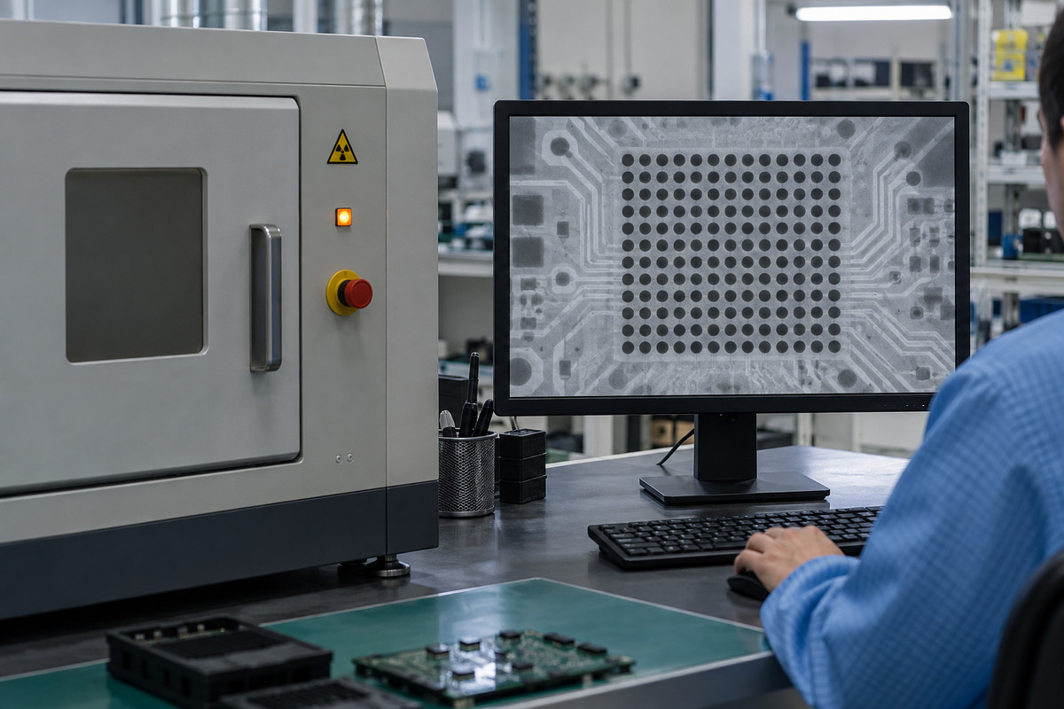
Illustrative BGA X-ray inspection scene. A two-dimensional projection alone may not resolve an unfused head-in-pillow interface.
How Do Solder Paste and Stencil Printing Affect HIP Risk?
Solder paste affects HIP through both contact geometry and wetting behavior. The printed deposit must reach the ball consistently, while the flux must remain effective during joint formation.
A low or uneven deposit can leave less contact margin when a package moves during reflow. Deposit height matters alongside volume: paste that spreads or slumps can contain solder but provide less vertical contact with the ball. Printing offset can also reduce the contact area between the ball and its intended deposit.
SPI helps reveal insufficient deposits, height variation, and printing misalignment before placement. Comparing the affected BGA locations with their print measurements can show whether the defect follows a printing problem. Consistent deposits at failing locations, however, leave package movement and wetting behavior as important possibilities.
Increasing stencil aperture size is not a universal correction. Additional paste may improve contact in a particular process, but too much can introduce bridging or alter joint geometry. The useful adjustment is one that improves deposit consistency and contact without creating another defect.
Flux chemistry also matters. Paste behavior during heating, oxide removal, and protection against further oxidation influence whether separated surfaces can join again. A paste that prints well at room temperature may still need evaluation under the actual BGA reflow conditions. HIP reduction therefore requires both a suitable material and a repeatable printing process.
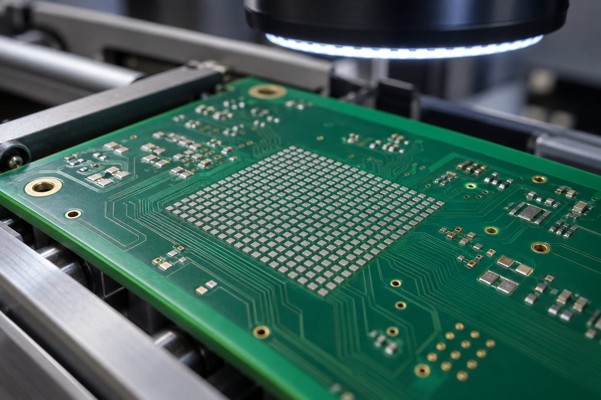
Illustrative inspection scene showing solder paste deposits on a BGA land pattern before component placement.
Can a Hotter Reflow Profile Eliminate HIP?
No. A hotter profile can help when inadequate heating is the problem, but it can also increase warpage, oxidation, or flux depletion. Temperature alone cannot ensure that the ball and paste remain in contact and wet each other.
The relevant temperature is the one experienced by the assembly, not simply the oven setpoint. A large BGA and the surrounding PCB can heat unevenly. Raising the oven temperature to correct a colder location may expose another part of the assembly to excessive heat.
The timing matters as well. Solder must reach the required reflow conditions while enough flux activity remains to support wetting. A prolonged heating cycle may consume that activity before difficult interfaces have joined. A profile that is too short or too cool can leave inadequate wetting or reflow at the coldest joints.
Useful profiling therefore considers temperature differences across the package, peak temperatures, and time above the relevant alloy's liquidus. Thermocouple measurements at representative locations help show how the assembly actually heats. The acceptable window must also respect the solder paste guidance and component temperature limits.
If the underlying problem is severe package movement or a poorly wettable ball surface, profile changes alone may not resolve it. Paste, component condition, and thermal behavior have to be considered together.
Can a Head-in-Pillow Defect Be Repaired?
An assembly affected by HIP can often be recovered through controlled BGA rework, provided the PCB lands and surrounding structure remain suitable for repair. Simply reheating the package until the board works again does not establish that the defective interface has been corrected.
Rework may involve removing the affected component, preparing the PCB lands, applying fresh solder paste, and attaching an appropriate replacement device under a characterized thermal profile. Removal and replacement both need controlled heating to avoid pad damage, excessive board deformation, or package damage.
Component reuse depends on the device supplier's restrictions and the condition of the removed part. Reballing is not automatically necessary or permitted, and it cannot repair damage inside a component or beneath a PCB land.
If the original failure still needs investigation, relevant observations should be preserved before rework changes the joint. After repair, inspection and electrical verification must address the repaired site and the original symptom. A successful repair also needs the cause of the first failure addressed; otherwise, the replacement process can reproduce the same defect.
How Can EBest Circuit Help Reduce HIP Risk?
EBest Circuit supports HIP risk reduction through BGA assembly, solder paste inspection, reflow process control, and X-ray inspection of hidden joints. The value comes from connecting these stages: a soldering problem found after reflow can be compared with the paste deposits and assembly conditions that preceded it.
The relevant capabilities include:
SPI: Identifies paste deposition problems that can reduce consistent ball-to-paste contact.
BGA placement and reflow soldering: Support accurate assembly and thermal processing matched to the board and component requirements.
Air and nitrogen reflow capability: Allows the atmosphere to be considered alongside paste and profile requirements where oxidation is a concern.
X-ray inspection: Provides information about hidden joint geometry and helps identify locations needing further investigation.
For a new BGA build, these controls help address soldering conditions before production expands. For a recurring defect, they help narrow whether printing, thermal behavior, or the soldering interface needs attention. Ambiguous inspection findings may still require further analysis before the failure mechanism is established.
The assembly approach should fit the affected package and board. A generic hotter profile or larger stencil aperture cannot replace that process understanding.
FAQs About Head-in-Pillow Defect
1. Are HIP and HoP different defects?
HIP usually means head-in-pillow, while HoP means head on pillow. Both commonly describe incomplete joining between a component's solder ball and reflowed paste. Terminology can vary, so the failed interface is more useful than the abbreviation when discussing a diagnosis.
2. Does HIP occur only with lead-free solder?
No. HIP is strongly associated with lead-free BGA assembly, but the underlying problem is incomplete wetting and coalescence. Using a tin-lead process does not by itself guarantee that the ball and paste will form a sound joint.
3. Can nitrogen reflow completely prevent HIP?
No. Nitrogen can reduce oxidation during reflow, but it does not remove package warpage, correct an insufficient paste deposit, or guarantee wetting of an already contaminated surface. It is one process variable, not a complete prevention method.
4. Will adding more solder paste solve the problem?
Only when inadequate deposition or contact is a contributing cause and the change remains suitable for the joint geometry. More paste cannot reliably compensate for poor solderability or excessive package movement, and excessive deposits can create bridging.
5. Is a solder void the same as a head-in-pillow defect?
No. A void is a cavity within the solder. HIP is a failure of the ball and paste to join properly at their interface. Both can occur in BGA assemblies, but they require different interpretation and corrective action.
For help reducing head-in-pillow defect risk in your next BGA assembly, contact sales@bestpcbs.com. EBest Circuit can discuss the printing, reflow, and inspection approach for your board, including how to investigate recurring hidden-joint failures.
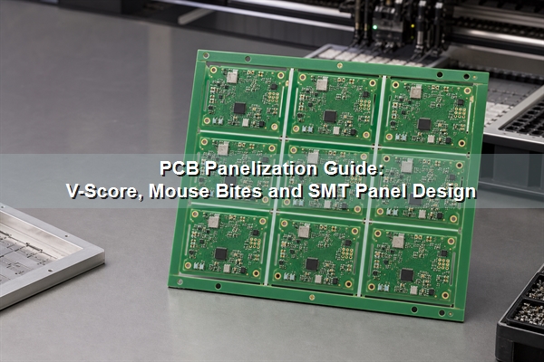
PCB panelization arranges multiple circuit boards within one manufacturing panel so fabrication, solder paste printing, placement, reflow, inspection and handling can process them as a stable unit. A useful panel is not simply the layout that fits the most boards. Its outline, rails, spacing, separation method, tooling features and component clearances must match the fabricator’s CAM rules, the assembly line and the final depaneling process.
What Is PCB Panelization?
PCB panelization converts one PCB design, or a controlled set of compatible designs, into a larger array that production equipment can transport and process. The finished panel normally includes the repeated board images, panel rails, separation features, global fiducials, tooling holes and identification marks. After assembly and testing, the individual boards are separated by V-scoring, routing, punching, sawing or laser cutting as appropriate.
A single PCB may be large and rigid enough to run without a delivery array, but small, narrow, irregular or thin boards often need added support. The phrase panelization construction is sometimes used for the complete arrangement of boards and temporary panel features. Practical PCB panelization guidelines must therefore define both the customer delivery panel and the fabricator-controlled production panel, which may include several delivery panels plus test coupons.
Why Is Panelizing PCB Important for Fabrication and SMT Assembly?
Panelizing PCB designs reduces repeated handling and gives conveyors, printers, placement machines and inspection systems a consistent rectangular workpiece. Several boards can pass through one stencil print, one placement program and one reflow cycle. Panel rails also protect edge components and create room for machine references that would not fit on a small finished board.
The benefit depends on the whole route. A dense array can improve laminate utilization but become too flexible under stencil pressure. A rigid array may process well yet waste material or impose excessive stress during separation. When the same supplier controls FR4 PCB fabrication and PCB assembly, CAM and SMT engineers can review the delivery panel against fabrication tolerances, stencil data, component placement and depaneling access before release.
Which PCB Panelization Methods Should You Choose?
The separation method should be chosen before the array geometry is frozen. The main PCB panelization methods have different shape, spacing, stress and edge-finish limits.
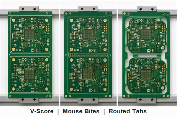
V-scoring: uses straight grooves from opposite sides of the panel. It is space-efficient for rectangular boards with continuous straight separation lines.
Tab routing: routes most of the board outline while leaving solid tabs. It supports irregular contours and allows the tabs to be cut by a router.
Mouse bites: add perforated holes to breakaway tabs for manual separation. A PCB panelization mouse bites pattern must match the fabricator’s drill and routing capabilities.
Laser depaneling: provides a narrow, non-contact cut path for suitable materials and thicknesses, but it needs specialized equipment and process review.
Punching or sawing: can suit stable high-volume geometries, although tooling cost or straight-line limits restrict their use.
The manufacturer should confirm channel width, residual web, tab placement and keepouts rather than relying on a universal online drawing. Material, finished thickness, copper distribution and component layout all change the result.
How Do V-Score and Tab Routing Compare?
The decision starts with board geometry and permitted separation stress. V-score favors straight outlines and high panel utilization. Tab routing accepts complex shapes and controlled tab locations but consumes area for the router path.
Decision factor
V-score
Tab routing / mouse bites
Board outline
Straight, continuous separation lines
Curved or irregular outlines are possible
Board spacing
Boards may share a score line
Routing channel is required
Separation stress
Can flex a longer board edge
Localized at selected tabs
Finished edge
Straight scored edge
Tab witness may remain unless machine-routed flush
Component placement
Needs clearance from the score and flex zone
Needs clearance from tabs, router access and breakout force
Best fit
Rectangular, repeatable arrays
Irregular shapes and selective support points
For more detail on breakout geometry, see the related guides to mouse bites versus V-groove and V-cut PCB depaneling. The production drawing should still use the dimensions approved for the current manufacturer and equipment.
What Panel Rails, Fiducials and Tooling Holes Are Required?
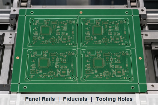
Panel rails create straight conveyor edges, increase stiffness and hold temporary production features. Their width follows the printer, conveyor, fixture and depaneling setup, not a fixed internet value. Rails may also carry global fiducials, tooling holes, barcodes, coupons and orientation marks.
Global fiducials establish panel translation and rotation for vision-guided equipment. An asymmetric arrangement reduces the chance of loading the panel in the wrong orientation. Tooling holes provide mechanical registration where a fixture or process requires it. Local board fiducials may still be needed near fine-pitch BGA, QFN or other placement-critical packages.
The panel data used to manufacture an SMT stencil must use the same board step-and-repeat, origin and orientation as the placement data. A stencil generated from a single-board paste layer cannot be assumed to match a later CAM-created array unless the duplication and datum transformation are controlled.
How Should PCB Panel Size, Spacing and Component Clearance Be Set?
A reliable PCB panel design starts with the usable machine envelope, then reserves rails, separation geometry and component keepouts before calculating the array count. Filling the entire fabrication sheet first can produce a panel that cannot be printed, transported or depanelized safely.
PCB panel size is constrained by every machine that must handle the panel, including fabrication equipment, stencil printers, pick-and-place systems, reflow conveyors, AOI, test fixtures and depaneling equipment. The smallest and largest usable dimensions, conveyor direction and rail requirements should be confirmed with the actual production route.
Board-to-board spacing follows the separation tool. V-score can place straight board edges together, while routing needs a channel wide enough for the selected cutter and positional tolerance. Laser separation may use a narrower path but requires material and thermal-process review. A PCB panelization calculator can estimate how many boards fit, but it cannot see every process restriction or guarantee the lowest finished-board cost.
Component clearance must include the body, solder joints, overhang, tool envelope and expected board flex. Ceramic capacitors, BGA corners, connectors and heavy parts close to a break line deserve particular attention because depaneling strain can damage a solder joint without leaving an obvious board crack. Copper, vias and controlled-impedance structures also need clearance from score grooves, routed channels and mouse-bite holes.
When Can Different PCBs Share One Panel?
Different PCB part numbers can share a panel only when their fabrication and assembly requirements are compatible. A mixed array generally needs the same material system, layer stack, finished thickness, copper weight, surface finish, solder mask process and production quantity ratio. If one design changes, the shared panel and its assembly data may also require revision.
A homogeneous panel containing one repeated design is easier to control, inspect and replenish. A heterogeneous panel can synchronize a product set and improve material utilization, but it may create unwanted inventory if the demand ratio changes. Rotated boards can improve nesting, yet their copper distribution and component orientation should be checked for reflow, wave soldering and inspection consistency.
Rigid-flex PCB and flex PCB panelization need additional attention to stiffeners, coverlay, bend regions, tooling support and final separation. Their temporary support strategy should be reviewed as part of the material and assembly process rather than copied from a rigid FR4 grid.
What Files Define the Panelization of PCB Arrays?
The panelization of PCB arrays should be defined by one controlled data package. At minimum, identify the finished panel outline, board origins, step-and-repeat, routing or scoring paths, tabs, fiducials, tooling holes, rails and critical dimensions. The fabrication data and the drawing must agree.
Gerber or ODB++: copper, mask, legend, profile and panel-level production features.
NC drill and rout files: tooling holes, mouse bites, slots and routed channels.
Pick-and-place data: component coordinates transformed to the panel origin and repeated orientation.
Paste and stencil data: the same array count and datum used by assembly.
Assembly drawing: panel orientation, board references, special handling and depaneling restrictions.
Do not submit a customer-created panel Gerber together with a single-board NC drill or placement file unless the relationship is explicitly controlled. Mismatched repetition counts, origins and rotations are a common source of preventable CAM and assembly questions.
Which PCB Panelization Software and Tools Are Useful?
A PCB panelization tool is useful for layout exploration, but the correct choice depends on who owns the production data. PCB panelization software inside ECAD can preserve design links; CAM software can duplicate manufacturing layers, drill data and net information; a PCB panelization calculator is best treated as an early utilization estimate.
PCB panelization Altium workflows: Embedded Board Array and Draftsman can create repeated arrays and fabrication drawings. Searches for Altium PCB panelization and Altium Designer PCB panelization normally refer to these functions.
PCB panelization KiCad workflows: plugins or hierarchical layout methods can create arrays, but users should verify Gerber, drill, position and reference-designator output. The phrase KiCad PCB panelization describes the same task from the tool-first search direction.
Fusion 360 PCB panelization: users should confirm whether the selected Electronics/EAGLE workflow exports every required manufacturing and assembly layer for the array.
Free PCB panelization software: may be adequate for geometry trials, but output integrity, drill duplication, netlist consistency and revision control still require checking.
Manufacturer CAM: usually offers the strongest alignment with actual material utilization, routing tools, panel borders and production equipment.
Software does not know every shop-specific limit. The released files should be checked in an independent CAM viewer and approved against the manufacturer’s panel drawing.
Should You Panelize the PCB or Let the Manufacturer Do It?
Let the manufacturer create the panel when the main goal is cost-efficient fabrication and the array has no product-specific mechanical constraints. Supply clean single-board data, state whether boards must arrive as a panel or separated, identify the assembly route and approve the returned panel drawing. This lets CAM use current working-panel sizes, routing tools and process margins.
Create and control the panel yourself when the assembly fixture, test nest, barcode position, mixed-design ratio, break sequence or customer equipment requires an exact delivery format. In that case, provide both the panel data and the original single-board source, then allow a DFM review. Ownership of the layout does not remove the manufacturer’s responsibility to flag incompatible geometry.
EBest Circuit (Best Technology) lists PCB dimensions up to 610 x 610 mm, subject to stack-up, material, panel utilization and engineering review. The published PCBA process includes 3D SPI, AOI, X-ray and functional testing. Those capabilities are useful only when the approved panel, stencil, placement data and inspection program share the same revision and datum.
How Does PCB Panelization Affect Cost and Yield?
Panelization changes cost through laminate utilization, machine handling, tooling, assembly cycle time, inspection and depaneling. Increasing the number of boards per panel can reduce handling per board, but a weak or warped array can increase paste defects, placement error or breakage. The lowest material scrap is not always the lowest total cost.
Compare layouts using finished good boards per panel, expected yield and all required operations. Include routing time, score setup, tab finishing, carrier or fixture needs, stencil size, test access and the labor or machine time required to separate boards. A mixed array can reduce material waste while increasing data control and inventory risk.
What Must Be Checked Before a PCB Panel Is Approved?
Approval should freeze the panel revision that fabrication, stencil, placement, inspection and test will use. Review the panel drawing and rendered CAM output together rather than approving a dimension table in isolation.
Overall panel dimensions, thickness, quantity per panel and conveyor direction are stated.
V-score, routing channels, tabs and mouse bites match the intended depaneling process.
Rails, fiducials, tooling holes and orientation marks match SMT equipment and fixtures.
Components, copper and vias have adequate clearance from every separation feature.
Gerber/ODB++, NC drill, stencil, placement and assembly drawings use the same origin, rotation and revision.
The panel remains sufficiently rigid through printing, placement, reflow, inspection and handling.
Mixed designs share compatible stack-up, materials, finish and production ratio.
First-panel separation verifies edge quality, strain-sensitive components and fixture access before volume release.
The related PCB panelization approval guide provides a focused release-control workflow. For the present project, keep the signed panel drawing with the manufacturing package so later revisions cannot silently change the array.
PCB Panelization FAQ
What Is Meant by PCB Panelization?
What is meant by PCB panelization is the temporary grouping of multiple boards into one production unit. The boards remain connected during fabrication or assembly and are separated after the required processes are complete.
Does Every Single PCB Need a Panel?
No. A sufficiently large, rigid and machine-compatible single PCB may run without a delivery array. Small, irregular, thin or edge-sensitive boards usually benefit more from rails and repeated panel processing.
Can a PCB Panelization Calculator Produce Final Manufacturing Data?
It can estimate board count and utilization, but final data still needs routing, score, rail, tooling, fixture and equipment review. Treat the result as a layout proposal rather than automatic production approval.
Can Flex PCB Panelization Use the Same Rules as Rigid FR4?
Not automatically. Flex PCB panelization may use stiffeners, temporary carriers, tooling strips or material-specific separation methods. Bend regions, coverlay and thin-material handling require process-specific review.
Can the PCB Manufacturer Panelize Single-Board Gerbers?
Yes, and this is often the simplest route when the delivery panel has no fixed fixture constraints. State the required panel delivery, assembly process and depaneling preference, then approve the manufacturer’s drawing before production.
Conclusion
Effective PCB panelization connects board geometry with fabrication, SMT handling, separation and data control. Choose the depaneling method first, define rails and machine references, keep every production file on one datum and approve the rendered panel before release. For a DFM review of single-board or controlled panel data, contact EBest Circuit (Best Technology) at sales@bestpcbs.com.
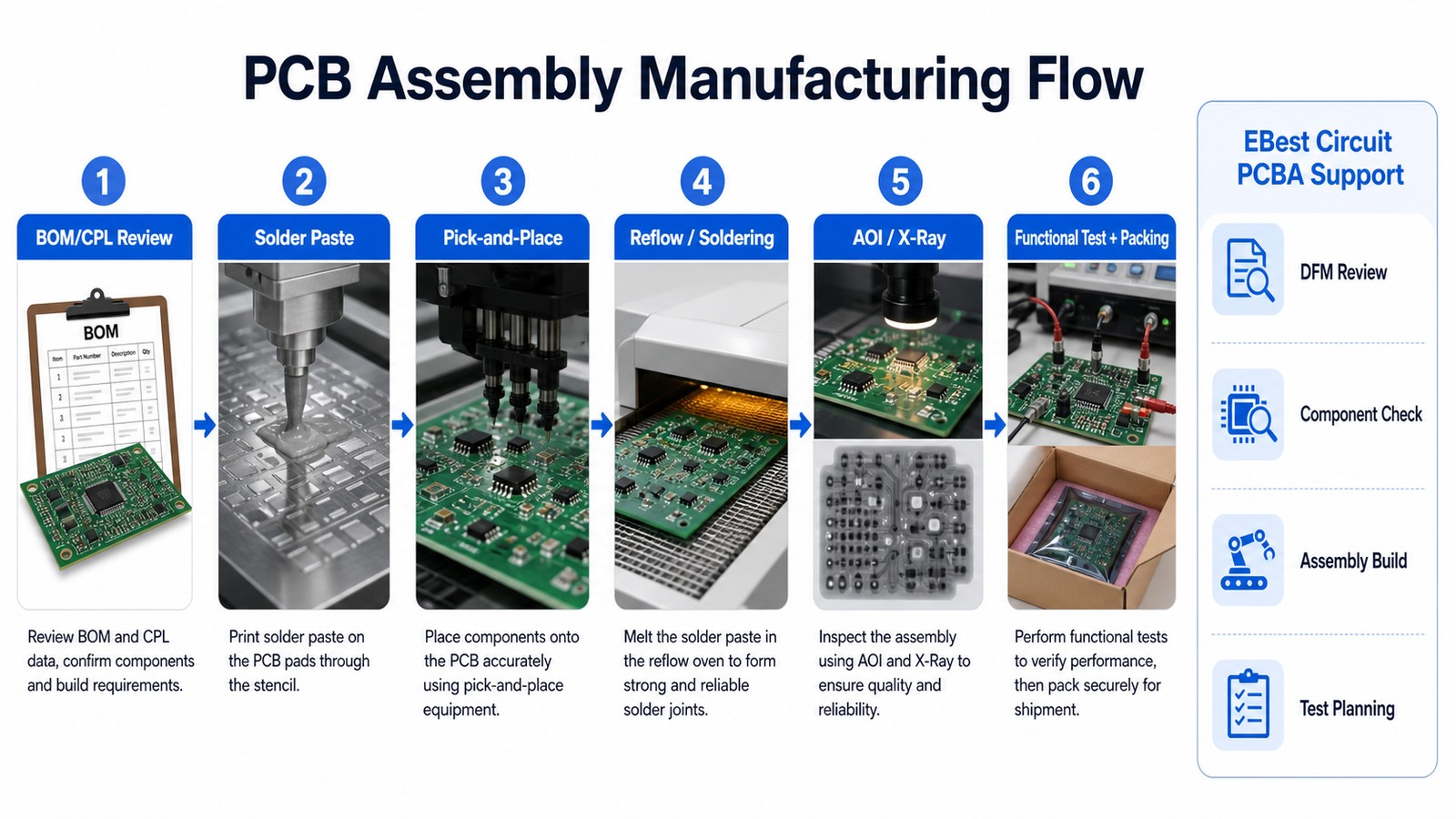
A PCB assembly manufacturer turns bare circuit boards, components and assembly data into working PCBA units. The right partner reviews BOM, CPL, Gerber, assembly drawings, test needs and delivery expectations before production, so buyers know what is included in the quote.
For buyers, PCB assembly is not just component placement. It includes file review, component checking, soldering process planning, inspection, test coordination, packaging and repeat-order control.
PCB assembly projects become expensive when the supplier only quotes placement and ignores the full build package.
BOM alternates, obsolete parts or unclear manufacturer part numbers are found after the order is approved.
CPL data does not match the board revision, causing placement delay or polarity risk.
The quote excludes stencil, inspection, programming, test fixture, packaging or engineering review.
Fine-pitch parts, connectors, BGAs or mixed SMT/PTH parts need more planning than a simple assembly quote shows.
The supplier can build the first batch but does not help stabilize repeat orders.
EBest Circuit supports PCB assembly with DFM review, BOM/CPL checking, PCBA build planning and inspection coordination.
We review Gerber, BOM, CPL, assembly drawings, polarity notes, quantity and test requirements before quote confirmation.
We help buyers align PCB fabrication and PCBA scope instead of treating assembly as a late add-on.
We identify file gaps, component questions and inspection needs early to reduce avoidable schedule changes.
We support prototype, low-volume and repeat PCBA production planning for industrial, telecom, LED, medical electronics and consumer electronics projects.
PCB Assembly Manufacturer in One Practical Answer
A PCB assembly manufacturer provides SMT, through-hole or mixed-technology assembly services for printed circuit boards. The supplier should convert your PCB files, BOM and placement data into assembled boards with clear inspection and test expectations.
What a PCB Assembly Manufacturer Should Review First
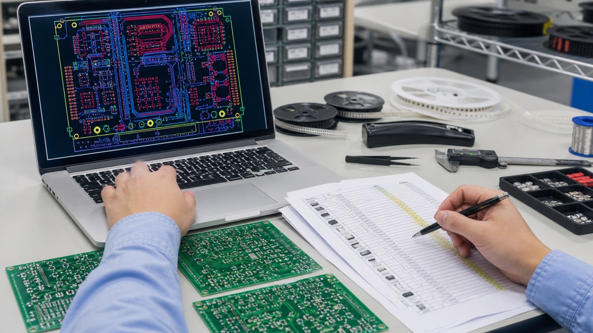
The first review should cover the complete build package, not only the bare PCB. Send Gerber or ODB++, BOM, CPL, assembly drawing, polarity notes, quantity, test requirements and target delivery plan together.
SMT, Through-Hole and Mixed Assembly Options
Most PCBA projects use SMT, through-hole or a mix of both. SMT fits compact electronics and automated placement. Through-hole is common for connectors, terminals and mechanically stressed parts. Mixed assembly requires sequence planning.
Assembly Type
Best Fit
Buyer Check
SMT
Dense electronic assemblies
BOM/CPL accuracy and package orientation
Through-hole
Connectors and stronger mechanical joints
Hole size, clearance and soldering method
Mixed assembly
Boards with SMT plus connectors or terminals
Process order, inspection and test access
BOM and CPL Checks Before Assembly
BOM and CPL review prevents many assembly delays before they reach the production line. Check reference designators, manufacturer part numbers, polarity, package size, rotation, coordinates, substitutions and no-fit parts.
DFM and DFTA Before PCBA Production
Assembly DFM checks whether the design can be built, inspected and tested reliably. Review component spacing, fiducials, tooling rails, stencil needs, thermal pads, connector clearance and test access. For layout readiness, see the PCB design for manufacturability guide.
Need a PCB assembly quote that checks the full build package?
Send Gerber, BOM, CPL, assembly drawings, quantity and test requirements. EBest Circuit can review DFM, component questions, assembly scope and quote readiness.
Component sourcing should be discussed before approval because availability can change assembly cost and lead time. Buyers should define approved alternates, no-substitute parts, consigned parts and sourcing responsibility.
Inspection Methods for PCBA Builds
Inspection should match the component mix and risk level. AOI can check visible solder and placement issues. X-ray may be useful for hidden joints. Functional testing confirms whether the assembly performs the intended task. See the AOI in PCB manufacturing guide for inspection planning.
Prototype, Low-Volume and Repeat PCBA Builds
A good PCB assembly manufacturer should explain how the build stage changes the assembly plan. Prototype assembly focuses on learning and correction. Low-volume builds need repeatability. Production orders need stable files, controlled sourcing and inspection planning.
PCBA cost depends on component count, package type, sourcing, stencil, assembly process, inspection, testing, programming, packaging and quantity. A low placement quote may not include the work needed to deliver reliable assembled boards.
How to Compare PCB Assembly Manufacturers
Compare suppliers by engineering review quality, component handling, assembly process fit, inspection scope and quote clarity. Ask what is included, what is excluded, and what files are needed before the quote becomes final.
What to Send for a PCB Assembly Quote
A complete assembly RFQ should include Gerber or ODB++, BOM, CPL, assembly drawings, polarity notes, quantity, test requirements, programming needs and delivery targets. For bare board support, use EBest Circuit’s PCB manufacturing capabilities and PCBA services.
Use EBest Circuit as your PCB assembly quote benchmark.
A second engineering quote can help you compare BOM/CPL review, assembly scope, inspection, testing and delivery planning before supplier selection.
What does a PCB assembly manufacturer do? It assembles components onto printed circuit boards and may also support BOM review, sourcing, inspection, testing and packaging.
What files are needed for PCB assembly? Send Gerber or ODB++, BOM, CPL, assembly drawings, polarity notes, quantity and test requirements.
Should PCB fabrication and assembly be quoted together? Often yes. Quoting together helps align board design, BOM, placement, inspection and test needs earlier.
Can EBest Circuit support PCB assembly projects? Yes. EBest Circuit can review PCB files, BOM/CPL, assembly scope, inspection needs and RFQ requirements for PCBA builds.
Final RFQ Recommendation
Choose a PCB assembly manufacturer that reviews the whole build package before production starts. That gives you clearer cost, schedule, inspection and repeat-order expectations.
Send your Gerber or ODB++, BOM, CPL, assembly drawings, quantity, component sourcing notes, testing requirements and target delivery plan to sales@bestpcbs.com. EBest Circuit can review your PCB assembly manufacturer requirements and provide a practical quotation path for PCBA production.
Custom PCB assembly services are easier to quote and control when the BOM, design files, sourcing plan and test requirements are clear before production.
Custom PCB assembly services turn a bare printed circuit board, component list and assembly data into a working PCBA built for a specific product. A useful assembly order is not defined only by quantity and delivery date. It depends on a clean BOM, verified footprints, component availability, DFM review, soldering method, inspection plan, functional test needs and clear acceptance criteria.
For buyers and hardware teams, the right question is not only “who can assemble this PCB?” A better question is “what information does the assembly supplier need to build the first batch without guessing?” This checklist explains the files, engineering checks, sourcing decisions, quality controls and RFQ questions that should be settled before custom PCBA production starts.
What Are Custom PCB Assembly Services?
Custom PCB assembly services cover the process of mounting and soldering components onto a customer-specific PCB, then inspecting and testing the assembled board against the product requirement.
The service may include SMT assembly, through-hole assembly, mixed-technology assembly, BGA placement, cable or wire soldering, conformal coating, programming, box-build steps, component sourcing and functional testing. For a simple prototype, the supplier may only need Gerbers, a BOM and a pick-and-place file. For a production PCBA, the supplier also needs revision control, approved alternates, test fixtures, packaging requirements and a clear defect-handling process.
A bare PCB can look correct and still fail after assembly if the footprint, pad design, component height, thermal relief, polarity marking or soldering process was not checked early. That is why custom assembly should be treated as an engineering workflow, not just a labor quote.
Files Needed Before a PCBA Supplier Can Quote Accurately
A PCBA quotation is only reliable when the supplier can see the board design, component demand and assembly method without filling gaps by assumption.
At minimum, send Gerber or ODB++ files, NC drill data, a BOM with manufacturer part numbers, quantity, designator and package, a centroid or pick-and-place file, assembly drawings, polarity notes, special soldering notes, test requirements and the target quantity. If the project has critical parts, include approved substitutes, lifecycle notes and any customer-supplied material plan.
BOM, centroid, Gerber and assembly drawing review should happen before components are purchased or the SMT line is scheduled.
Common quoting problems include obsolete parts, inconsistent package names, missing polarity, a centroid file that does not match the latest Gerbers, unclear do-not-populate parts, no test method, and a requested delivery date that ignores component lead time. Best Technology’s Component Sourcing page is a useful internal reference when a project needs turnkey sourcing instead of consigned parts.
BOM Review Comes Before Assembly Scheduling
BOM review should confirm that every part can be bought, placed, soldered and inspected before the assembly job is released.
A practical BOM review checks manufacturer part numbers, distributor availability, package consistency, moisture sensitivity, polarity, lifecycle risk, RoHS or other compliance needs, approved alternates and customer-supplied parts. It should also separate no-load parts, optional variants and parts that need special storage or handling. For prototypes, this prevents delays. For repeat builds, it reduces the chance of silent substitutions and batch-to-batch variation.
BOM Item
What to Check
Why It Matters
MPN and package
Manufacturer part number, footprint, pin count and package code.
Wrong packages cause placement errors or unusable boards.
Availability
Stock, lead time, MOQ and approved substitutes.
Component shortages can delay assembly more than PCB fabrication.
Polarity and orientation
Diodes, LEDs, ICs, connectors, electrolytic capacitors and batteries.
Orientation mistakes can damage the product during first power-up.
Special handling
MSL level, baking needs, ESD controls and storage limits.
Moisture or handling problems can create hidden reliability defects.
Test relevance
Parts tied to programming, calibration or functional test.
Testing cannot be planned correctly if critical parts are not identified.
DFM and DFA Checks That Prevent Assembly Rework
DFM and DFA checks should focus on placement, solderability, inspection access and test access before the first board enters production.
Confirm solder paste openings for fine-pitch ICs, QFN packages and thermal pads.
Check BGA escape routing, via-in-pad treatment and X-ray inspection needs.
Review component spacing, connector keep-out areas and tall part interference.
Verify fiducials, panel rails, tooling holes and board support for SMT handling.
Check test points for programming, ICT, functional test or power rail measurement.
Review through-hole clearances for wave soldering, selective soldering or hand soldering.
Confirm polarity marks are visible after assembly and not hidden under components.
When the design includes dense IC packages, early review of BGA Assembly requirements can prevent problems with pad design, X-ray inspection, rework access and thermal profile control.
SMT, Through-Hole and Mixed Assembly Need Different Planning
The correct assembly method depends on component package, mechanical strength, thermal demand, production volume and inspection requirements.
Assembly Type
Best Fit
Buyer Check
SMT assembly
Most modern ICs, passives, sensors, communication modules and compact products.
Confirm stencil, fiducials, placement accuracy and reflow profile needs.
Through-hole assembly
Connectors, power parts, large capacitors and mechanically stressed parts.
Confirm wave, selective or manual soldering and keep-out clearance.
Mixed assembly
Boards with both SMT and through-hole devices.
Confirm process order, hand-solder risk and cleaning requirements.
Box-build support
PCBAs that must be wired, enclosed, programmed or packed as a module.
Confirm drawings, cable routing, labeling, fixture needs and final test steps.
If the project must move from engineering samples to repeated builds, Prototype PCB Assembly and Quick Turn PCB Assembly pages are relevant internal references for prototype and schedule-sensitive PCBA planning.
This SMT workflow video is included as a process supplement; the file, BOM, DFM and test requirements still need to be defined in writing before RFQ.
Inspection and Testing Should Be Defined Before Production
Inspection and testing should match the product risk, not a generic pass-fail line in the purchase order.
Typical PCBA checks include solder paste inspection when needed, first-article inspection, AOI, X-ray for BGA or hidden joints, visual inspection, programming, power-on check, ICT, flying probe, functional test, burn-in or environmental screening when the application requires it. The buyer should define which tests are included, which reports are required, and what happens when a board fails.
Functional checks, AOI, X-ray and fixture-based testing should be planned according to the risk level of the PCBA.
For projects where test coverage affects acceptance, Best Technology’s PCB test equipment page can help buyers understand common inspection and test resources. The article should not replace a project-specific test plan, but it gives useful vocabulary for RFQ discussions.
Cost and Lead Time Drivers in Custom PCB Assembly Services
Assembly cost and lead time are usually driven by component sourcing, placement complexity, test requirements and rework risk rather than board quantity alone.
Main cost drivers include BOM line count, fine-pitch packages, BGA or QFN devices, double-sided assembly, through-hole soldering, conformal coating, programming, functional test fixtures, component shortages, consigned material handling, packaging and urgent delivery. A low assembly price can become expensive if it excludes sourcing review, test setup or failure analysis support.
Buyers should ask the supplier to separate PCB fabrication, component sourcing, SMT assembly, through-hole assembly, testing, programming, packaging and freight. That makes it easier to compare quotes and identify where the real risk sits.
RFQ Questions to Ask a Custom PCBA Supplier
Good RFQ questions reveal whether the supplier understands the assembly risk before the purchase order is issued.
Are any parts obsolete, long-lead, high-risk or missing approved substitutes?
Do the BOM, centroid file, Gerbers and assembly drawings match the same revision?
Which DFM or DFA issues should be fixed before production?
Which soldering process will be used for SMT, through-hole and mixed components?
Which inspection steps are included, and which need a separate request?
Can the supplier support first-article approval before the full batch?
What test data, photos, reports or failure feedback will be provided?
How will customer-supplied parts, shortages and alternate parts be controlled?
For turnkey projects, the main service page for PCB assembly support should be reviewed together with the quote, because sourcing, assembly, inspection and testing are connected decisions.
FAQ
What files do I need for custom PCB assembly services?
You usually need Gerber or ODB++ files, NC drill files, a BOM with manufacturer part numbers, a centroid file, assembly drawings, polarity notes and test requirements. For turnkey assembly, include approved substitutes and any customer-supplied material list.
Is custom PCB assembly the same as PCB fabrication?
No. PCB fabrication makes the bare board. PCB assembly mounts and solders components onto that board. A complete PCBA project may include both steps, plus component sourcing, inspection, programming and functional testing.
What causes delays in PCB assembly projects?
Common delays come from obsolete parts, missing BOM data, mismatched file revisions, unclear polarity, unavailable substitutes, DFM problems, missing test fixtures and late design changes. Component sourcing often controls the schedule more than SMT placement time.
Should I use consigned or turnkey PCB assembly?
Use consigned assembly when you already control parts and want the supplier to assemble them. Use turnkey assembly when you want the supplier to source components, manage purchasing risk and coordinate fabrication, assembly and testing.
When is X-ray inspection needed for PCBA?
X-ray inspection is useful for BGA, QFN, hidden solder joints, via-in-pad structures and assemblies where solder quality cannot be judged visually. It should be specified before quotation if it is part of acceptance.
How can I reduce custom PCB assembly cost?
Clean the BOM, approve alternates, avoid unnecessary special handling, design for accessible testing, reduce avoidable hand soldering, confirm footprints early and separate required tests from optional reports. Do not remove checks that protect product reliability.
What should be checked before first-article approval?
Check component values, polarity, solder joints, connector orientation, programming status, power rails, functional behavior, mechanical fit, labeling and packaging. Any deviation should be corrected before the remaining quantity is released.
Final Thoughts
Custom PCB assembly services work best when the supplier receives clear files, a controlled BOM, realistic process requirements and a defined inspection plan before production. A complete RFQ does not slow the project down. It reduces avoidable clarification, rework and delivery risk.
If you are preparing a prototype, pilot build or production PCBA, send your Gerber files, BOM, centroid file, assembly drawings and test requirements to the Best Technology engineering team at sales@bestpcbs.com for review and quotation support.
Soldering flux vs soldering paste is a common question in electronics soldering and PCB assembly. The two materials look related, but they do different jobs.
Flux helps solder flow. It removes oxidation and improves wetting.
Soldering paste, also called solder paste, contains solder alloy powder and flux. It can form solder joints during reflow.
So the simple answer is this: flux helps solder work better, while solder paste provides the solder metal and flux together.
This guide explains the difference, when to use each one, and how to avoid common soldering mistakes.
Soldering Flux vs Soldering Paste: Quick Difference
Soldering flux is not solder. Soldering paste contains solder.
That is the biggest difference.
Item
Soldering Flux
Soldering Paste
Main role
Helps solder flow
Forms solder joints
Contains solder metal?
No
Yes
Contains flux?
Yes
Yes
Common form
Liquid, gel, pen, or paste flux
Gray metallic paste
Best use
Hand soldering, repair, rework
SMT assembly and reflow
Application
Brush, pen, syringe, or bottle
Stencil, syringe, or dispenser
Heating result
Cleans and activates the surface
Melts and creates the joint
Think of flux as the helper. Think of solder paste as the joint-forming material.
Flux alone cannot mount an SMT component. It does not supply metal. Solder paste can mount the component because it contains solder alloy powder.
What Is Soldering Flux?
Soldering flux is a chemical material that removes oxidation and helps solder wet metal surfaces.
Copper pads, wires, and component leads can oxidize. Oxidation makes soldering harder. Solder may bead up or refuse to spread.
Flux helps solve this problem.
During heating, flux does three useful things:
Removes light oxidation
Helps molten solder spread
Protects the hot surface from new oxidation
Technicians use flux for hand soldering, PCB repair, wire tinning, connector soldering, and SMT touch-up.
Flux comes in several forms:
Liquid flux
Flux pen
Gel flux
Paste flux
Rosin flux
No-clean flux
Water-soluble flux
For electronics, use electronics-grade flux. Do not use plumbing flux on PCBs. It can damage copper pads and traces.
What Is Soldering Paste?
Soldering paste is a gray mixture of fine solder alloy powder and flux. It is mainly used in SMT PCB assembly to form solder joints during reflow soldering.
The alloy powder creates the solder joint. The flux inside the paste helps clean the PCB pads and component terminals during heating.
Pick-and-place machines place components on the paste.
Reflow soldering melts the solder particles.
Cooling forms stable solder joints.
This is why solder paste is widely used for ICs, resistors, capacitors, QFN, BGA, and other surface-mount components.
Common Solder Paste Types We Use
In SMT production, lead-free solder paste is commonly used for RoHS-compliant PCB assembly.
Solder Paste Type
Typical Composition
Common Use
SAC305
Sn96.5%, Ag3.0%, Cu0.5%
Standard lead-free SMT assembly
SAC0307-type
Sn99%, Ag0.3%, Cu0.7%
Lead-free SMT projects with different process needs
Sn63/Pb37
Sn63%, Pb37%
Some special or legacy applications
For most standard SMT projects, we prefer high-temperature lead-free solder paste because it provides better wetting, stronger solder joints, and more stable process control. Medium-temperature solder paste is considered only when heat-sensitive components or special requirements make it necessary.
Solder Paste Handling Control
Good solder paste handling helps reduce printing defects and soldering problems.
Control Item
Our Typical Practice
Storage temperature
2–10°C
Warming time before use
About 4 hours
Mixing time before printing
About 3 minutes
These controls help keep the solder paste viscosity stable before stencil printing.
Why Is SPI Inspection Important?
After solder paste printing, SPI inspection checks whether the paste has been applied correctly.
SPI can inspect:
Paste volume
Paste area
Paste height and thickness
Offset
Bridging risk
Missing paste
Insufficient paste
It helps find common SMT printing issues early, such as missing paste, misalignment, solder bridging, insufficient paste, and paste tailing. Our SPI inspection accuracy can reach around 10 μm, helping improve solder joint consistency before component placement and reflow.
Main Differences at a Glance
Solder paste and flux both support soldering. But they do not replace each other.
Comparison Point
Soldering Flux
Soldering Paste
Composition
Flux chemicals only
Solder powder + flux
Main purpose
Improve solderability
Deposit solder and form joints
Used with
Solder wire, solder bars, existing solder
SMT components and PCB pads
Common process
Manual soldering and repair
Stencil printing and reflow
Storage
Usually room temperature
Often refrigerated
Can form a joint alone?
No
Yes
Common risk
Too much residue
Bridging, solder balls, expired paste
The key point is simple: flux prepares the surface. Solder paste creates the connection.
If you only need better solder flow, use flux.
If you need to place SMT components before reflow, use solder paste.
Is Soldering Paste the Same as Flux?
No. Soldering paste is not the same as flux.
Solder paste contains flux, but flux does not contain solder alloy powder.
This causes confusion because some products use similar names. For example:
Solder paste
Soldering paste
Paste flux
Soldering flux paste
Rosin paste flux
These names may sound similar. But they are not always the same product.
Here is the easy way to check:
Product Name
Usually Means
Solder paste
Solder powder + flux
Paste flux
Thick flux only
Liquid flux
Liquid flux only
Flux pen
Flux in pen form
Rosin flux
Rosin-based flux
If the product does not contain solder alloy powder, it cannot work as solder paste.
Always check the datasheet. Real solder paste usually lists alloy type, metal content, particle size, and reflow profile.
When Should You Use Flux?
Use flux when you already have solder metal.
For example, you may use solder wire with a soldering iron. The wire supplies solder. The flux helps it flow.
Use soldering flux for:
Hand soldering
Wire tinning
Through-hole soldering
Connector soldering
PCB pad touch-up
SMT rework
Component replacement
Oxidized pads or leads
Flux is especially useful when the solder does not wet the pad well. It can also help when you repair an old PCB.
For hand soldering, flux plus solder wire often gives better control than solder paste.
When Should You Use Solder Paste?
Use solder paste when you need to place solder on PCB pads before heating.
This is common in SMT assembly. The paste holds components in place before reflow. Then it melts and forms solder joints.
Solder paste gives better volume control. This matters for small pads and dense PCB layouts.
Too much paste can cause bridging. Too little paste can cause open joints. That is why stencil design, paste quality, and reflow profile matter in PCBA production.
Liquid Flux vs Paste Flux
Liquid flux and paste flux both help soldering. The better choice depends on the job.
Flux Type
Best For
Advantage
Liquid flux
Fine-pitch ICs and PCB touch-up
Spreads quickly
Flux pen
Small repair areas
Easy to control
Paste flux
Connectors, wires, and larger pads
Stays in place
Gel flux
Precision SMT rework
Good placement control
Liquid flux works well for small pads and fine-pitch pins. It flows into tight spaces.
Paste flux works better when you need the flux to stay in one area. It helps with connectors, wires, and larger solder joints.
For electronics, no-clean flux and rosin flux are common choices. Water-soluble flux can also work, but it needs proper cleaning.
Storage and Handling Tips
Solder paste needs stricter control than flux.
Most solder paste should stay refrigerated. Many products require 0–10°C / 32–50°F storage. Before use, let it return to room temperature. This helps avoid moisture condensation.
Do not use expired solder paste for production. Expired paste can dry out, separate, or print poorly.
Flux is usually more stable. Many flux products can stay at room temperature. Still, you should seal the bottle or container after use.
Item
Solder Paste
Flux
Typical storage
Refrigerated
Room temperature
Shelf life
Often 3–6 months
Often 6–24 months
Main risk
Drying, separation, oxidation
Solvent loss, contamination
After opening
Control exposure time
Keep sealed
Expired material
Do not use for production
Not recommended
Good handling helps prevent solder defects. It also improves solder joint consistency.
Common Mistakes to Avoid
Many soldering problems come from simple material mistakes.
Avoid these errors:
Using flux as solder paste
Using plumbing flux on electronics
Applying too much flux
Using expired solder paste
Printing too much solder paste
Heating solder paste with the wrong profile
Forgetting to clean flux when cleaning is required
Using cold solder paste directly from the refrigerator
Also avoid assuming that “no-clean” always means “no concern.” In RF, high-voltage, medical, aerospace, or high-reliability electronics, residue still needs review.
FAQs About Soldering Flux vs Soldering Paste
Q1: Can I use flux instead of solder paste? A1: No. Flux cannot replace solder paste because it does not contain solder metal. It can only help solder flow.
Q2: Does solder paste already contain flux? A2: Yes. Solder paste contains solder alloy powder and flux. The flux helps clean the surface during reflow.
Q3: Do I need extra flux with solder paste? A3: Usually no. Fresh solder paste already contains flux. Extra flux may help during rework, but too much can leave residue.
Q4: Can solder paste be used for hand soldering? A4: Yes, but it is not always the best choice. For normal hand soldering, solder wire plus flux gives better control.
Q5: What happens if I solder without flux? A5: Solder may not flow well. You may see poor wetting, weak joints, solder balls, or dull joints.
Q6: Is paste flux the same as solder paste? A6: No. Paste flux is flux in a thicker form. Solder paste contains solder powder and flux.
Q7: Should flux be cleaned after soldering? A7: It depends on the flux type. Rosin and water-soluble flux often need cleaning. No-clean flux may stay on the board, but sensitive circuits still need review.
Q8: Can I use plumbing flux for PCB soldering? A8: No. Plumbing flux can corrode PCB pads and traces. Use electronics-grade flux only.
To sum up, soldering flux and soldering paste are not the same material.
Flux helps solder flow and wet the surface. Solder paste contains solder metal and flux, so it can form solder joints during reflow.
Use flux for hand soldering, repair, and rework. Use solder paste for SMT assembly, stencil printing, and reflow soldering.
Choosing the right material helps reduce bridging, poor wetting, weak joints, and process waste.
For PCB fabrication and PCBA assembly, EBest supports PCB manufacturing, component sourcing, SMT assembly, soldering process review, testing, and production-quality control. Send your Gerber files, BOM, and assembly requirements to sales@bestpcbs.com for project support.
SMT vs SMD is a common topic in PCB assembly. Engineers, buyers, and product developers often see these two terms in BOMs, datasheets, assembly drawings, and PCBA quotations. At first, they may look similar. However, they describe different things.
SMT means Surface Mount Technology. It refers to the process of mounting electronic components directly onto the surface of a PCB.
SMD means Surface Mount Device. It refers to the component itself, such as a resistor, capacitor, diode, IC, LED, or connector.
In simple words, SMT is the assembly process, while SMD is the component used in that process.
Therefore, comparing SMT and SMD is not like comparing two competing technologies. Instead, it means understanding how a process and a component type work together in PCBA manufacturing.
This article explains the real difference between SMT and SMD. It also covers SMT soldering, SMD LED applications, through-hole comparison, and how EBest Circuit (Best Technology) supports SMT assembly and SMD component projects.
What Is SMT in PCB Assembly?
SMT stands for Surface Mount Technology. It is a PCB assembly method that places components directly onto PCB pads. Unlike through-hole assembly, SMT does not require most component leads to pass through drilled holes.
Today, manufacturers use SMT in many electronic products. For example, industrial controllers, LED modules, medical electronics, communication devices, automotive boards, IoT products, and consumer electronics often rely on SMT assembly.
How the SMT Process Works
The SMT process usually includes these steps:
Solder paste printing
SMD component placement
Reflow soldering
AOI inspection
X-ray inspection for special packages
Functional testing when needed
First, the SMT line prints solder paste onto PCB pads through a stencil. Then, pick-and-place machines place SMD components onto the pasted pads. After that, the board enters a reflow oven. The heat melts the solder paste and creates solder joints.
Finally, inspection equipment checks the assembled board. This helps the manufacturer find missing parts, solder bridges, wrong polarity, and other visible defects.
Why SMT Is Important
SMT supports compact PCB design. Also, it improves production speed because automated machines can place many components in a short time.
In addition, SMT works well for high-density layouts. Designers can place small resistors, capacitors, ICs, sensors, and LEDs in limited space. As a result, electronic products can become smaller and lighter.
Simply put, SMT helps modern PCB assemblies become compact, efficient, and production-friendly.
What Is SMD in Electronics?
SMD stands for Surface Mount Device. It means an electronic component designed for surface mounting.
Common SMD components include:
SMD resistors
SMD capacitors
SMD inductors
SMD LEDs
SMD diodes
SMD transistors
SMD ICs
SMD connectors
SMD sensors
SMD crystals and oscillators
These components usually have short leads, metal terminals, flat pads, or solder balls. During SMT assembly, solder connects these terminals to PCB pads.
Common SMD Packages
Many familiar package types belong to the SMD family. For instance, engineers often use 0402, 0603, 0805, SOT-23, QFN, SOP, BGA, and PLCC-2 packages.
Each package has its own size and pad requirement. Therefore, the PCB footprint must match the component datasheet. Otherwise, the board may face soldering issues during assembly.
Why Engineers Use SMD Components
SMD components save PCB space. Moreover, they support automated assembly and allow higher component density.
Another benefit is layout flexibility. Many SMD parts can sit on both sides of the PCB. Because of this, engineers can design smaller boards with more functions.
In short, SMD refers to the part. Meanwhile, SMT refers to the method that places the part onto the PCB.
SMT vs SMD: What Is the Real Difference?
The real difference between SMT and SMD is simple. SMT is a technology, while SMD is a device.
These two terms work closely together. However, they do not mean the same thing.
Item
SMT
SMD
Full Name
Surface Mount Technology
Surface Mount Device
Meaning
PCB assembly process
Electronic component
Main Role
Places parts onto the PCB
Gets placed onto the PCB
Used By
PCBA manufacturers and SMT lines
PCB designers and BOM engineers
Example
Reflow soldering process
SMD resistor, capacitor, IC, or LED
Main Concern
Placement, soldering, inspection
Package, polarity, size, availability
A simple sentence explains the relationship well:
Manufacturers use SMT to assemble SMD components onto a PCB.
For example, your BOM may include 0603 resistors, QFN chips, SOT-23 transistors, and SMD LEDs. All of them are SMD parts. During production, the SMT line places and solders them onto the PCB.
Why the Difference Matters
This difference matters because each team focuses on different details.
PCB designers focus on footprints, pad size, spacing, and polarity marks. Meanwhile, purchasing teams care about component availability, lead time, and substitutes. Production engineers, on the other hand, control stencil design, placement accuracy, reflow profile, and inspection.
Therefore, clear terminology improves communication. It also helps reduce mistakes before production starts.
How Do SMT and SMD Work Together in PCB Assembly?
SMT and SMD work together through the whole PCBA process. One belongs to manufacturing. The other belongs to component selection. Even so, both sides must match well.
Step 1: Select the Right SMD Components
The process starts with component selection. Engineers choose SMD parts based on electrical performance, package size, current rating, thermal needs, cost, and availability.
Then, they create PCB footprints for these parts. Each footprint should follow the component datasheet. Although this step looks simple, it strongly affects assembly quality.
Step 2: Prepare the PCB Layout
Next, designers complete the PCB layout. They check pad size, solder mask openings, component spacing, polarity marks, and silkscreen labels.
In addition, they need to consider manufacturing limits. Very small parts need accurate placement. Fine-pitch ICs need careful solder paste control. High-power SMD parts also need proper thermal paths.
Step 3: Run SMT Assembly
After design approval, the PCBA manufacturer uses the production files to run SMT assembly. These files usually include:
Gerber files
BOM
Pick-and-place file
Assembly drawing
Testing notes
Special process requirements
The SMT line prints solder paste, places components, and runs reflow soldering. After soldering, inspection equipment checks the finished joints.
Step 4: Inspect and Test the PCBA
AOI checks common issues such as missing parts, wrong polarity, component shift, solder bridges, and insufficient solder.
For BGA, QFN, LGA, and other hidden-joint packages, X-ray inspection gives a clearer view. Finally, functional testing confirms whether the assembled board works as expected.
As a result, SMT and SMD form one connected workflow:
When every step aligns, the final product becomes easier to manufacture and scale.
SMT vs SMD Soldering: How Does the Assembly Process Work?
People often search for SMT vs SMD soldering because they want to know how SMD parts attach to a PCB.
In most production projects, manufacturers use reflow soldering for SMD components. This method creates stable solder joints and supports automated production.
Process Step
What Happens
Why It Matters
Solder Paste Printing
The stencil applies solder paste to PCB pads
Controls solder volume
SMD Placement
Machines place components onto the pads
Improves position accuracy
Reflow Soldering
Heat melts the solder paste
Forms solder joints
AOI Inspection
Cameras check visible defects
Finds missing parts and solder issues
X-ray Inspection
X-ray checks hidden joints
Supports BGA and QFN inspection
Functional Testing
Testers check board performance
Confirms product function
Stencil Design
Stencil design strongly affects soldering quality. If the stencil opening is too large, excess solder may create bridges. However, if the opening is too small, the joint may lack enough solder.
Therefore, manufacturers need to control stencil thickness and aperture size carefully.
Footprint Accuracy
The PCB footprint must match the SMD package. Otherwise, the part may shift, lift, or solder poorly.
For example, small passive components may suffer from tombstoning when pad design or thermal balance is poor. Fine-pitch ICs may also develop solder bridges when pad spacing and solder volume do not match.
Reflow Profile
The reflow oven needs a suitable temperature curve. A good profile helps solder paste melt, flow, and cool in a controlled way.
At the same time, it protects sensitive components from excessive heat. Therefore, reflow control plays a major role in PCBA reliability.
Overall, SMD soldering is not just a heating process. Instead, it combines PCB design, solder paste, stencil control, placement accuracy, thermal profiling, and inspection.
SMT vs SMD vs THT: Which One Should You Choose?
To understand SMT and SMD better, it helps to compare them with THT.
THT means Through-Hole Technology. In this method, component leads pass through PCB holes. Then, solder connects the leads to the board.
Today, many PCBA projects use both SMT and THT. SMT handles compact parts. Meanwhile, THT handles parts that need stronger mechanical support.
Item
SMT / SMD
THT
Component Position
On the PCB surface
Through PCB holes
Assembly Method
Mainly automated
Manual, wave, or selective soldering
PCB Space
Saves space
Needs more space
Component Density
High
Lower
Mechanical Strength
Good for many parts
Stronger for heavy parts
Common Uses
ICs, resistors, capacitors, LEDs, sensors
Connectors, terminals, transformers, switches
Production Efficiency
High
Usually lower
When SMT Works Better
SMT works well for compact and high-density products. Also, it supports fast production and automated inspection.
For example, a medical sensor board, LED control board, or communication module can benefit from SMT assembly.
When THT Still Makes Sense
THT still has value in many designs. Large connectors, terminal blocks, transformers, and mechanical switches may need stronger support.
For instance, an industrial control board may use SMD ICs and capacitors. However, it may still keep through-hole terminals for field wiring.
Best Choice for Real Projects
In many cases, the best answer is not SMT or THT alone. A mixed assembly often works better.
Designers can use SMD parts for compact circuits and THT parts for mechanical strength. As a result, the PCB gains both high density and practical durability.
SMT vs SMD LED: What Should LED Product Designers Know?
LED products often use both SMT and SMD terms. Many LED modules, lighting boards, display panels, and automotive lighting boards use SMD LEDs assembled by SMT.
Again, the meaning stays clear:
SMD LED means the LED component.
SMT means the process that mounts the LED onto the PCB.
Common SMD LED Packages
Common SMD LED packages include 2835, 3528, 5050, 5730, 3014, and PLCC-2. Designers use them in LED strips, signage, display products, backlights, and indicator lights.
Each LED package has its own pad layout, polarity, brightness level, and thermal behavior. Therefore, the PCB design should match both electrical and thermal needs.
Thermal Design Matters
LEDs generate heat during operation. If the PCB cannot move heat away efficiently, brightness and service life may drop.
For standard LED products, FR4 may work well. However, higher-power LED products often need aluminum PCB or copper-based PCB. In demanding applications, ceramic PCB can also support better thermal performance.
Assembly Details for LED Boards
LED PCB projects need careful control of several points:
LED package size
Polarity marking
Pad design
Solder paste volume
Thermal pad connection
Copper area for heat spreading
PCB material selection
LED spacing
Reflow profile
For example, PLCC-2 is a common SMD LED package. SMT equipment can place it efficiently. Even so, the footprint and polarity marks must be correct.
Therefore, LED designers should not only ask, “Which SMD LED should I choose?” They should also ask, “Can this PCB design support stable SMT assembly?”
How Can EBest Circuit (Best Technology) Support Your SMT Assembly and SMD Component Project?
Understanding SMT and SMD helps you make better technical decisions. However, real project success depends on execution.
A PCBA project involves design review, BOM checking, component sourcing, PCB fabrication, SMT assembly, inspection, testing, and delivery coordination. Therefore, a capable manufacturing partner can save time and reduce production risk.
Engineering Review Before Production
EBest Circuit (Best Technology) supports customers with engineering-driven PCB and PCBA manufacturing services.
Before production, our engineering team can review Gerber files, BOM, pick-and-place files, assembly drawings, and special process notes. During this review, we check pad design, package matching, spacing, polarity marks, stencil openings, panelization, and other assembly details.
As a result, customers can find many potential issues before the SMT line starts.
BOM Review and Component Sourcing
SMD component supply can affect cost, delivery, and production stability. Therefore, BOM review matters.
EBest Circuit (Best Technology) can help check package consistency, component availability, lead time, and alternative options. This support helps customers prepare for prototype builds and future production.
One-Stop PCB and PCBA Support
Many customers prefer one integrated workflow. For that reason, EBest Circuit (Best Technology) can support PCB fabrication, component sourcing, SMT assembly, through-hole assembly, inspection, and testing.
This approach reduces handoffs. It also keeps communication clearer from design files to finished PCB assemblies.
Prototype to Mass Production
New products often start with samples. After testing, customers may move to small-batch or mass production.
EBest Circuit (Best Technology) can support this full path. Our team helps customers review manufacturability, improve assembly stability, and prepare for repeat production.
Quality Inspection and Testing
Depending on the project, quality control can include first article inspection, AOI, X-ray inspection, visual inspection, and functional testing.
For boards with BGA, QFN, or other hidden solder joints, X-ray inspection helps confirm solder quality more clearly.
If you are working on an SMD component project and need reliable SMT assembly support, send your Gerber files, BOM, pick-and-place file, quantity, and assembly requirements to sales@bestpcbs.com. EBest Circuit (Best Technology) can review your project and provide a practical quotation for PCB fabrication and PCBA assembly.
FAQs About SMT vs SMD
1. Is SMT a component or a process? SMT is a process. The full name is Surface Mount Technology. Manufacturers use it to mount components directly onto PCB surfaces.
2. Is SMD the same as SMT? No. SMD means Surface Mount Device, while SMT means Surface Mount Technology. In simple terms, SMD is the part, and SMT is the process.
3. Can technicians solder SMD components by hand? Yes. Technicians can hand-solder some larger SMD components during repair, testing, or prototype work. However, automated SMT assembly gives better speed and consistency for production.
4. Do all modern PCBs use SMD components? Many modern PCBs use SMD components, but not every board uses only SMD parts. Some designs still include through-hole connectors, terminals, switches, or power parts.
5. What files does a manufacturer need for SMT assembly? A PCBA manufacturer usually needs Gerber files, BOM, pick-and-place file, assembly drawing, quantity, and testing requirements.
6. Why do engineers choose SMD components? Engineers choose SMD components because they save space, support automated assembly, and fit high-density PCB layouts.
7. Is SMT better than through-hole assembly? SMT works better for compact and automated assembly. However, through-hole assembly works well for heavy parts or components that need strong mechanical support.
8. What causes SMT soldering defects? Common causes include poor stencil design, wrong pad size, inaccurate placement, unsuitable reflow profile, dirty pads, or mismatched component packages.
9. Can EBest Circuit support both SMT and through-hole assembly? Yes. EBest Circuit (Best Technology) can support PCB fabrication, SMT assembly, through-hole assembly, component sourcing, inspection, and testing.
10. How can I get a quotation for an SMT assembly project? You can send Gerber files, BOM, pick-and-place file, quantity, and testing requirements to sales@bestpcbs.com. The team will review your files and provide a quotation.
SMT (Surface Mount Technology) is the dominant assembly method in modern electronics manufacturing, enabling compact, high-reliability products. Mastering SMT fundamentals and processes is critical for engineers, manufacturers, and buyers seeking consistent quality in electronic assemblies.
What is SMT?
SMT stands for Surface Mount Technology, a core electronic assembly process that mounts surface-mount components (SMDs) directly onto the surface of printed circuit boards (PCBs). It replaces traditional through-hole technology, offering higher assembly density and production efficiency for most electronic devices.
Why is SMT Widely Adopted?
Enables smaller, lighter electronic products with 40-60% volume reduction compared to through-hole designs.
Supports high-volume automation, cutting production costs by 30-50% in mass manufacturing.
Delivers better high-frequency performance and lower electromagnetic interference (EMI).
SMT Meaning
SMT is the abbreviation of Surface Mount Technology, referring to the set of techniques for mounting and soldering SMDs on PCB surfaces without drilling insertion holes. Its core purpose is to achieve reliable electrical and mechanical connections between components and PCBs efficiently.
Key Terminology in SMT
SMD: Surface Mount Device, the components used in SMT assembly (resistors, capacitors, ICs, etc.).
PCB: Printed Circuit Board, the base for mounting SMT components.
Reflow Soldering: The heating process that melts solder paste to bond SMDs to PCB pads.
Definition of SMT
Surface Mount Technology (SMT) is a standardized electronic assembly process that involves applying solder paste to PCB pads, precisely placing SMDs onto the paste, and heating the assembly to form permanent solder joints. It is defined by IPC standards as a high-density, automated assembly method for modern electronics.
Core Characteristics of SMT
SMT eliminates the need for PCB hole drilling for component leads, relying on surface tension and solder paste adhesion to secure components. This results in lower PCB material usage, faster production cycles, and reduced solder joint defect rates compared to traditional methods.
What is SMT in Electronics
In electronics, SMT is the primary method for assembling PCBs in consumer devices, industrial controls, medical equipment, and communications hardware. It enables the miniaturization of high-performance electronics, from smartphones to 5G base stations.
Common Electronic Applications of SMT
Consumer electronics: Smartphones, laptops, wearables, and televisions.
Industrial electronics: PLCs, sensors, and automation controllers.
Medical devices: Diagnostic tools, wearable monitors, and imaging equipment.
What is SMT in Manufacturing
In manufacturing, SMT is a streamlined, automated process that integrates multiple stages—from solder paste printing to inspection—to produce consistent PCB assemblies at scale. It is a cornerstone of lean manufacturing for electronic components.
SMT Manufacturing Workflow Goals
Achieve high throughput: Up to 30,000 components per hour with advanced placement machines.
Maintain low defect rates: Targeting <10 ppm (parts per million) for critical applications.
Ensure process repeatability: Complying with IPC-A-610 and IPC-7351 standards.
Basic SMT Process Flow
The basic SMT process consists of 6 sequential stages, with each step directly affecting final assembly quality. Front-end process control is critical to reducing defects and ensuring reliability.
What Are the Core Stages of SMT?
Solder Paste Printing: Apply solder paste to PCB pads using a stencil, the first gate for welding quality. Laser-cut stencils (±5μm precision) and SPI (Solder Paste Inspection) are mandatory for high-reliability projects.
Component Placement: Use automated machines to place SMDs onto solder paste, requiring repeat accuracy ≤±25μm for 0201-sized components and fine-pitch devices.
Reflow Soldering: Heat the assembly to melt solder paste, forming permanent joints. Custom temperature profiles are needed for different PCB thicknesses and component types.
Inspection & Testing: Combine AOI (surface defects), X-ray (BGA/QFN bottom joints), and FCT (functional verification) to catch hidden issues.
Cleaning (Optional): Remove flux residues via water or semi-aqueous cleaning, tested per IPC-TM-650 for ion contamination.
Reliability Enhancement: Implement ESD protection and underfill for advanced packages to improve long-term stability.
SMT Placement Process
The SMT placement process is a precision-driven step that bridges solder paste printing and reflow soldering, directly impacting component alignment and solder joint integrity.
How to Ensure Accurate SMT Placement?
Machine Calibration: Regularly calibrate placement machines to maintain ±25μm repeat accuracy, replacing worn nozzles to avoid component slippage.
Component Recognition: Use advanced vision systems to identify odd-form components and black-body devices, reducing placement errors.
Double-Side Placement: For double-sided PCBs, prioritize lighter components first to prevent displacement during reflow.
Real-Time Monitoring: Integrate MES systems to track placement parameters, enabling immediate adjustments for offset or misalignment.
Key Advantages of SMT Over Through-Hole Technology
SMT outperforms traditional through-hole technology in most modern electronics, offering irreplaceable benefits for miniaturization and mass production.
SMT vs. Through-Hole: Core Differences
Metric
SMT
Through-Hole
Component Density
40-60% higher, enabling miniaturization
Low, limited by hole spacing
Production Cost
30-50% lower in high-volume manufacturing
Higher due to manual insertion
High-Frequency Performance
Superior, lower EMI
Poor, lead inductance affects signals
Common SMT Defects and Troubleshooting Tips
Most SMT defects stem from process deviations in printing, placement, or reflow. Targeted troubleshooting reduces rework rates and improves consistency.
How to Fix Top SMT Defects?
Open Joints/Voids: Adjust stencil aperture and reflow profile; ensure solder paste freshness (≤3 months shelf life).
Bridging: Reduce stencil aperture size and optimize printing pressure to avoid excess solder paste.
Tombstoning: Balance solder paste volume on component pads and adjust placement accuracy to ≤1/3 pad offset.
Cold Solder: Extend reflow soak time to fully activate flux, ensuring peak temperature (240-250℃ for SAC305).
Critical Factors for High-Quality SMT Assembly
Achieving high-quality SMT assembly requires a combination of equipment precision, process control, and material management, aligned with IPC standards.
What Drives SMT Assembly Quality?
Material Control: Use low-residue solder paste and ESD-safe packaging for sensitive components.
Process Documentation: Record SPI/AOI reports, X-ray images, and reflow curves for full traceability.
Operator Training: Certify staff on IPC-A-610 standards to identify and resolve minor process issues.
Nitrogen Reflow: Adopt nitrogen atmosphere for automotive/medical electronics to reduce oxidation and voids.
SMT FAQ
Below are answers to common SMT questions, addressing pain points in process optimization and quality control.
Frequently Asked Questions About SMT
What is the acceptable void rate for SMT joints? Industrial-grade applications require <25% void rate for BGA/QFN components, tested via X-ray.
How often should SMT stencils be cleaned? Clean stencils every 50-100 prints to prevent paste buildup and aperture clogging.
Can SMT handle double-sided PCBs? Yes—use low-temperature solder paste for the second side to avoid reflowing existing joints.
What’s the difference between leaded and lead-free SMT? Lead-free (SAC305) requires higher peak temperatures (240-250℃) vs. leaded (210-220℃).
How to reduce SMT rework rates? Implement SPI at the front end—printing defects account for 70% of total SMT issues.
Is underfill necessary for SMT? It’s mandatory for fine-pitch BGA and automotive electronics to improve shock and vibration resistance.
What standards govern SMT assembly? IPC-A-610 (acceptability) and IPC-7351 (component land patterns) are industry benchmarks.
Future Trends of SMT Technology
SMT technology is evolving to meet demands for advanced packaging, high reliability, and smart manufacturing in 2026 and beyond.
What’s Next for SMT?
Advanced Packaging Integration: Merging SMT with SiP/Chiplet technologies for high-density, high-performance electronics.
Smart Factory Adoption: Full integration of AI-driven AOI, real-time process monitoring, and MES systems for data-driven optimization.
Automotive-Grade Focus: Enhancing SMT for AEC-Q100/Q200 compliance, with improved thermal and vibration resistance.
On-Demand Manufacturing: Flexible SMT lines to support low-MOQ, fast-turnaround projects for AIoT and wearables.
We provide high-quality SMT assembly services, adhering to IPC standards and advanced process controls to ensure reliability for automotive, medical, and industrial electronics. If you need SMT solutions, place your order with us today—reach out via email at sales@bestpcbs.com.
This website uses cookies to enhance your experience, remember your preferences, and help us understand how visitors use our site. You can accept all cookies, reject non-essential cookies, or manage your settings.
This website uses cookies to improve your experience while you navigate through the website. Out of these cookies, the cookies that are categorized as necessary are stored on your browser as they are essential for the working of basic functionalities of the website. We also use third-party cookies that help us analyze and understand how you use this website. These cookies will be stored in your browser only with your consent. You also have the option to opt-out of these cookies. But opting out of some of these cookies may have an effect on your browsing experience.
Necessary cookies are absolutely essential for the website to function properly. These cookies ensure basic functionalities and security features of the website, anonymously.
Cookie
Duration
Description
cookielawinfo-checkbox-analytics
11 months
This cookie is set by GDPR Cookie Consent plugin. The cookie is used to store the user consent for the cookies in the category "Analytics".
cookielawinfo-checkbox-functional
11 months
The cookie is set by GDPR cookie consent to record the user consent for the cookies in the category "Functional".
cookielawinfo-checkbox-necessary
11 months
This cookie is set by GDPR Cookie Consent plugin. The cookies is used to store the user consent for the cookies in the category "Necessary".
cookielawinfo-checkbox-others
11 months
This cookie is set by GDPR Cookie Consent plugin. The cookie is used to store the user consent for the cookies in the category "Other.
cookielawinfo-checkbox-performance
11 months
This cookie is set by GDPR Cookie Consent plugin. The cookie is used to store the user consent for the cookies in the category "Performance".
viewed_cookie_policy
11 months
The cookie is set by the GDPR Cookie Consent plugin and is used to store whether or not user has consented to the use of cookies. It does not store any personal data.
Functional cookies help to perform certain functionalities like sharing the content of the website on social media platforms, collect feedbacks, and other third-party features.
Performance cookies are used to understand and analyze the key performance indexes of the website which helps in delivering a better user experience for the visitors.
Analytical cookies are used to understand how visitors interact with the website. These cookies help provide information on metrics the number of visitors, bounce rate, traffic source, etc.
Advertisement cookies are used to provide visitors with relevant ads and marketing campaigns. These cookies track visitors across websites and collect information to provide customized ads.