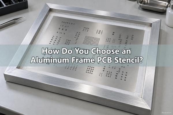
An aluminum frame PCB stencil holds a patterned metal foil under tension so solder paste can be printed onto PCB pads before component placement. The aluminum is the support frame, not normally the printing foil. At EBest Circuit (Best Technology), we supply custom SMT stencils and PCB assembly support. For your project, the useful starting points are printer compatibility, aperture geometry, foil thickness and the final panel layout.
What Is an Aluminum Frame PCB Stencil?
A framed PCB stencil combines three working parts: a rigid frame, a tensioned mesh border and a thin metal foil containing openings that correspond to the solder-paste pattern. The squeegee moves paste across the foil; the openings control where paste reaches the board. After separation, the paste deposits remain on the pads.
The distinction between frame material and PCB stencil material matters when ordering. Aluminum provides a lightweight, rigid support. Stainless steel is commonly used for the PCB stencil foil because it can be fabricated with fine openings and withstand repeated printing and cleaning. A steel foil does not turn the finished circuit board into an aluminum PCB.
A PCB framed stencil is a complete mounted tool, whereas a stencil blank is an unpatterned starting material. If you need a working circuit board stencil, specify the aperture file and mounting arrangement, not just the frame dimensions.
Framed vs Frameless Stencil: Which Suits Your Production?
A permanently framed tool is useful for repeat builds on compatible equipment. A frameless foil can suit either a manual fixture or a reusable tensioning system, but those are different setups. Frameless does not automatically mean unsuitable for production.
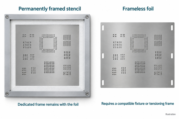
| Option | Best fit | What to check |
|---|---|---|
| Permanently framed stencil | Recurring assemblies with a dedicated tool | Printer fit, stored-frame space, mesh and bond condition |
| Frameless foil in a reusable frame | Multiple designs sharing compatible tensioning hardware | Foil mounting interface, tensioning procedure and changeover time |
| Unframed foil in a manual fixture | Low-volume builds and development work | Flat support, registration and repeatability of the fixture |
For a frameless PCB stencil printer, confirm the foil attachment system before ordering. A foil made for one tensioning system may not fit another. Prototype SMT stencils should therefore be selected around the intended printing process, not around a fixed prototype-versus-production label.
What Frame Size Fits Your Stencil Printer?
There is no single PCB stencil standard size that fits every printer. The outer frame must fit the machine clamps, while the usable printing area must accommodate the complete panel and squeegee travel. Frame profile, thickness, mounting direction and underside-cleaning clearance also affect compatibility.
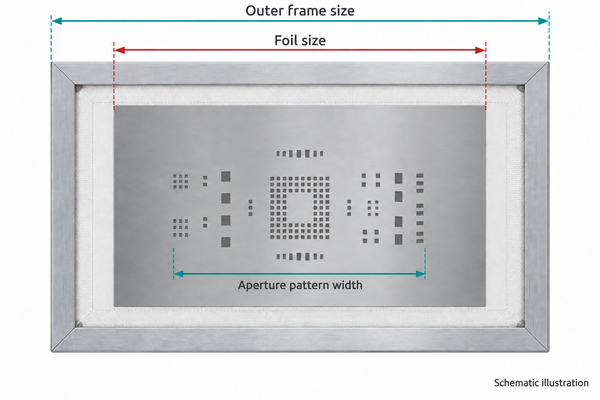
An SMT stencil frame drawing should distinguish the outer frame size, foil size and aperture-pattern envelope. The actual printable area is further limited by bonding margins and the printer mechanism; it is not simply the entire foil. Send the printer model or approved mounting drawing instead of ordering a frame from PCB length and width alone.
A PCB stencil holder or PCB stencil jig must support registration without bending the foil or board. For our FR4 printed circuit boards, use the released panel drawing, including rails, orientation and fiducials, when preparing the stencil. Changing the panel after cutting can make an otherwise accurate stencil unusable.
How to Choose PCB Stencil Thickness?
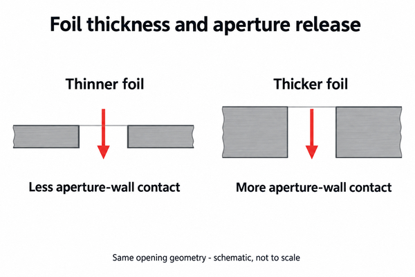
Choose thickness from the paste-volume requirements of the component mix and the release behavior of the smallest openings. A thicker foil provides more theoretical paste volume for the same aperture, but also increases the wall area that the paste must release from. More thickness is not automatically better.
Our custom SMT stencil options cover a foil-thickness range of 0.10-0.60 mm across different stencil applications, subject to engineering review. This capability range is not a recommended thickness range for every fine-pitch SMT board. We also offer step-up and step-down stencil options where different areas need different deposit volumes.
For mixed fine-pitch ICs and larger terminals, evaluate a uniform foil first, then consider local thickness changes if the requirements conflict. Step locations need clearance from nearby apertures and suitable squeegee access. Component pitch alone is not enough to select PCB stencil thickness.
How Does SMT Stencil Aperture Design Affect Paste Release?
SMT stencil aperture design determines both deposit geometry and release conditions. For a rectangular opening with length L, width W and foil thickness t, area ratio is LW / [2t(L + W)]. Aspect ratio is W/t when W is the smaller opening dimension. These describe different geometric relationships.
| Illustrative opening | Foil thickness | Area ratio | Theoretical aperture volume |
|---|---|---|---|
| 0.30 × 0.60 mm | 0.10 mm | 1.00 | 0.018 mm³ |
| 0.30 × 0.60 mm | 0.15 mm | 0.67 | 0.027 mm³ |
These calculated values illustrate geometry, not a guaranteed process window or measured deposit. Actual transfer depends on paste, aperture-wall condition, separation settings and board support. A PCB stencil thickness calculator cannot replace a print trial on the intended assembly.
For large thermal pads, multiple smaller windows may help distribute paste more appropriately than one large opening. For small pads, excessive aperture reduction can make release harder. PCB stencil design should use the component manufacturer’s land-pattern guidance, target deposit and assembly process together; a universal reduction percentage is not suitable for every footprint.
Which Fiducials and Panel Details Must Match?
PCB stencil fiducials let the printer align the foil pattern to the board. Their locations, optical contrast and marking method must suit the vision system. A fiducial is not necessarily an open hole: etching, filling or other marking arrangements depend on the printer and stencil specification.
For double-sided assemblies, identify top and bottom paste files explicitly and confirm viewing direction. Do not mirror a file merely because it is named bottom. The manufacturing output convention and assembly orientation must agree. When both sides share one foil, the printer’s working area, orientation and separation between patterns need approval.
Keep the PCB paste layer, panel drawing and assembly revision synchronized. The solder-mask layer is not a substitute for the paste layer: mask openings expose board features, while paste apertures define deposits for assembly.
How Is a Laser Cut PCB Stencil Made?
A laser cut PCB stencil is produced by cutting the approved aperture pattern into metal foil, applying the specified finishing operations and mounting the foil to its support system. In a permanently framed construction, the foil and mesh bond must maintain the required tension and flatness during use.
Our PCB stencil service includes laser-cut, etched, framed and unframed constructions, as well as electropolishing options. For a laser cut SMT stencil, electropolishing can improve aperture-wall condition, but it does not correct the wrong aperture geometry, foil thickness or panel file. The finishing requirement belongs in the order specification.
Before release, agree on the features that need verification: aperture dimensions and positions, foil thickness, image orientation, frame compatibility, bond condition and tension where specified. For fine-feature work, clarify the measurement method and acceptance criteria rather than assuming the word precision defines them.
How to Use a PCB Stencil?
The basic sequence is alignment, printing, controlled separation and deposit inspection. For a new framed tool, a short first-article print check is more useful than assuming that successful clamping proves process readiness.
- Confirm the stencil revision, print side and matching PCB panel.
- Support the board and align the apertures to the pads using the printer’s specified registration method.
- Apply compatible solder paste and use the established squeegee and separation settings for the assembly.
- Inspect deposit alignment, bridging, missing paste and consistency before placing components.
- Adjust the process or aperture design from the observed defect, rather than compensating for every problem with more pressure.
SMT solder paste stencils are printing tools, not reflow fixtures. The stencil is removed before placement and reflow. Through our PCB assembly services, we support SMT, through-hole and mixed assemblies; discuss stencil supply together with your assembly files when you need a coordinated PCB and PCBA order.
How Should Framed Stencils Be Cleaned and Stored?
Use a cleaning method compatible with the solder paste, foil, mesh and bonding adhesive. Residue inside an aperture can reduce the next deposit, while contamination beneath the foil can contribute to smearing. Follow the applicable cleaning-equipment and chemistry instructions, and protect personnel according to the relevant safety information.
Do not scrape fine openings with tools that can alter their geometry. After cleaning, check for blocked apertures, dents, corrosion, lifted bonding and mesh damage. A visibly clean foil is not automatically a flat, tensioned tool.
Store each tool by design, side and revision in a protected SMT stencil rack or equivalent support. Prevent contact with the active foil area. Reuse depends on condition and validated printing performance, not a universal number of print cycles. A replacement foil must also match the original mounting system.
What Affects the Price of a Framed PCB Stencil?
Price depends on frame size, foil specification, aperture complexity, finishing, step features, inspection requirements and delivery arrangements. A low tool price can be poor value if it requires a new holder, cannot fit the printer or has to be remade after a panel revision.
Compare quotations against the same drawing and scope. Ask whether the price includes the aluminum frame, patterned foil, mounting, specified finishing and inspection. For repeat orders, confirm whether an existing frame can be reused and whether that service is actually included.
For suitable stencil orders, we can provide turnaround as fast as one working day. Availability depends on the design, finishing and order review; production time is separate from transport time. Tell us the required arrival date so that the quotation can address both.
What Files Do We Need for Your Custom Stencil?
For a custom aluminum frame PCB stencil, send the released paste-layer data and final panel information first. We accept Gerber and supported PCB/CAD design files. A PDF can explain dimensions and notes, but a drawing alone may not contain the complete aperture geometry needed for manufacture.
| Input | Include |
|---|---|
| Design identity | Part number, revision, top/bottom side and units |
| Aperture data | Paste Gerber or supported design files, approved modifications and critical features |
| Panel and alignment | Final panel drawing, rails, fiducials and print orientation |
| Printer interface | Machine model, outer frame dimensions, frame profile and clamping requirements |
| Foil and finishing | Requested thickness, step regions, surface treatment and inspection criteria |
| Order scope | Quantity, stencil-only or PCB/PCBA supply, destination and required arrival date |
If the thickness or aperture treatment is not yet defined, identify the fine-pitch devices and larger solder-volume features for review instead of guessing a specification. Send your aluminum frame PCB stencil requirements to sales@bestpcbs.com. Our team can discuss the stencil construction and manufacturing scope with you before quotation.