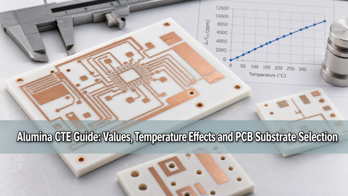
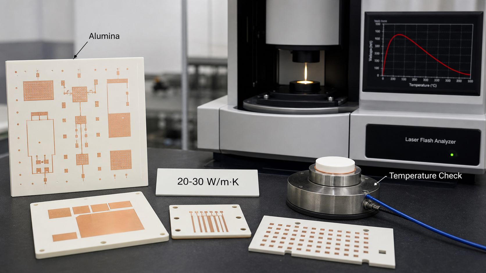
Alumina heat conductivity describes how well aluminum oxide ceramic transfers heat through its structure. For PCB and electronic packaging work, dense alumina substrates are commonly discussed around 20-30 W/m·K at room temperature, depending on purity, density, microstructure and supplier data. That is far above standard FR4, but far below aluminum nitride, so the right choice depends on heat load, insulation, cost, copper design and the complete thermal path.
Alumina is attractive because it combines useful thermal transfer with strong electrical insulation, mechanical hardness, chemical stability and mature ceramic PCB processing. In a real board, however, the material value alone does not determine device temperature. Ceramic thickness, copper coverage, solder or sinter layer, interface material, heat sink flatness and airflow all change the final result.
What Is Alumina Heat Conductivity?
Alumina heat conductivity is the rate at which alumina, also known as aluminum oxide or Al2O3, conducts heat. In engineering data sheets it is usually expressed as thermal conductivity in W/m·K. A higher value means heat can move through the material more easily under the same temperature gradient.
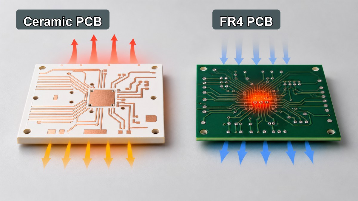
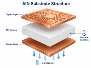
For PCB buyers, the term is often used when comparing ceramic PCB substrates with FR4, metal core PCB and aluminum nitride ceramic. Alumina is not a metal heat spreader, but it conducts heat much better than ordinary organic PCB laminates while maintaining electrical isolation. This makes it useful where a circuit needs both insulation and a shorter heat path.
What Is the Typical Thermal Conductivity of Alumina?
Typical dense alumina ceramic used for electronics substrates is often specified around 20-30 W/m·K, while very dense or high-purity alumina grades may be listed higher by some material suppliers. The exact value should always be taken from the ceramic supplier’s data sheet because purity, porosity, grain structure and processing route can change the result.
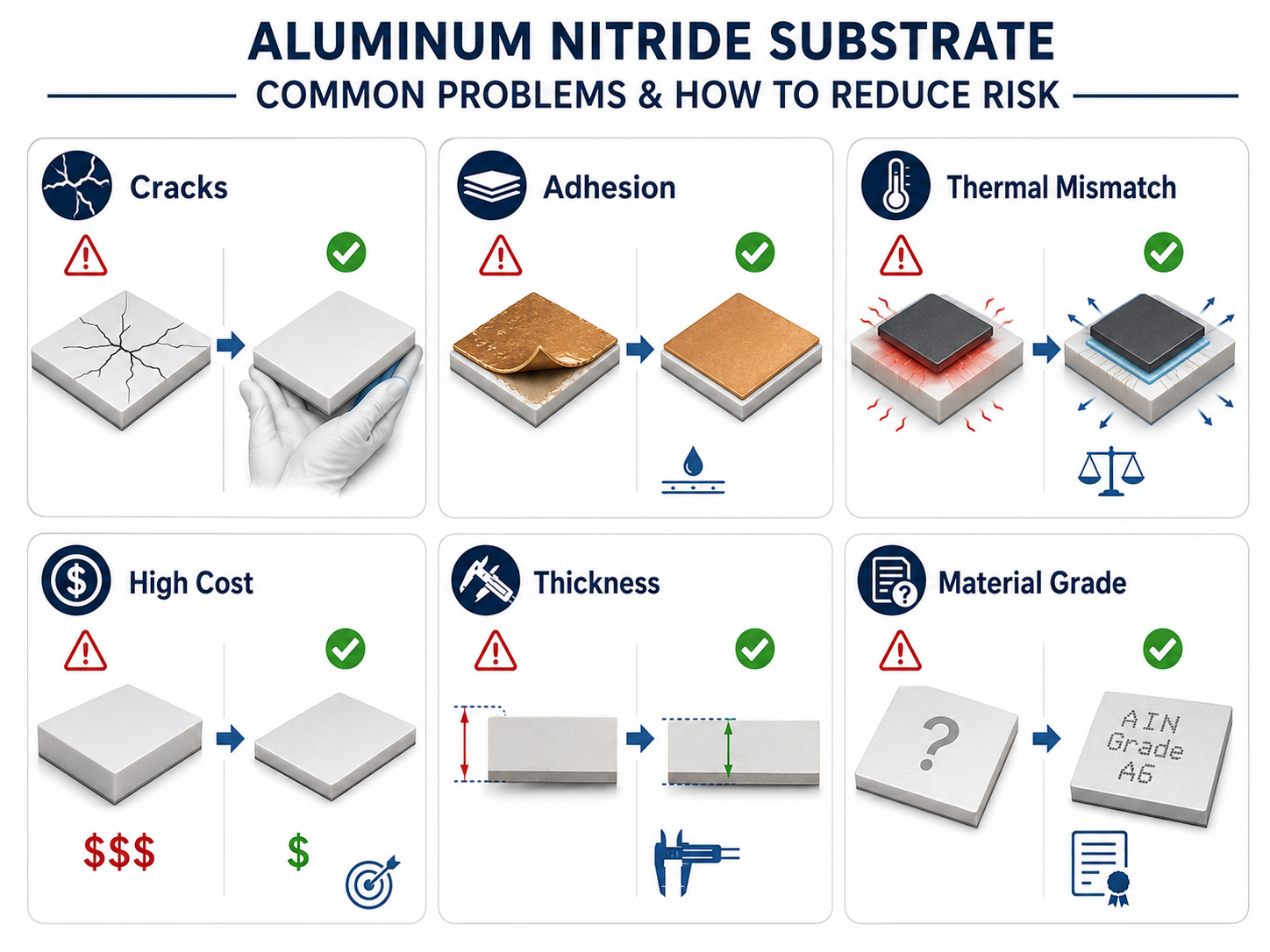
For practical ceramic PCB selection, it is safer to treat alumina as a balanced thermal-insulating material rather than a maximum-conductivity material. If a design only needs moderate heat spreading, alumina can be a cost-effective choice. If the component has very high heat flux, AlN or another high-thermal-conductivity substrate may need review.
Is Alumina Conductive or Electrically Insulating?
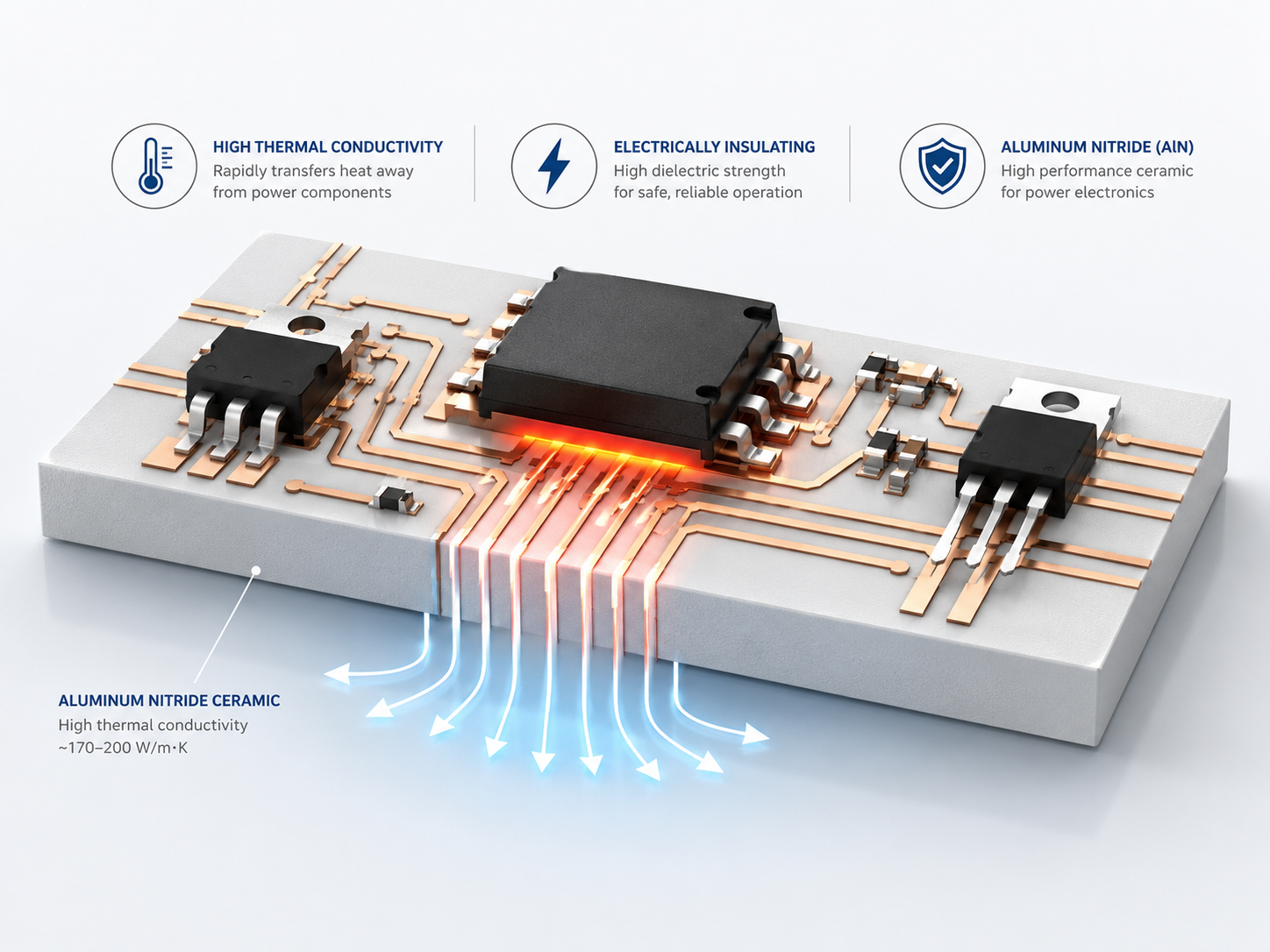
Alumina is thermally conductive compared with FR4, but it is electrically insulating under normal electronics operating conditions. This distinction matters because many searches for “alumina conductivity” mix thermal conductivity and electrical conductivity into one phrase.
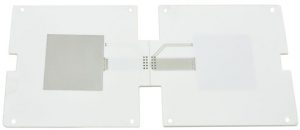
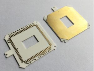
In PCB use, the value of alumina is that heat can pass through the ceramic while voltage isolation is maintained between copper features, components and the heat sink. This is why alumina ceramic substrates are used in LED modules, sensor circuits, power resistors, hybrid circuits, automotive electronics and other designs where heat and insulation must be handled together.
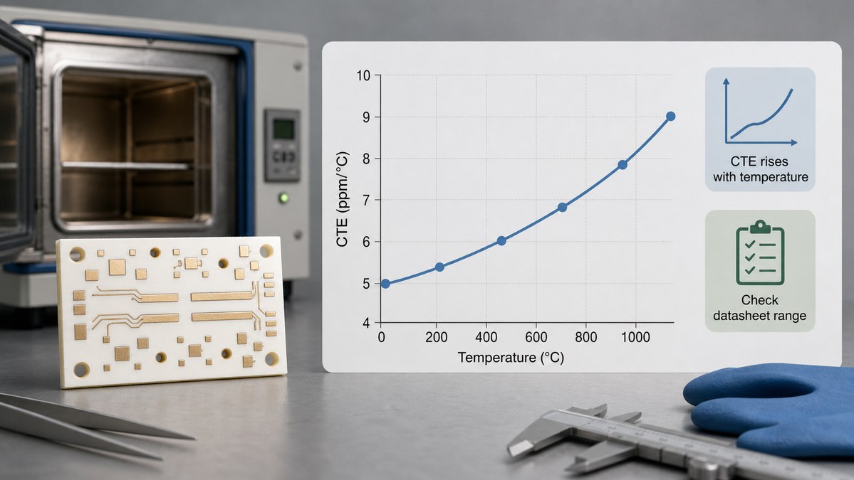
How Does Alumina Thermal Conductivity Change with Temperature?
Alumina thermal conductivity generally decreases as temperature rises because phonon scattering increases inside the ceramic. Published research and material databases show that temperature-dependent values can vary significantly by sample type, density and measurement method.
For PCB design, this means a room-temperature conductivity value should not be used blindly for high-temperature operation. If the board will operate near a hot device, inside an enclosed module or under repeated thermal cycling, request temperature-dependent material data and validate the full stack under the expected operating range.
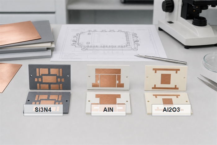
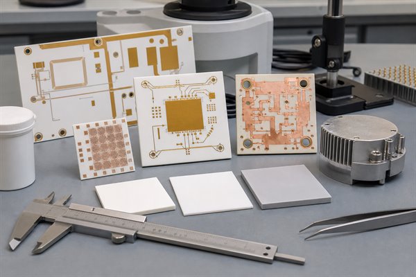
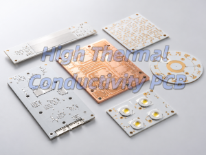
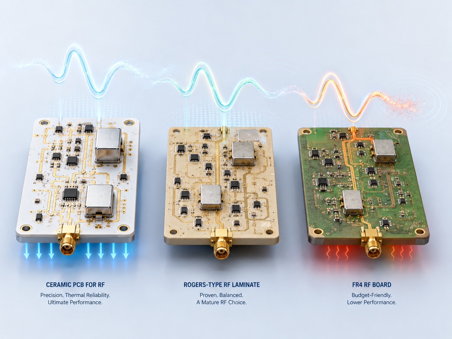
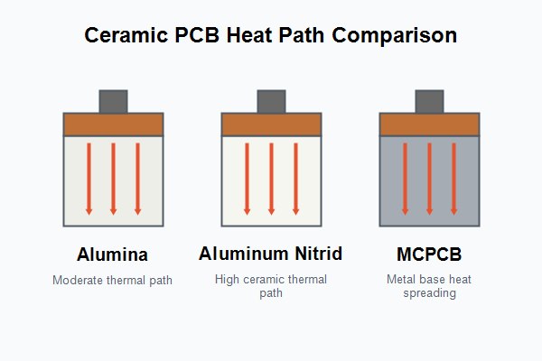
How Do Alumina, FR4, MCPCB and AlN Compare?
The useful comparison is not “which material has the highest heat conductivity” in isolation. The better question is which material gives enough heat transfer, insulation, reliability and manufacturability for the assembly.
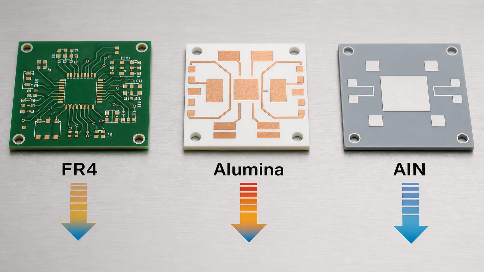
| Material | Typical Thermal Role | Electrical Behavior | Best Fit |
|---|---|---|---|
| FR4 | Low thermal conductivity | Insulating laminate | Standard control circuits, signal boards and low-heat designs |
| MCPCB | Uses a metal base and dielectric layer for heat spreading | Dielectric layer provides isolation | LED lighting, power boards and cost-sensitive thermal designs |
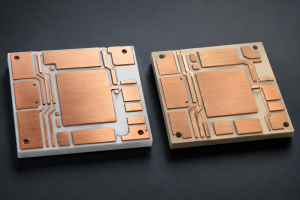
| Alumina ceramic PCB | Moderate-to-good ceramic thermal conductivity | Electrical insulator | Insulated ceramic circuits needing stable cost, hardness and heat transfer |
| AlN ceramic PCB | High ceramic thermal conductivity | Electrical insulator | High heat flux, compact power modules, laser drivers and demanding thermal paths |
If the design is mainly limited by FR4’s poor heat transfer, alumina may be enough. If the design is limited by junction temperature in a compact high-power package, compare alumina with high thermal conductivity ceramic PCB options such as AlN.
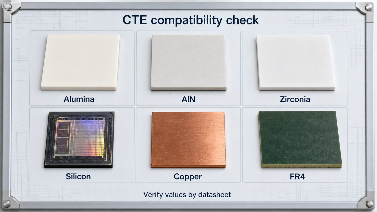
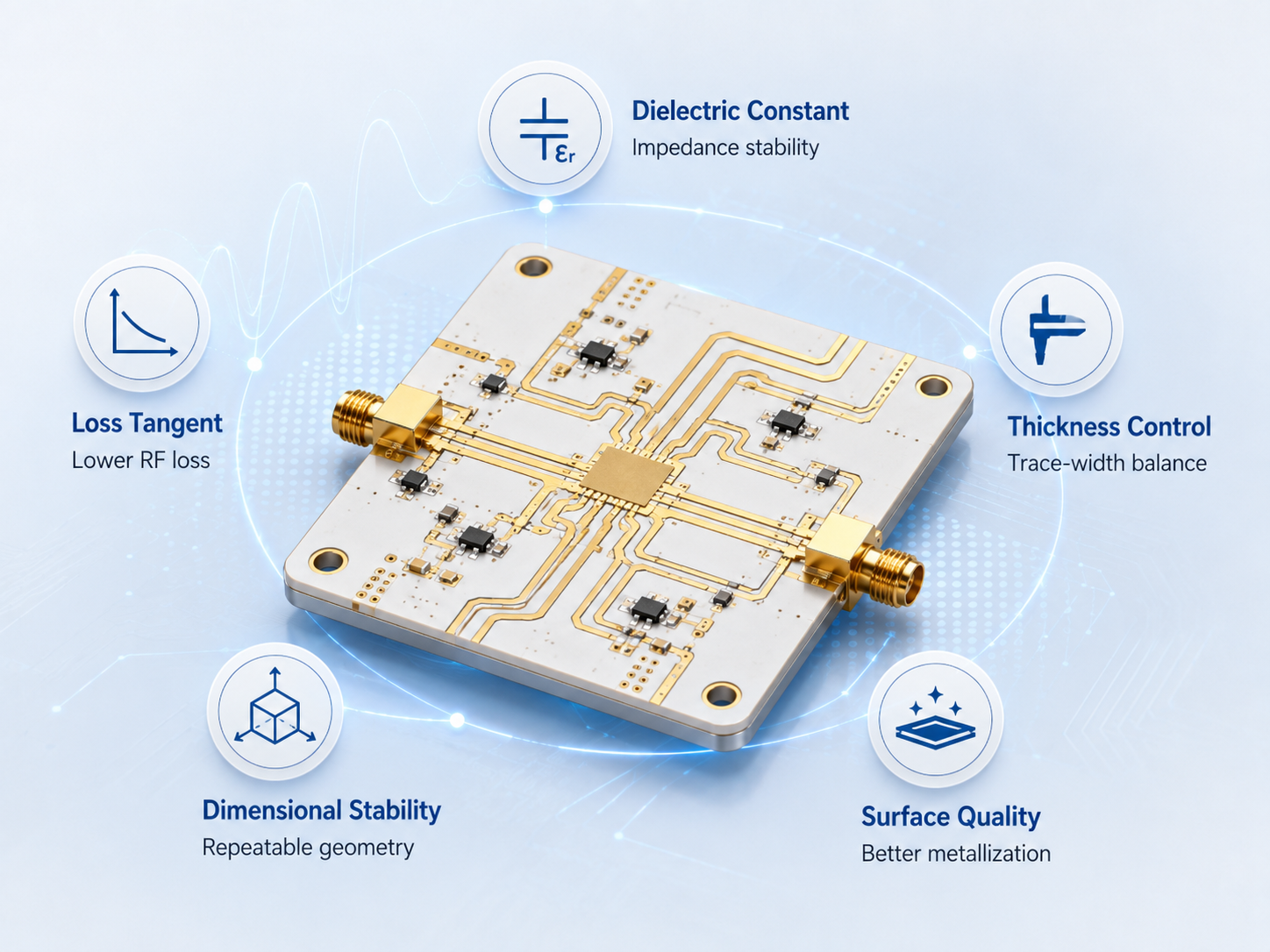
Which Alumina Properties Matter Besides Heat Conductivity?
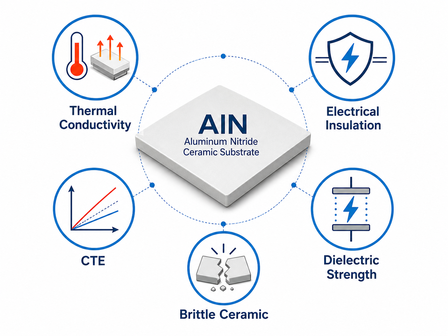
Alumina properties should be reviewed as a package, not as a single thermal number. Heat conductivity is important, but density, specific heat capacity, hardness, dielectric strength, CTE, surface roughness and flatness can all affect PCB performance and assembly reliability.
- Density: Higher density usually means fewer pores and more stable mechanical and thermal behavior.
- Specific heat capacity: This affects how much heat the ceramic can absorb before its temperature rises.
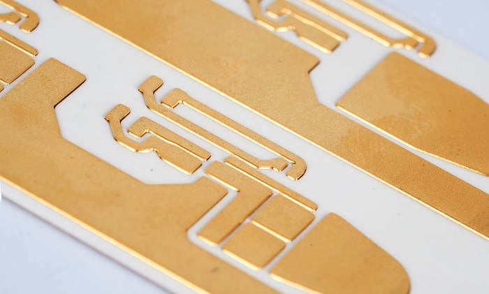
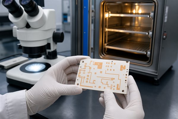
- Hardness: Alumina is hard and wear-resistant, but machining, laser cutting and drilling require ceramic-capable processes.
- CTE: Thermal expansion affects copper stress, solder fatigue and compatibility with components.
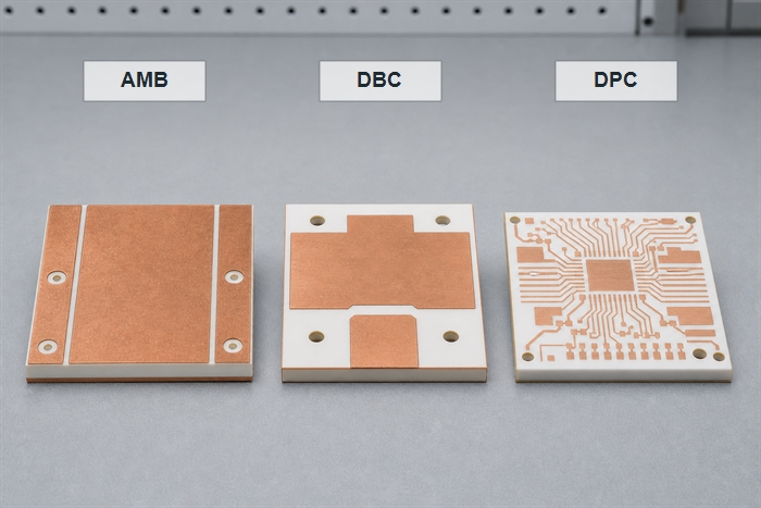
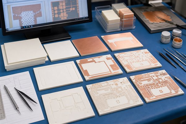
- Surface quality: Thin film, thick film, DPC and DBC processes may require different surface conditions.
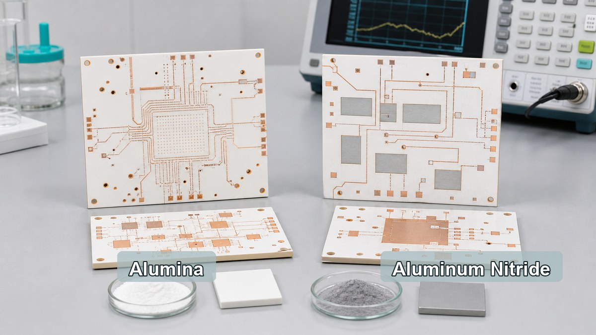
For sourcing, ask whether the quoted value is for 96% alumina, 99.6% alumina or another grade. A higher-purity material may support better surface quality or stability, but it may not automatically solve every thermal or cost problem.
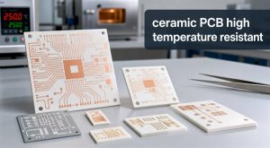
When Is Alumina Ceramic PCB a Good Choice?
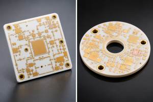
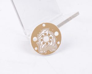
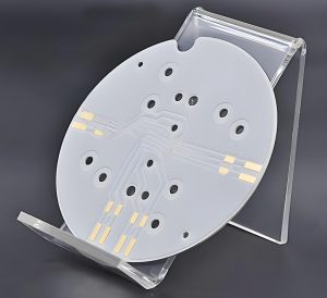
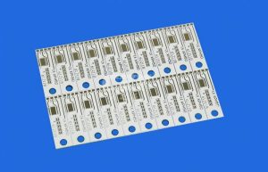
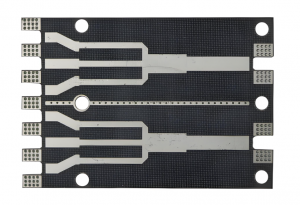
Alumina ceramic PCB is a good choice when the design needs better heat transfer than FR4, strong electrical insulation, good mechanical strength and a more cost-accessible ceramic option than AlN. It is often practical for medium-power modules, LED substrates, sensor electronics, thick-film circuits, precision resistive circuits and industrial control boards.
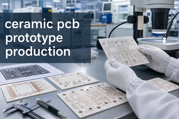
Alumina also fits projects where production availability and process maturity matter. EBest Circuit (Best Technology) supports ceramic PCB projects including alumina and AlN options, and engineering review can help determine whether ceramic substrate selection, copper thickness and surface finish match the operating conditions.
When Is Alumina Not Enough for Thermal Management?
Alumina may not be enough when the heat source is very small, the power density is high, the board has limited copper area, or the assembly has a weak interface to the heat sink. In those cases, upgrading the substrate alone may not fix the thermal bottleneck unless the full stack is redesigned.
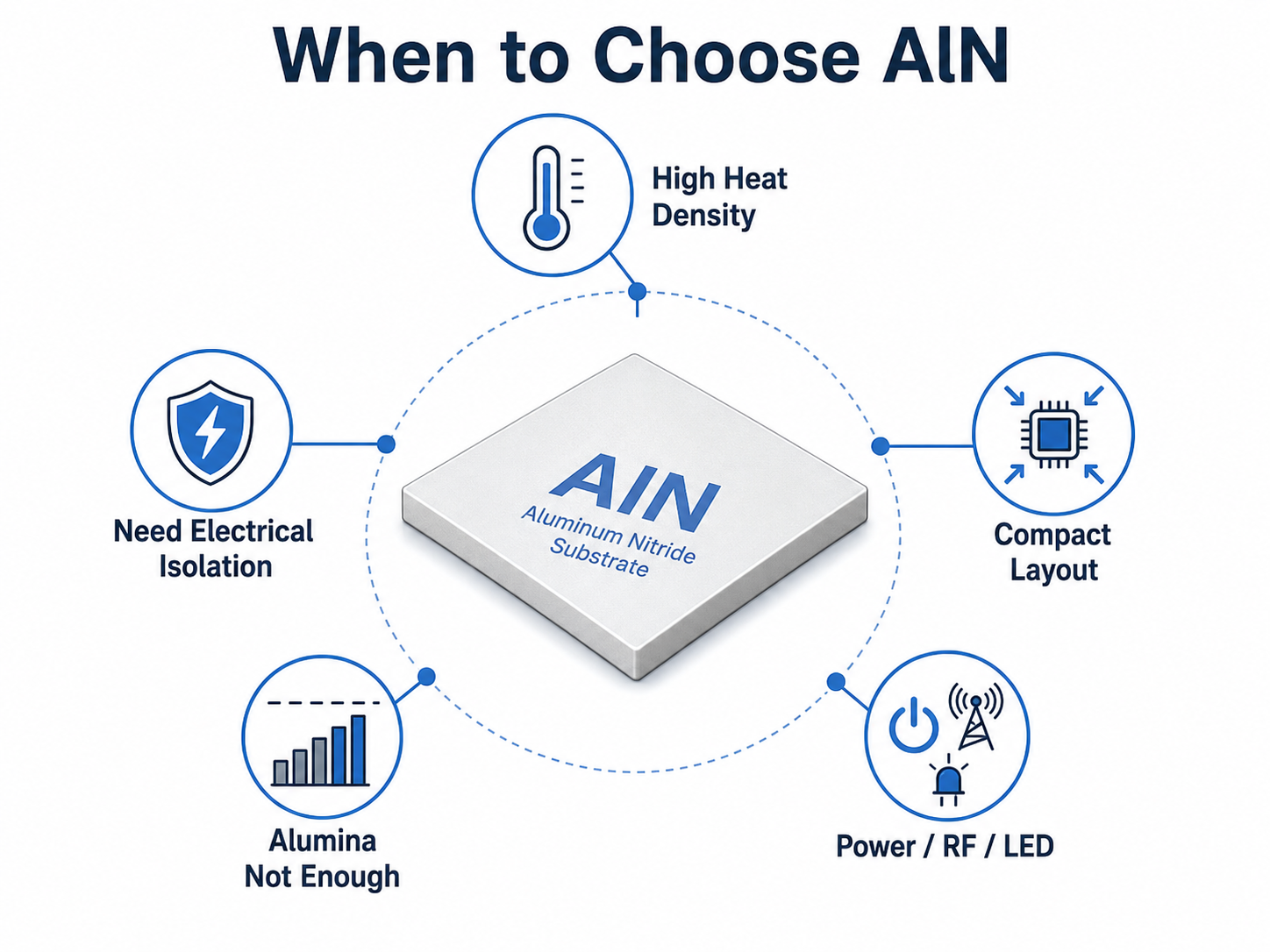
AlN should be considered when thermal conductivity is the controlling requirement and the project can justify the higher material and processing cost. BeO has high thermal conductivity, but its toxicity and handling restrictions make it unsuitable for many commercial PCB programs. For cost-sensitive ceramic designs, review whether a cost-effective Al2O3 ceramic PCB approach can meet the thermal target before moving to a higher-cost material.
How Do Thickness, Copper Area and Interfaces Change Heat Transfer?
Thermal conductivity is a material property, while heat transfer in a PCB assembly depends on geometry and interfaces. A thinner alumina substrate can reduce through-thickness thermal resistance, but it may reduce mechanical margin. Larger copper areas can spread heat, but copper imbalance may increase stress and warpage.
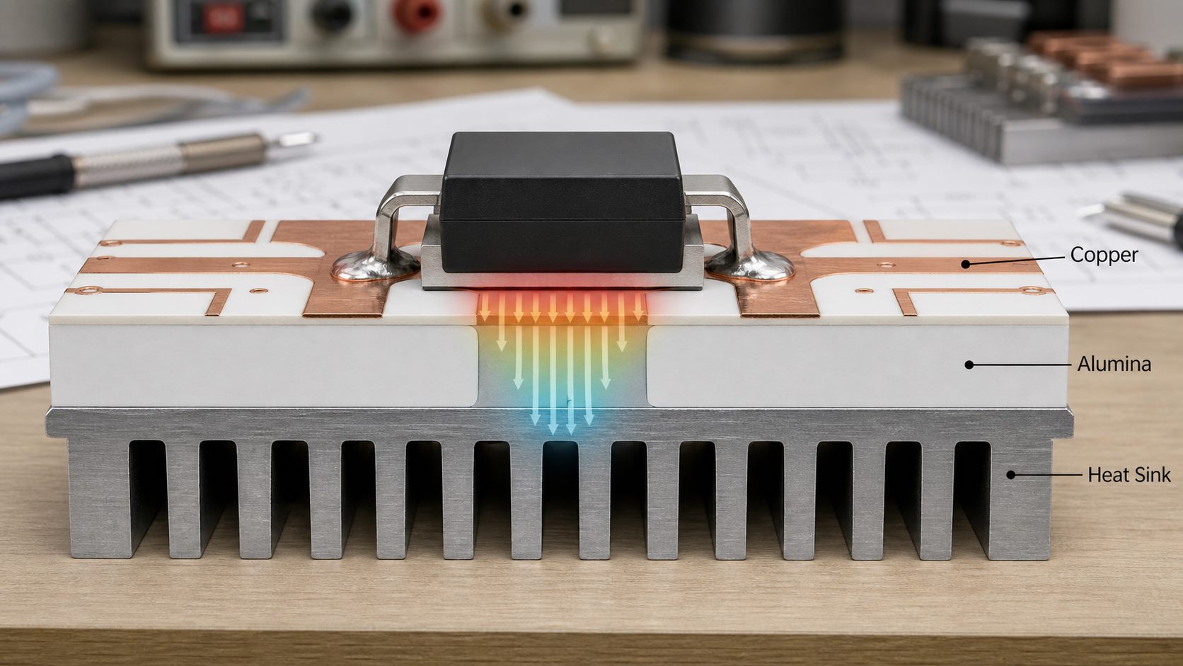
The interface between the ceramic board and heat sink is often as important as the ceramic itself. Gaps, poor flatness, insufficient mounting pressure or unsuitable thermal interface material can cancel part of the benefit gained from a better substrate. A useful thermal review should include component footprint, copper layout, ceramic thickness, surface finish, mounting method and cooling structure.
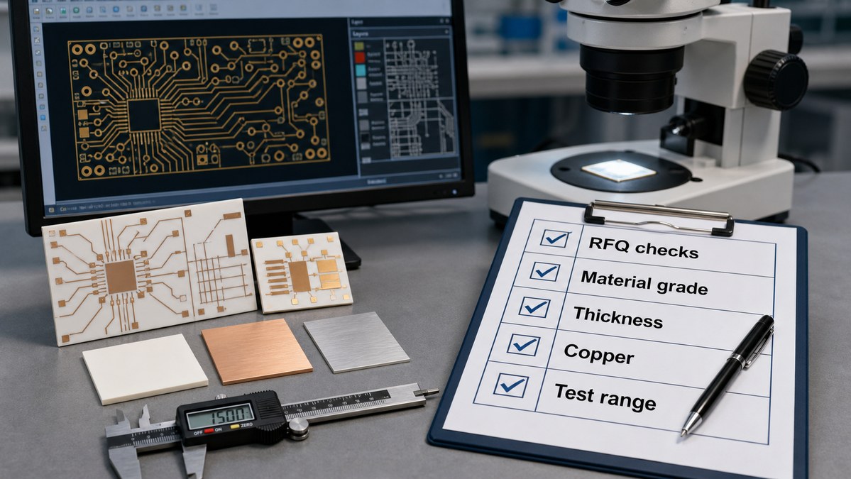
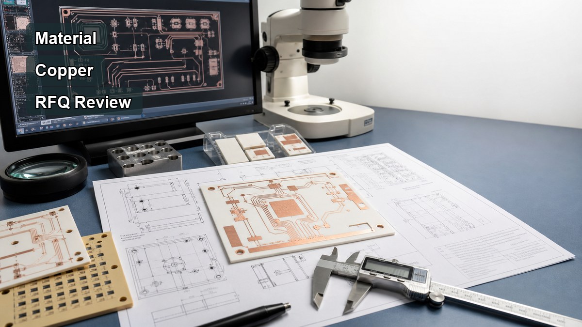
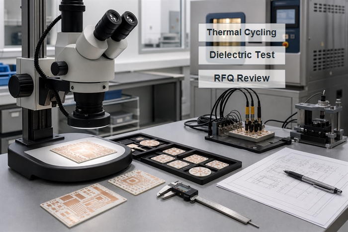
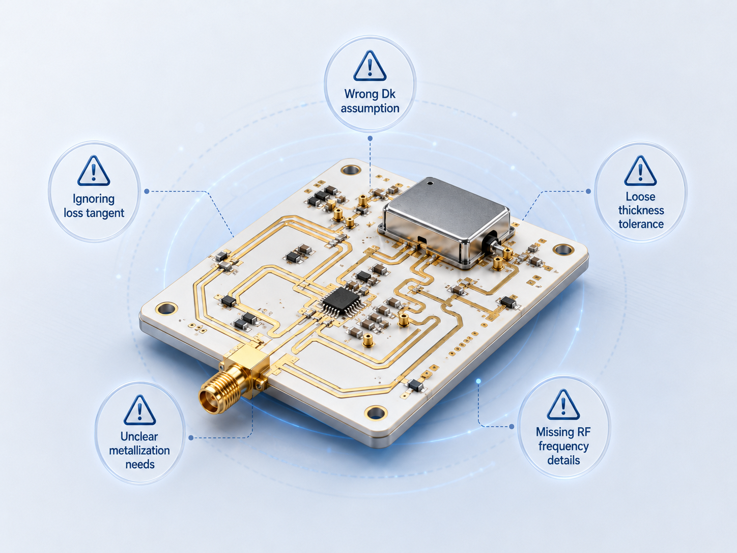
What Should Buyers Provide for an Alumina Ceramic PCB RFQ?
An alumina ceramic PCB RFQ should provide enough technical data to judge thermal path, manufacturability and reliability. A request that only says “need alumina PCB” is usually too vague for accurate quotation or process advice.
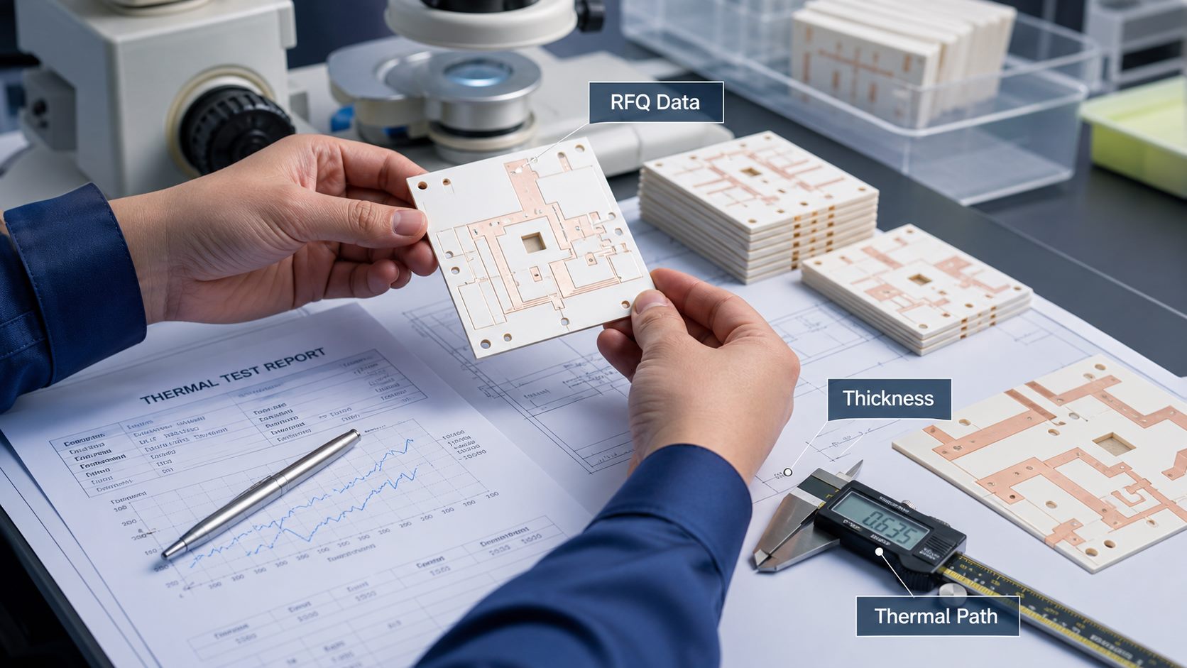
- Target alumina grade, such as 96% or 99.6%, or permission for supplier recommendation.
- Ceramic thickness, outline size, holes, slots and tolerance requirements.
- Copper thickness, minimum line and spacing, copper balance and surface finish.
- Expected heat source size, power dissipation, operating temperature and cooling method.
- Electrical insulation requirement, voltage clearance and dielectric test expectations.
- Manufacturing route preference: thick film, thin film, DPC, DBC or open for review.
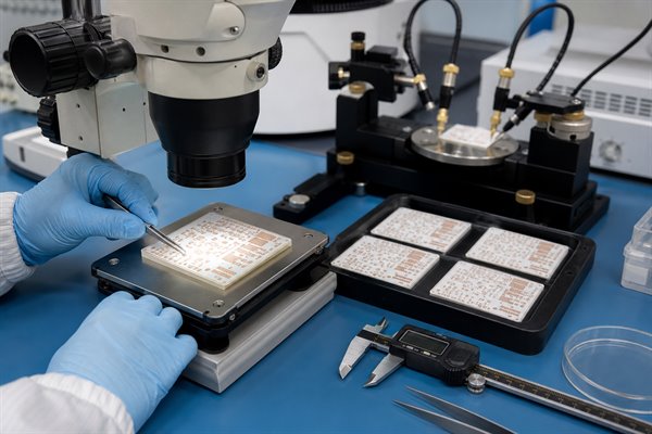
- Prototype quantity, annual volume, inspection requirements and assembly method.
For projects that also require component mounting, BOM review or testing, EBest Circuit can review PCB fabrication and PCBA needs together. Send drawings, stack-up notes, thermal assumptions and quantity targets to contact EBest Circuit or email sales@bestpcbs.com.
FAQ About Alumina Heat Conductivity?
1. What is heat conductivity?
Heat conductivity, usually called thermal conductivity in engineering, is a material’s ability to conduct heat. It is measured in W/m·K and helps compare how quickly heat can pass through different materials.
2. Is alumina a good conductor of heat?
Alumina is a good heat conductor compared with FR4 and many insulating polymers, but it is not as conductive as metals or aluminum nitride ceramic. It is best viewed as an electrically insulating ceramic with useful thermal performance.
3. Is alumina electrically conductive?
No. Alumina is normally used as an electrical insulator in PCB and electronic packaging applications. Its value is that it can transfer heat while helping maintain electrical isolation.
4. What material has the highest heat conductivity for ceramic PCBs?
Among common ceramic PCB materials, BeO has very high thermal conductivity but serious handling restrictions. AlN is a more common high-conductivity ceramic choice for electronics, while alumina is chosen for balanced cost, availability and insulation.
5. Does alumina thermal conductivity change with temperature?
Yes. Alumina thermal conductivity generally decreases as temperature rises, so high-temperature designs should use temperature-dependent data rather than relying only on a room-temperature number.
6. Is alumina hazardous?
Finished alumina ceramic substrates are generally stable in normal use, but ceramic dust from machining or grinding should be controlled with proper industrial safety practices. Buyers should request material and process compliance information when needed.
Conclusion
Alumina heat conductivity is useful because it gives PCB designers a thermally capable ceramic substrate while preserving electrical insulation and mechanical stability. The important decision is not only the W/m·K value. Ceramic grade, thickness, copper layout, interface material, heat sink design, temperature range and production process all affect the final thermal result.
If you are evaluating alumina ceramic PCB, AlN ceramic PCB or a mixed PCB/PCBA build, EBest Circuit (Best Technology) can review your drawings, thermal assumptions, process route and quotation files. For engineering review or quotation, contact sales@bestpcbs.com.