





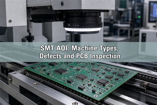
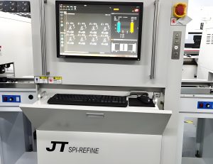
SMT AOI uses automated optical inspection to check visible components and solder joints during surface-mount assembly. An SMT AOI machine can flag missing parts, incorrect orientation, placement offsets and visible solder defects. It does not prove that every connection is electrically sound, and it cannot see through a package to inspect hidden solder joints. Its value comes from combining repeatable visual checks with a defined defect-review process.
What Is AOI in SMT?
AOI is an optical inspection step, not a component-placement process. The AOI full form is automated optical inspection; SMT means surface mount technology. Together, the SMT AOI full form describes automated optical inspection used in a surface-mount production process.
The practical SMT AOI meaning is straightforward: compare the visible assembly with approved component, position and solder criteria, then route suspect locations for review. A camera image alone is not a pass/fail standard. The program must know which parts should be present, their polarity, and the allowed variation for the assembly.
How Does an SMT AOI Machine Work?
An AOI machine for PCB assembly captures controlled images, aligns them with the board data, and evaluates selected features. A typical inspection cycle has five steps:
- Load and identify: select the correct board revision and inspection program.
- Align: locate fiducials so inspection windows match the physical components.
- Capture: use suitable lighting and camera views; a 3D system also measures surface height.
- Evaluate: compare placement, markings and visible joint features with validated limits.
- Review: confirm flagged defects, record the decision, and send affected boards for controlled repair or disposition.
SMT AOI inspection can use design data, component libraries and reference images. Reference boards must themselves be checked: copying a defective sample into the library can teach the system to accept the same defect again.
Where Does AOI Fit in the SMT Process?
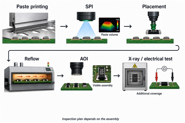
The SMT AOI process is commonly placed after component placement or after reflow, with a different inspection objective at each position. Pre-reflow inspection checks placement before solder joints form. Post-reflow inspection checks the resulting visible assembly and exposed solder connections.
A typical SMT machine process is paste printing, solder paste inspection (SPI), placement, reflow and post-reflow AOI. An additional pre-reflow station may be useful when early placement feedback justifies the extra step. SMT line AOI should be positioned around the defects that need to be contained, rather than treated as a substitute for every other test.
Upstream control matters. The SMT stencil influences where paste is deposited and how much paste reaches each pad. SPI can identify an abnormal deposit before placement, whereas post-reflow AOI sees the visible result after soldering.
SMT AOI Defects List: What Can It Detect?
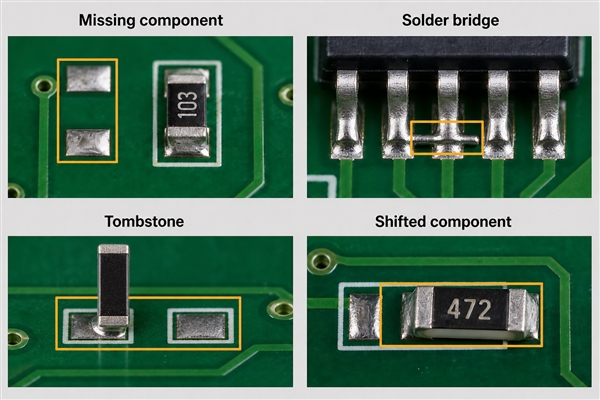
Common SMT AOI defects include missing or displaced components, visible polarity errors, tombstoning and exposed solder bridges. Detection depends on optical access, resolution, the inspection program and the actual package.
| Defect | Visible inspection feature | Important limitation |
|---|---|---|
| Missing component | Expected body or termination is absent | Intentional do-not-populate positions must be programmed correctly |
| Placement offset or rotation | Body and leads differ from the approved position | Acceptance depends on the footprint and applicable assembly criteria |
| Incorrect polarity | Visible stripe, dot or marking has the wrong orientation | An unmarked or obscured part cannot be identified reliably from that feature |
| Tombstone or lifted lead | One end stands up or an exposed lead is elevated | View angle and height measurement affect coverage |
| Solder bridge | Visible solder joins adjacent leads or pads | Bridges under a package need another inspection method |
| Insufficient or excessive solder | Exposed fillet shape or measured surface differs from limits | Appearance alone does not establish joint strength or internal integrity |
| Wrong component | Package or readable marking differs from the library | Same-size unmarked parts can be electrically different |
The following illustration shows representative visual defects, not production inspection records. A suspected cold joint, internal void or hidden open must not be declared confirmed solely from its appearance in an ordinary AOI image.
What Is the Difference Between 2D and 3D AOI?
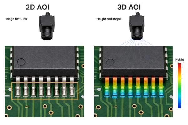
2D AOI evaluates image features such as shape, color, contrast and markings. 3D AOI adds measured height and surface geometry. That additional information helps distinguish a raised lead or abnormal component height from a harmless change in brightness.
SMT 3D AOI is particularly useful when coplanarity and exposed solder shape matter. It still needs a visible measurement path: tall components can obstruct views, shiny solder can create reflections, and package bodies hide underside connections. More dimensions do not remove those physical constraints.
Modern AOI machines often combine 2D identification with 3D measurement rather than discard one for the other. Multi-direction imaging and reflection control are model-dependent capabilities, not a universal guarantee for every board.
AOI vs SPI, X-Ray and Electrical Testing
These methods inspect different evidence. An SMT SPI AOI comparison starts with paste deposits versus assembled components; X-ray adds access to some hidden structures, while electrical tests check selected circuit behavior.
| Method | Main target | What a pass does not prove |
|---|---|---|
| SPI | Paste height, area, volume and offset before placement | That reflow will form acceptable joints |
| AOI | Visible placement, orientation and solder features | Hidden-joint integrity or correct electrical function |
| X-ray / AXI | Internal solder structures accessible to the selected imaging method | Every electrical failure or long-term reliability mechanism |
| ICT or flying probe | Accessible nets and component parameters within the test coverage | Untested nodes or complete operation under all conditions |
| Functional test | Defined operating behavior and interfaces | Every latent defect or cosmetic assembly requirement |
The term AOI testing is often used informally, but optical inspection is not an electrical continuity test. A board can pass visual inspection and still contain an incorrect unmarked resistor, programming error or hidden connection fault. The inspection plan must state how those remaining risks are covered.
What Does SMT AOI Programming Involve?
SMT AOI programming turns the approved assembly definition into repeatable inspection windows and decision limits. Start with the current board revision, reference designators, placement coordinates, component orientation and populated/unpopulated positions.
- Match the board origin, fiducials and panel array to the manufacturing data.
- Select component-library entries that match actual package dimensions and visible markings.
- Set lighting, views and height ranges for the inspected features.
- Validate with independently accepted boards and known defect examples.
- Record the program revision and revalidate changes to packages, layout or acceptance limits.
Do not widen limits simply until every sample passes. A valid change should preserve defect detection while accommodating legitimate process variation. IPC acceptance requirements, where specified, must be translated using the agreed standard revision, product class and customer criteria; a machine label alone does not establish compliance.
How Are AOI False Calls and Escapes Controlled?
A false call flags an acceptable assembly; an escape is a defect that inspection misses. Reducing one by blindly relaxing thresholds can worsen the other. Review both against independently verified samples.
The SMT AOI operator checks flagged locations, separates genuine defects from image artifacts, and escalates recurring patterns. Engineers then investigate the specific cause: poor fiducial recognition, board movement, package-library mismatch, reflective surfaces or unstable solder geometry.
Keep image evidence, defect location, program revision and review outcome together. Track rates with consistent denominators: calls per board and defects per inspected joint are not interchangeable. Measurement results and verified defect trends can guide process adjustments, but they do not justify a blanket zero-defect promise.
How Do PCB Layout and Panel Support Affect AOI?
AOI needs stable positioning and a usable line of sight. On an FR4 PCB, board bow, inadequate support and obstructed fiducials can move features away from their expected inspection locations. Tall connectors beside small joints may restrict side-camera views.
Keep fiducials clear and consistent, provide legible polarity markings, and confirm that the assembled board fits the machine’s clearance and support arrangement. Check visibility around tall parts before freezing placement. There is no single clearance value that works for every camera system and component combination.
For arrays, the PCB panelization layout must match the programmed repeat positions. Rails, tooling and support should hold the panel without obstructing the areas to inspect. A locally shifted sub-board can create repeated false calls even when the global panel origin is correct.
What Affects SMT AOI Machine Price and Line Fit?
SMT AOI machine price varies with measurement technology, optical resolution, board size, conveyor configuration, software and support. A standalone price without its configuration does not describe inspection capability.
An SMT inline AOI machine connects to production conveyors for routine flow; an SMT AOI offline machine can inspect separately from the line. Actual cycle time includes loading, alignment, scanning, analysis and board transfer. It must be evaluated on the intended assembly, not inferred from a camera-speed figure.
AOI machine brand is only one factor. Yamaha SMT AOI products, for example, include the YRi-V family; other manufacturers offer different imaging and programming approaches. Compare the specified model and its verified board coverage, not a brand name alone. Used SMT AOI equipment also needs checks for calibration, software licensing, component-library compatibility and support availability.
AOI PCB inspection price is a different question from buying equipment: the inspection cost within assembly depends on program preparation, board complexity, cycle time and review effort. We provide PCB manufacturing and assembly services, with inspection matched to each assembly’s requirements.
How Does BestPCBs Use AOI in PCB Assembly?
At EBest Circuit (Best Technology), we integrate optical inspection into our PCB assembly workflow alongside complementary checks. Our inspection equipment includes a SINIC-TEK A510DL 3D AOI system, a SINIC-TEK S8080 3D SPI system and UNICOMP AX8200 X-ray equipment.
Our assembly capabilities include SMD components down to 01005 and BGA pitch down to 0.25mm, subject to engineering review for the actual design. These limits do not mean that every such package can be completely inspected optically. We tailor the inspection plan to package visibility, assembly requirements and the agreed electrical or functional tests.
SMT AOI Questions and Answers
What Is AOI Machine?
It is camera-based equipment that inspects visible assembly features against a programmed reference. It flags suspect locations for review; it does not repair them.
What Is SMT Machine?
The term describes equipment used in surface-mount manufacturing, including printers, placement machines and inspection systems. A placement machine mounts components; AOI checks selected visible features.
What Is SMT Machine Operator?
This is a production role operating the assigned SMT equipment. An SMT AOI machine operator specifically runs inspection programs and reviews flagged results according to the approved procedure. Program validation and acceptance-limit changes need the designated engineering authority.
Can AOI Inspect BGA Solder Joints?
It can inspect the visible package body and relevant external features, but the underside ball array is hidden. X-ray and appropriately designed electrical tests provide additional coverage; their own limitations still need evaluation.
Conclusion
Effective SMT AOI combines suitable optics, validated programming, stable board handling and disciplined defect review. It works best as part of an inspection plan that also addresses paste quality, hidden connections and electrical function. To discuss your PCB assembly requirements with our team, contact sales@bestpcbs.com.
You may also like




Tags: 3D AOI, automated optical inspection, PCB Assembly, SMT AOI, SMT AOI machine, solder inspection