A Castellated PCB is a module board with plated holes cut through its edge so the remaining half-holes can be soldered directly to matching pads on a carrier board. A reliable result depends on four connected decisions: the module edge must be manufacturable, the carrier footprint must support a controlled solder joint, the assembly process must limit movement and solder loss, and inspection must confirm both the plated edge and the completed joint.
This guide is written for hardware designers, manufacturing engineers, quality teams, and sourcing teams who need to release a castellated module without treating the edge connection as an ordinary row of vias. It explains what to specify in fabrication data, what to check during assembly, which defects change electrical or mechanical performance, and what evidence should accompany a production order.
Before requesting a fabrication and assembly review, prepare the proposed stackup, Gerber or ODB++ data, NC drill file, module drawing, carrier-board footprint, quantity, and inspection requirements. EBest Circuit can use those inputs to identify open manufacturability questions before pricing.

What Must Be Confirmed Before Manufacturing a Castellated PCB?
A Castellated PCB release should proceed only after the board-edge geometry, finished-hole intent, surface finish, panel support, carrier footprint, and acceptance evidence are specified together. These inputs are linked: changing the routed outline changes the remaining half-hole, which changes the carrier-pad overlap, solder volume, and visible inspection result.
The following release map separates design intent from factory interpretation and shows which record should close each decision.
| Release Input | Decision Required | Risk if Undefined | Approval Record |
| Board outline and drill data | Confirm which plated holes the routed edge intersects and how much hole remains | Uneven half-holes, exposed substrate, or an edge that misses the plated barrel | CAM image or marked fabrication drawing |
| Pad and annular-ring geometry | Preserve enough copper on the outer layers and required inner layers after routing | Weak edge plating, copper breakout, or local delamination during depanelization | ODB++ or Gerber review plus stackup |
| Surface finish | Choose a finish compatible with the edge geometry, storage plan, and soldering process | Poor wetting, excessive thickness variation, or finish damage at the routed edge | Purchase specification and supplier confirmation |
| Panel and break-tab plan | Keep tabs, rails, and tooling features away from functional castellated edges | Burrs, crushed plating, module distortion, or uncontrolled manual rework | Approved panel drawing |
| Carrier-board land pattern | Match module pitch, body outline, solder fillet space, and placement tolerance | Open joints, bridging, module rotation, or insufficient visible fillet | Footprint drawing and assembly review |
A quotation should state which inputs remain provisional. If the factory must choose the finished hole, remaining-hole ratio, panel-tab position, or carrier-pad extension, those decisions belong in the engineering-question record rather than being inferred silently during CAM.
How Are Castellated Half-Holes Formed and Finished?
Castellated PCB half-holes are normally produced by plating complete drilled holes first and routing the final board outline through those plated barrels afterward. The sequence matters because drilling, copper deposition, surface finish, routing, cleaning, and inspection each affect a different part of the remaining edge.
Step 1: Register the drill and outline. CAM must confirm that the finished outline intersects the intended plated-hole centers within the supplier’s routing and registration capability. The check uses the released drill file, outline layer, fabrication drawing, and the supplier’s documented tolerance; an offset cut can leave too little barrel or too much protruding copper.
Step 2: Plate the complete hole. The drilled barrel receives the same hole-wall preparation and copper-plating controls required by the applicable board construction. Copper continuity should be evaluated before routing because the cut edge cannot restore a thin, voided, or poorly bonded barrel.
Step 3: Apply the specified surface finish. The purchase data must name the finish and any thickness or storage requirements that matter to assembly. Finish selection is order-specific; one supplier’s published minimum hole or preferred finish should not be treated as a universal design rule.
Step 4: Route through the plated barrels. A suitable tool, feed strategy, support method, and cut direction are selected to limit copper tearing, resin smear, and edge burrs. The factory should verify the routed sample at magnification before the lot proceeds when the geometry is new or near its process boundary.
Step 5: Clean and inspect the edge. Loose copper, laminate debris, plating stubs, and conductive particles must be removed without thinning the usable barrel. Final inspection compares the remaining copper, edge condition, pitch, and board dimensions with the approved drawing and acceptance plan.
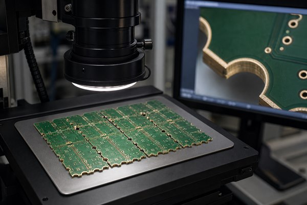
The manufacturing sequence above is consistent with Eurocircuits’ published explanation of plating complete holes before routing through the barrels. Its published dimensions are useful examples of one supplier’s process, but the order must use the capability statement of the factory that will build the board.
Which Board-Edge Details Control Castellated Hole Quality?
Castellated PCB edge quality is controlled by the routed split position, copper retained around the barrel, solder-mask clearance, local laminate support, and distance from panel tabs. These features determine whether routing leaves a stable plated semicircle or a damaged copper shell with little mechanical support.
This relationship applies only when the routed outline passes through the finished-hole centerline. Drill registration, routing registration, tool runout, copper condition, and the supplier’s finished-edge tolerance still determine the acceptable production window.
- Split position: Show the finished edge through the intended hole location and obtain a CAM image of the resulting half-hole. A centerline assumption is not enough when routing and drill registration consume a large share of the remaining copper.
- Copper retention: Specify outer-layer pads and any required inner-layer support so that routing does not remove the copper needed to anchor the barrel. The acceptable geometry must come from the chosen supplier’s stackup and capability review.
- Solder-mask opening: Keep mask from covering the area intended to wet, but avoid unnecessary exposed copper that can collect excess solder or reduce spacing to adjacent nets. Review the actual mask swell used in CAM.
- Edge clearance: Keep unrelated traces, planes, components, and mechanical features outside the supplier’s routed-edge clearance. An exposed plane or trace at the cut edge can create corrosion, shorting, or handling risk.
- Tab separation: Reserve nonfunctional edge length for panel support. A mouse bite or break tab across a functional plated half-hole can tear copper and make the final module dependent on manual filing.
Prototype data should also identify intentional full holes, slots, or header pads near the castellations. These features can change paste flow and local copper balance, so the supplier must distinguish them from the plated holes intended to be routed.
How Should a Carrier PCB Footprint Support a Castellated Module?
A Castellated PCB carrier footprint must give every half-hole a matching pad, enough exposed copper for a controlled fillet, and a body outline that prevents placement ambiguity. The module drawing and carrier land pattern should be approved as a pair because module pitch tolerance, routed-edge tolerance, and placement tolerance accumulate at the outer joints.
- Pad alignment: Center each carrier pad on the nominal castellated feature and verify the worst-case overlap at both ends of the row. Do not correct pitch mismatch by enlarging pads until adjacent-net spacing becomes marginal.
- Fillet extension: Extend the carrier pad beyond the module edge only as much as required for solder deposition, wetting, and visible inspection. The amount should be validated with the stencil and reflow process rather than copied from an unrelated module.
- Body clearance: Keep components, test points, and copper features clear of the module body, underside terminations, and any permitted overhang. Include courtyard space for placement tooling and optical inspection.
- Assembly datum: Add a clear outline, polarity or pin-one mark, and usable fiducials so the placement program does not rely only on the castellated row. Confirm that the module can be held flat during reflow.
- Rework access: Preserve probe and soldering access to the edge joints when field repair or engineering rework is expected. Dense neighboring parts can make a nominally visible joint impossible to inspect or touch up.
Before release, place the module footprint over the supplier’s maximum board outline and half-hole envelope. This worst-case overlay reveals end-pad loss, courtyard conflicts, and solder-mask spacing problems that a nominal 3D rendering can hide.
How Should Castellated PCB Modules Be Assembled?
A Castellated PCB module can be assembled as a surface-mount part only when paste deposition, placement support, reflow history, and joint visibility have been specified for that module and carrier board. The process should control both electrical wetting and the module’s final height, rotation, and coplanarity.
Step 1: Confirm the received module condition. Inspect the routed edges for loose plating, oxidation, contamination, bent boards, and dimensional damage before paste printing. Record the lot and sample results so fabrication damage is not confused with an assembly defect.
Step 2: Approve the stencil and paste deposit. Set aperture geometry from the carrier pad, half-hole volume, paste type, and reflow method. The trial build should check for insufficient fillet, excessive side accumulation, solder balls, and bridging rather than assuming that a full-size pad aperture is correct.
Step 3: Place and support the module. Use an outline, fiducials, and a package definition that centers the rows while keeping the body flat. Verify the placement force and nozzle contact point against the module’s component layout so the board is not bowed or damaged.
Step 4: Reflow within the approved thermal history. The carrier-board profile must wet the edge joints without exceeding the temperature exposure allowed for the module components and its previous assembly cycles. Record the measured profile on a representative assembly when the combination is new.
Step 5: Inspect before cleaning or rework. Check alignment, solder bridges, incomplete wetting, void-like gaps at visible fillets, lifted corners, and contamination. State which defects can be reworked, the permitted rework method, and when the module must be rejected.
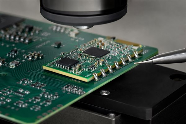
A module that was previously reflowed during its own assembly will experience another thermal cycle when mounted to the carrier. Component, laminate, and solder-joint exposure therefore belongs in the assembly review, especially for reworked or moisture-sensitive modules.
Which Solder Defects Occur at Castellated PCB Edges?
The main Castellated PCB edge-joint defects are opens, partial wetting, bridging, excess solder, module lift, and contamination, but the visible symptom does not identify the cause by itself. Diagnosis should connect the joint appearance to paste deposition, pad geometry, module condition, placement, and thermal history.
| Observed Defect | Likely Process Cause | Evidence to Check | Corrective Direction |
| Open or weak fillet | Low paste volume, poor wetting, edge contamination, module lift, or inadequate pad overlap | Stencil aperture, paste inspection, edge condition, coplanarity, and profile data | Restore wettable surfaces and validate deposit, support, and land pattern |
| Bridge between half-holes | Excess paste, tight mask spacing, placement offset, or solder drawn from a nearby through hole | Paste height, mask image, X-Y placement record, and neighboring pad geometry | Reduce or reshape the deposit and correct spacing or placement |
| Excess side solder | Oversized aperture, large exposed carrier pad, or uneven module seating | Stencil data, carrier footprint, module height, and joint-to-joint variation | Balance deposit volume and module support before changing reflow temperature |
| Lifted corner or rotated module | Unequal wetting forces, board warp, placement error, or inconsistent paste volume | Coplanarity, placement image, paste inspection, and corner-height measurement | Correct support, deposition balance, and placement references |
| Intermittent connection | Partial barrel damage, cracked fillet, contamination, or mechanical loading after assembly | Magnified edge inspection, continuity under controlled movement, and failure-location analysis | Separate fabrication damage from assembly and system-level mechanical stress |
Reworking one visible joint may hide a row-level process problem. Compare several joints across the module, including both ends of each row, before deciding whether the defect is isolated or caused by systematic alignment, paste, or routing variation.
How Should Castellated Holes and Solder Joints Be Inspected?
Castellated PCB inspection should cover the bare module edge before assembly and the completed fillets afterward, using acceptance criteria tied to the drawing, joint function, and agreed workmanship standard. A cosmetic photograph is not enough; the record should identify the view, magnification, sample plan, defect limits, and disposition.
- Bare-edge inspection: Check remaining barrel copper, routed-edge smoothness, burrs, plating folds, mask encroachment, exposed conductors, and laminate separation. Measure pitch and board dimensions when fit to the carrier is sensitive.
- Paste inspection: Verify deposit position, area, and repeatability on the carrier pads before placement. Compare the result with the approved stencil revision rather than relying on nominal CAD apertures.
- Post-reflow optical inspection: Confirm module alignment, visible wetting, bridge clearance, fillet continuity, corner seating, and residue condition from repeatable viewing angles.
- Hidden-joint assessment: Use X-ray or another suitable method only when the joint geometry or underside connections contain information that optical inspection cannot reveal. State what the image must prove before ordering the test.
- Traceable disposition: Link each defect image to the board lot, assembly lot, module position, defect code, reviewer, and rework or rejection decision. This record supports root-cause analysis if failures recur.
Supplier-specific notes can also reveal what a low-cost service treats as best-effort rather than a controlled capability. For example, OSH Park documents possible plating stubs and manual cleanup in its service context; a production order should instead state the delivered edge condition it requires.
How Do Panelization and Depanelization Affect Castellated Edges?
Castellated PCB panelization must support the module through fabrication and assembly without placing break tabs, router entry marks, or depanelization loads on functional plated half-holes. Panel rails and tab locations therefore need approval before production, not after the first edge is damaged.
- Support path: Place rails and tabs where they can carry drilling, plating, routing, finish, handling, and assembly loads without flexing the narrow module body.
- Functional-edge protection: Keep tabs and scoring away from plated half-holes unless the supplier has an explicitly approved process for the proposed geometry.
- Tool access: Provide router approach and exit space that does not force an unstable tool path across copper-dense edges or nearby components.
- Depanelization method: State whether boards are routed free, tab-routed, or separated after assembly, along with the allowed burr and edge-cleanup condition.
- Mechanical verification: Inspect samples from different panel positions because edge quality can vary with support, tool wear, and routing direction across the panel.
A fully castellated perimeter may leave no suitable location for panel tabs. That geometry should trigger an early panelization review because a late compromise can sacrifice functional edge length or introduce manual separation work that was not included in the quote.
Which Electrical and Mechanical Tests Should Be Specified?
Testing should prove the functions and loads assigned to the castellated connection, not merely confirm that the assembly powers on once. The acceptance plan needs the applied condition, measurement point, limit source, sample size, and output record for every required test.
- Continuity and isolation: Measure the required nets and adjacent-net isolation using limits from the released schematic, product requirement, or test specification. Record failures by module position and pin.
- Functional operation: Exercise interfaces, power rails, programming paths, and communications at the specified supply, load, and environmental condition. A simple boot indication does not cover intermittent edge joints.
- Mechanical retention: If the module experiences handling, shock, vibration, or connector forces, establish a product-relevant load path and acceptance condition. Do not invent a pull-force limit without a design requirement and validated fixture.
- Thermal cycling or aging: Use only when the product risk assessment requires it, with temperature range, dwell, transition, cycles, powered state, and post-test checks stated in the test plan.
- Failure analysis: Preserve the operating state and joint condition before rework. Localize electrical symptoms first, then correlate them with edge images, cross-sectioning, or material analysis when destructive evidence is justified.
Test coupons and sample modules should match the production stackup, finish, edge routing, carrier pad geometry, paste process, and reflow exposure. A simplified coupon can validate one mechanism, but it cannot replace assembly-level verification when the load path or thermal history is different.
What Changes Castellated PCB Cost and Lead Time?
Cost and schedule change when the edge geometry requires tighter routing control, special panel support, additional inspection, extra test coverage, or repeated engineering confirmation. The fastest way to stabilize a quote is to submit complete, internally consistent files and identify which criteria are mandatory.
| Cost Driver | Why It Changes Work | How to Reduce Uncertainty |
| Fine pitch or small remaining barrel | Consumes more drill-to-route registration margin and may require tighter inspection | Submit the exact outline, finished hole, pad geometry, and acceptable split condition |
| Castellations on several edges | Reduces space for panel tabs and complicates support during routing and assembly | Approve a panel drawing before the order is released |
| Special finish or storage control | Adds material, process, handling, packaging, or shelf-life requirements | Name the finish and packaging requirement in the purchase specification |
| Assembly and rework access | Changes stencil development, placement support, inspection, and repair labor | Provide module and carrier assembly data plus rework limits |
| Custom inspection or testing | Requires fixtures, programming, measurements, records, and additional review | State the method, sample plan, limits, and required report format |
A repeat Castellated PCB order can move more predictably when the approved panel, CAM decisions, stencil revision, profile, inspection criteria, and test records remain under revision control. Any change to hole geometry, outline, finish, carrier footprint, or module components should reopen the affected approval rather than being treated as a purchasing-only change.
What Files Should Be Included in a Castellated PCB RFQ?
An accurate RFQ needs fabrication data, module and carrier assembly data, acceptance criteria, quantity, and revision identity in one consistent package. The supplier should not have to infer the routed half-hole intent from a rendering or reconstruct the carrier footprint from a datasheet image.
- Fabrication package: Supply Gerber or ODB++, NC drill files, board outline, stackup, copper requirements, finish, solder-mask data, dimensions, tolerances, and a drawing that identifies every castellated edge.
- Panel requirements: State delivery format, permitted rails and tabs, tooling needs, fiducials, break-off method, and the edge condition required after separation.
- Assembly package: Provide the BOM, centroid data, module and carrier drawings, polarity marks, paste and stencil requirements, placement constraints, and reflow limitations.
- Inspection plan: Specify bare-edge views, solder-joint criteria, magnification, sample plan, defect disposition, required images, and any dimensional report.
- Test package: Include the test method, fixture interface, firmware or programming instructions, input conditions, measurement points, limits, sample quantity, and report format.
- Commercial inputs: Specify prototype and production quantities, delivery destination, target schedule, packaging, traceability, approved substitutions, and change-control contacts.
Before sending the RFQ, compare the file revision printed on the fabrication drawing, assembly drawing, BOM, centroid file, test instruction, and purchase request. A mixed-revision package can produce a technically valid quote for the wrong module.
What Castellated PCB Services Can EBest Circuit Provide?
EBest Circuit can review and quote PCB design support, prototype fabrication, mass production, component sourcing, and PCB assembly for projects that use castellated modules. The usable scope for a specific board is confirmed from its geometry, materials, quantity, carrier-board data, inspection needs, and test requirements.
- Design and DFM review: Submit the drill, outline, pad, stackup, panel, carrier-footprint, and assembly data so open manufacturability questions can be consolidated before release.
- Prototype fabrication: Use the first build to verify routed-edge condition, module dimensions, carrier fit, solder deposition, and inspection criteria before production quantities are committed.
- Production fabrication: Freeze the approved CAM decisions, panel arrangement, finish, edge criteria, and change-control baseline for repeat orders.
- Component sourcing and assembly: Provide the BOM, approved manufacturer list, module handling limits, stencil data, placement information, reflow requirements, and rework boundaries.
- Inspection and testing: Specify the required edge images, solder-joint checks, electrical tests, fixtures, programming method, sample plan, and report format in the quotation package.
Order-specific capability, schedule, certificates, inspection records, and test coverage should be confirmed in the written quotation and engineering response. This ties the sourcing decision to the released board and its documented acceptance requirements.
FAQs About Castellated PCB Manufacturing and Assembly
Q1: Are castellated holes the same as ordinary plated through holes?
A1: No. A castellated feature begins as a plated hole, but the finished board outline removes part of the barrel. That extra routing operation changes copper support, edge quality, inspection access, and how the feature is soldered to another board.
Q2: Must exactly half of every plated hole remain?
A2: The required remaining geometry must be agreed with the selected fabricator. A nominal half-hole is common, but the drawing should state the intent and the supplier should confirm what drill-to-route registration and inspection limits it can control.
Q3: Can castellated edges use any surface finish?
A3: Finish selection is process-specific. The edge geometry, hole size, storage period, soldering method, and supplier capability all matter. Name the finish in the RFQ and obtain written confirmation for the proposed construction.
Q4: Can components be placed on both sides of a castellated module?
A4: Only when the carrier design provides the required underside clearance and assembly method. A flat-mounted module usually needs a component-free underside contact area, while a raised or recessed arrangement requires explicit mechanical and solder-joint design.
Q5: Can a castellated module be hand soldered?
A5: Hand soldering is practical for prototypes and rework when the joints remain accessible. The work instruction should control alignment, flux, heat exposure, solder amount, cleanliness, and inspection so manual results can be evaluated consistently.
Q6: Why does solder sometimes disappear into a nearby hole?
A6: An open through hole can wick molten solder away from the intended edge joint. Review the connected pad geometry, mask separation, paste deposit, and hole treatment instead of compensating with uncontrolled extra solder.
Q7: Does a certified radio module make the completed product certified?
A7: Module certification does not automatically approve the finished product. The host board, antenna implementation, enclosure, power conditions, labeling, and destination requirements may still need product-level review or testing.
Q8: Should every castellated solder joint be X-rayed?
A8: Use X-ray only when it reveals required information that optical inspection cannot show. Visible side fillets may be evaluated optically, while hidden underside connections or internal anomalies need a method selected for the actual failure risk.
Q9: Can a damaged plated half-hole be repaired with solder?
A9: Solder cannot restore missing barrel adhesion or laminate strength. Cosmetic wetting may hide torn copper or delamination, so the defect must be classified before a documented rework method is accepted.
Q10: What should be checked on the first assembled sample?
A10: Check module fit, alignment, joint wetting, bridge clearance, corner seating, electrical function, and the evidence required for production release. Retain the approved module, carrier, stencil, profile, inspection images, test record, and deviations as the baseline.
Conclusion
A successful castellated module starts with one controlled chain from plated-hole geometry to carrier footprint, solder process, inspection, and test evidence. Specify the routed edge and panel support before fabrication, validate paste and placement on representative assemblies, and release production only after the visible edge condition and functional checks meet the agreed acceptance plan.
For an engineering review and quotation, send your Gerber or ODB++, NC drill, stackup, BOM, module and carrier drawings, quantity, panel requirements, inspection plan, and test instructions to sales@bestpcbs.com. The quotation can then identify confirmed scope, remaining engineering questions, and the records required for prototype or production approval.
You may also like





Tags: Castellated Holes, Castellated PCB, PCB Assembly, PCB inspection