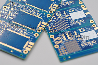
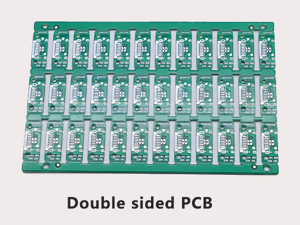
PCB coatings are protective layers applied to printed circuit board assemblies to improve reliability in demanding environments. They help protect electronic components, solder joints, and conductive traces from moisture, corrosion, dust, chemicals, salt spray, vibration, and temperature changes.
Choosing the right PCB coating type is important for product lifespan, electrical safety, field reliability, and long-term cost control. This guide explains the main coating materials, how they work, where they are used, how they compare, and what buyers should check before placing an order.
What Are PCB Coating Types?
PCB coating types refer to different protective materials used to cover printed circuit boards after assembly. These coatings form a thin insulating barrier over exposed conductive areas while allowing the circuit to function normally.
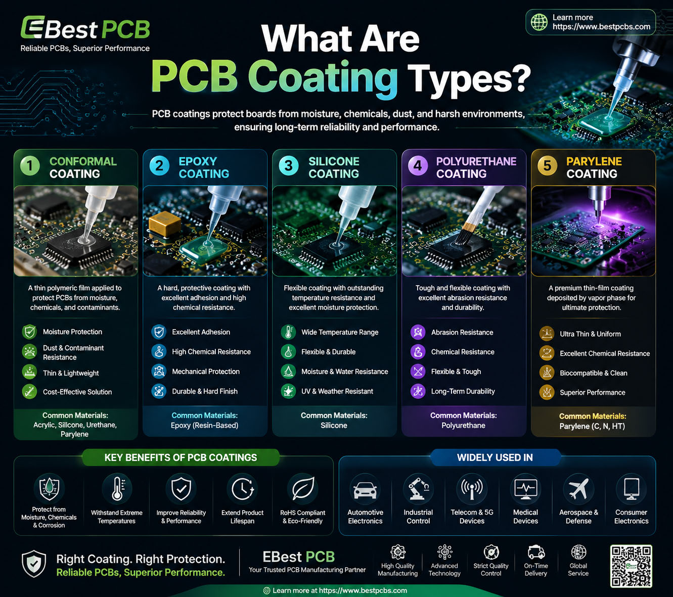
The most common PCB coating types include acrylic coating, silicone coating, polyurethane coating, epoxy coating, Parylene coating, and nano coating. Each coating has different strengths in moisture resistance, chemical resistance, temperature resistance, flexibility, repairability, and cost.
Why Are PCB Coatings Important?
Electronic assemblies can fail when moisture, dust, chemical residues, salt ions, or conductive contamination reach the PCB surface. These conditions may cause corrosion, leakage current, insulation degradation, dendrite growth, and short circuits.
PCB coatings help improve reliability by reducing environmental damage and protecting sensitive circuits during long-term operation.
- Protect copper traces and solder joints from corrosion
- Improve insulation resistance
- Reduce leakage current
- Prevent moisture-related failures
- Improve reliability in harsh environments
- Extend product service life
- Reduce maintenance and warranty costs
How Do PCB Coatings Work?
PCB coatings work by creating a physical and electrical barrier between the circuit board and the external environment. This barrier blocks or reduces the contact between conductive surfaces and moisture, oxygen, chemicals, dust, and salt contamination.
| Protection Function | Purpose |
|---|---|
| Moisture Protection | Prevents water vapor from reaching conductive surfaces |
| Corrosion Protection | Isolates metal surfaces from oxygen and contaminants |
| Electrical Insulation | Reduces leakage current and improves dielectric performance |
| Chemical Resistance | Protects against solvents, oils, fuels, and industrial chemicals |
| Mechanical Protection | Reduces damage caused by vibration, shock, and handling |
| Thermal Stability | Maintains coating performance during temperature cycling |
What Types of PCB Coatings Are Available?
Acrylic Coatings
Acrylic coatings are widely used because they are cost-effective, easy to apply, and easy to repair. They provide good moisture protection for general electronic products and are suitable for many commercial and industrial applications.
Advantages:
- Low cost
- Fast drying
- Easy inspection
- Excellent reworkability
- Good moisture resistance
Limitations:
- Moderate chemical resistance
- Limited high-temperature performance
- Lower durability than polyurethane or Parylene coating
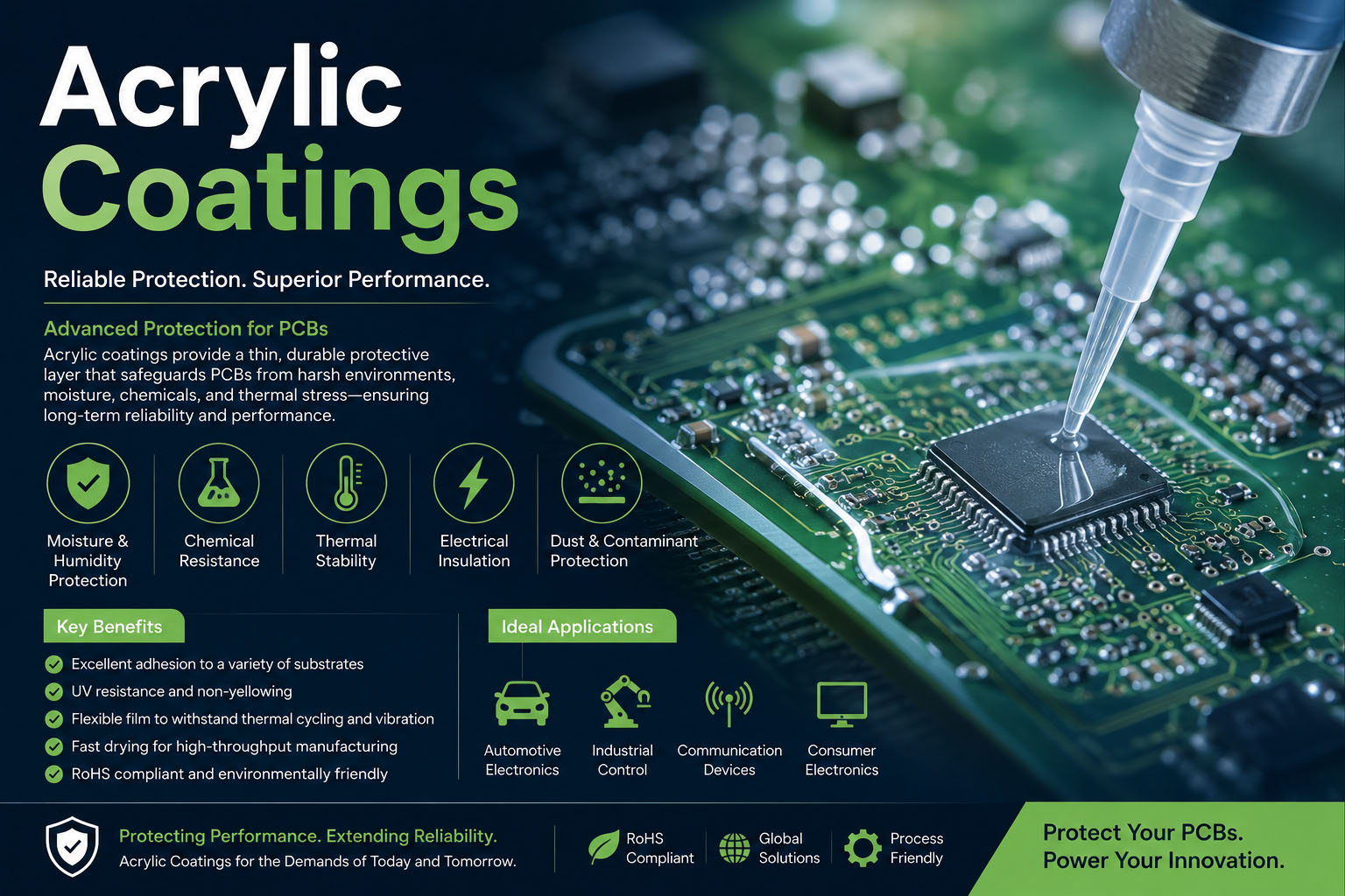
Common applications: consumer electronics, communication equipment, control boards, and indoor industrial electronics.
Silicone Coatings
Silicone coatings offer excellent flexibility and strong performance under high temperature, low temperature, humidity, and vibration. They are commonly used in outdoor electronics and automotive applications.
Advantages:
- Excellent thermal stability
- Good flexibility
- Strong humidity resistance
- Good vibration resistance
- Suitable for thermal cycling environments
Limitations:
- Higher cost than acrylic coating
- More difficult to remove for repair
Common applications: automotive electronics, LED lighting, outdoor equipment, renewable energy systems, and power modules.
Polyurethane Coatings
Polyurethane coatings provide strong resistance to moisture, solvents, chemicals, abrasion, and salt spray. They are suitable for harsh industrial and marine environments where corrosion risk is high.
Advantages:
- Excellent chemical resistance
- Strong moisture barrier
- Good abrasion resistance
- Good salt spray protection
Limitations:
- Difficult rework
- Longer curing time
Common applications: industrial automation, marine electronics, oil and gas equipment, and chemical processing systems.
Epoxy Coatings
Epoxy coatings create a hard and durable protective layer with strong adhesion and high mechanical strength. They are often used when the PCB requires strong physical protection and chemical resistance.
Advantages:
- High mechanical strength
- Strong adhesion
- Excellent chemical resistance
- Durable protection
Limitations:
- Limited flexibility
- Difficult to remove or repair
- May not be suitable for components exposed to high mechanical stress from thermal expansion
Common applications: power electronics, industrial control systems, heavy-duty equipment, and high-reliability modules.
Parylene Coatings
Parylene coating is applied through a chemical vapor deposition process under vacuum conditions. It forms a highly uniform, thin, and pinhole-free protective layer, even around complex geometries and small component gaps.
Advantages:
- Uniform coverage
- Pinhole-free protection
- Extremely low moisture vapor transmission rate
- Excellent dielectric properties
- Outstanding corrosion protection
Limitations:
- Higher processing cost
- Specialized equipment required
- Difficult rework
Common applications: medical devices, aerospace electronics, defense systems, sensors, and high-reliability electronic assemblies.
Nano Coatings
Nano coatings create an ultra-thin hydrophobic layer on the PCB surface. They are mainly used for lightweight moisture protection in compact electronics where coating thickness must be minimized.
Advantages:
- Very thin coating layer
- Lightweight protection
- Minimal effect on component dimensions
- Good water-repellent performance
Limitations:
- Lower protection than Parylene coating
- Limited performance in extreme industrial environments
Common applications: smartphones, wearable devices, portable electronics, and consumer electronic products.
What Materials Are Used in PCB Coatings?
The coating material determines the protection level, repairability, curing process, and long-term reliability of the PCB assembly.
| Material | Key Characteristic | Typical Use |
|---|---|---|
| Acrylic Resin | Cost-effective and easy to repair | General electronics |
| Silicone Polymer | Flexible and thermally stable | Automotive and outdoor electronics |
| Polyurethane Resin | Strong chemical resistance | Industrial and marine electronics |
| Epoxy Resin | High mechanical strength | Power and heavy-duty electronics |
| Poly-Para-Xylylene | Uniform vapor-deposited protection | Medical, aerospace, and defense electronics |
| Nano Polymers | Ultra-thin hydrophobic protection | Compact consumer electronics |
What Are the Advantages of PCB Coatings?
PCB coatings provide multiple reliability benefits for electronic products used in demanding environments.
- Improved moisture resistance
- Better corrosion protection
- Enhanced electrical insulation
- Reduced risk of short circuits
- Improved protection against dust and contamination
- Longer service life
- Higher field reliability
For many industrial, automotive, medical, and outdoor applications, coating is an important process for reducing failure risk and improving product stability.
What Are the Limitations of PCB Coatings?
PCB coatings improve protection, but they also introduce additional manufacturing and design considerations.
- Additional material and processing cost
- Longer production cycle
- Possible repair difficulty
- Masking requirements for connectors and test points
- Inspection complexity
- Compatibility concerns with certain components or materials
The best coating choice should balance protection level, application environment, cost, production volume, and maintenance requirements.
How Do Different PCB Coatings Compare?
| Coating Type | Moisture Protection | Chemical Resistance | Temperature Resistance | Reworkability |
|---|---|---|---|---|
| Acrylic | Good | Moderate | Moderate | Excellent |
| Silicone | Excellent | Good | Excellent | Moderate |
| Polyurethane | Excellent | Excellent | Good | Difficult |
| Epoxy | Excellent | Excellent | Very Good | Very Difficult |
| Parylene | Outstanding | Outstanding | Excellent | Difficult |
| Nano | Moderate | Moderate | Good | Good |
How Do You Choose the Right PCB Coating?
The right PCB protective coating depends on the actual operating environment and product reliability target. A coating that works well for consumer electronics may not be suitable for automotive, marine, aerospace, or medical applications.
Key selection factors include:
- Operating temperature range
- Humidity exposure
- Salt spray exposure
- Chemical exposure
- UV exposure
- Vibration and mechanical stress
- Repair and rework requirements
- Required coating thickness
- Compliance standards
- Total project budget
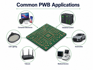
Which Industries Use PCB Coatings?
PCB coatings are widely used in industries where electronic reliability is critical.
Automotive Electronics
Automotive PCB assemblies must withstand temperature cycling, vibration, humidity, and road salt. Common applications include engine control units, battery management systems, ADAS modules, lighting control systems, and power distribution modules.
Industrial Automation
Industrial control boards are often exposed to dust, oil mist, vibration, humidity, and electrical noise. PCB coatings help protect PLC controllers, sensors, motor drives, robotics systems, and power control modules.
Medical Devices
Medical electronics require high reliability, stable insulation, and clean protection. Parylene coating is often used in medical devices because it provides uniform barrier protection and strong dielectric performance.
Aerospace and Defense
Aerospace and defense electronics require long-term reliability under harsh operating conditions. Coatings are used in flight control systems, radar equipment, satellite electronics, navigation systems, and communication modules.
Renewable Energy
Solar inverters, wind turbine controllers, and energy storage systems often operate in outdoor or semi-outdoor environments. PCB coatings help reduce moisture damage and corrosion risk.
What Design Considerations Are Important Before Applying PCB Coating?
PCB coating should be considered during the design stage, not only after assembly. Proper design planning can reduce coating defects and make production easier.
- Define areas that require masking
- Keep connectors and test points accessible
- Check component spacing and coating flow
- Review thermal dissipation requirements
- Confirm material compatibility
- Consider future repair needs
- Avoid trapping residues under the coating
What Manufacturing Methods Are Used for PCB Coating?
Spray Coating
Spray coating is suitable for medium- and high-volume production. It provides efficient coverage and can be automated for better consistency.
Dip Coating
Dip coating provides broad coverage by immersing the PCB assembly into coating material. It is effective for simple board designs but may produce thicker coating layers.
Selective Coating
Selective coating uses automated equipment to apply coating only to required areas. It improves precision, reduces masking work, and helps control material usage.
Brush Coating
Brush coating is commonly used for prototypes, repairs, and small production runs. It is flexible but less consistent than automated coating methods.
Chemical Vapor Deposition
Chemical vapor deposition is used for Parylene coating. It provides highly uniform protection and can cover complex shapes, edges, and small gaps.
What Industry Standards Apply to PCB Coatings?
Industry standards help define coating material performance, inspection requirements, and assembly quality expectations.
IPC-CC-830
IPC-CC-830 defines qualification and performance requirements for conformal coating materials used on electronic assemblies.
IPC-A-610
IPC-A-610 provides acceptance criteria for electronic assemblies, including workmanship and inspection requirements.
UL Certification
UL certification helps evaluate material safety, flammability, and electrical performance for specific applications.
RoHS Compliance
RoHS compliance restricts hazardous substances in electronic products and is important for products sold into many global markets.
REACH Compliance
REACH regulates chemical substances used in manufacturing and supports safer material selection for international supply chains.
How Are PCB Coatings Tested?
Testing helps verify whether the coating has been applied correctly and whether it can meet the expected reliability requirements.
- Visual inspection
- UV fluorescence inspection
- Coating thickness measurement
- Adhesion testing
- Salt spray testing
- Thermal cycling testing
- Humidity testing
- Insulation resistance testing
What Are the Most Common PCB Coating Failures?
Common PCB coating failures are usually related to poor cleaning, incorrect coating thickness, improper curing, or weak process control.
- Delamination
- Cracking
- Blistering
- Pinholes
- Poor adhesion
- Incomplete coverage
- Contamination trapped under the coating
Many coating failures can be prevented through proper cleaning, controlled application parameters, validated curing conditions, and regular inspection.
How Can PCB Coating Defects Be Prevented?
Defect prevention starts before the coating process. The PCB assembly should be clean, dry, and compatible with the selected coating material.
- Use proper cleaning before coating
- Control humidity and temperature during application
- Validate coating thickness
- Use correct curing conditions
- Mask connectors and contact areas carefully
- Inspect boards under UV light when applicable
- Record process parameters for traceability
What Factors Affect PCB Coating Costs?
PCB coating cost depends on the coating material, process method, board complexity, production quantity, masking requirements, and testing specifications.
- Coating material type
- PCB size and layout complexity
- Coating thickness
- Production volume
- Application method
- Masking difficulty
- Inspection and testing requirements
- Certification requirements
Acrylic coating is usually more economical, while Parylene coating generally has higher processing costs because it requires specialized vacuum deposition equipment.
How Can Buyers Ensure PCB Coating Quality?
Buyers should not evaluate coating quality only by price. A reliable PCB coating supplier should provide stable process control, material traceability, inspection capability, and engineering support.
- Confirm coating material specifications
- Check IPC and compliance requirements
- Review inspection methods
- Ask for coating thickness control capability
- Confirm masking and process requirements
- Check production traceability
- Evaluate supplier experience with similar applications
How Do You Choose a Reliable PCB Coating Supplier?
A reliable PCB coating supplier should understand both the coating process and the final application environment. This is especially important for automotive, industrial, medical, aerospace, and outdoor electronic products.
- Experience with different PCB coating types
- Engineering support for material selection
- Stable coating and curing process
- Inspection and testing capability
- Quality documentation and traceability
- Prototype and mass production support
- Global delivery experience
What Should Be Checked Before Placing a PCB Coating Order?
Before placing an order, buyers should clearly define the technical and quality requirements. This helps reduce misunderstanding and prevents delays during production.
- Application environment
- Coating material type
- Required coating thickness
- Masking areas
- Testing standards
- Documentation requirements
- Lead time
- Packaging requirements
Frequently Asked Questions About PCB Coating Types
What is the most commonly used PCB coating?
Acrylic coating is one of the most commonly used PCB coatings because it is cost-effective, easy to apply, and easy to rework. It is suitable for many commercial and general industrial electronics.
Which PCB coating provides the best moisture protection?
Parylene coating usually provides the strongest moisture protection because it forms a uniform, pinhole-free barrier with very low moisture vapor transmission. Silicone and polyurethane coatings also perform well in humid environments.
Is Parylene better than silicone coating?
Parylene provides better barrier protection and uniform coverage, while silicone offers better flexibility and thermal cycling performance. The better choice depends on the operating environment and reliability requirement.
Which coating is recommended for outdoor electronics?
Silicone coating is often recommended for outdoor electronics because it performs well under temperature changes, humidity, UV exposure, and vibration. For more demanding environments, polyurethane or Parylene may be considered.
Can PCB coatings extend product lifespan?
Yes. PCB coatings can extend product lifespan by reducing moisture damage, corrosion, contamination, leakage current, and electrical failure risk. Proper coating selection can improve long-term reliability.
How thick should a PCB coating be?
Most conformal coatings are applied within a controlled thickness range based on material type and application requirements. The correct thickness should meet the required protection level without affecting connectors, heat dissipation, or repairability.
Are PCB coatings repairable?
Some PCB coatings are easier to repair than others. Acrylic coating is generally the easiest to remove and rework, while epoxy and Parylene coatings are more difficult to repair.
Which coating is best for automotive electronics?
Silicone coating is frequently used in automotive electronics because it provides strong temperature resistance, flexibility, and vibration protection. Polyurethane may also be used when chemical or salt spray exposure is important.
What standards should PCB coatings comply with?
Common standards and compliance requirements include IPC-CC-830, IPC-A-610, UL certification, RoHS, and REACH. The exact requirement depends on the product application and target market.
What causes PCB coating failure?
PCB coating failure is often caused by poor cleaning, trapped contamination, incorrect curing, excessive thickness, poor adhesion, or unsuitable coating selection. Stable process control is essential for preventing failures.
Conclusion
PCB coating types play an important role in improving the reliability, durability, and service life of electronic assemblies. Acrylic, silicone, polyurethane, epoxy, Parylene, and nano coatings each provide different levels of moisture protection, chemical resistance, temperature resistance, flexibility, and repairability.
For general electronics, acrylic coating offers a practical balance of cost and protection. For automotive and outdoor applications, silicone coating is often preferred because of its flexibility and thermal stability. For industrial, marine, medical, aerospace, and high-reliability applications, polyurethane, epoxy, or Parylene coating may provide stronger protection.
When selecting a PCB coating, engineers and buyers should evaluate the application environment, coating material, quality standards, inspection requirements, repair needs, and total lifecycle cost. A reliable supplier can help choose the most suitable PCB protective coating and provide stable production quality from prototype to mass production.
If you are looking for reliable OEM manufacturing, ODM production, prototype development, mass production, or custom engineering solutions, please contact our engineering team for technical support and quotation services.