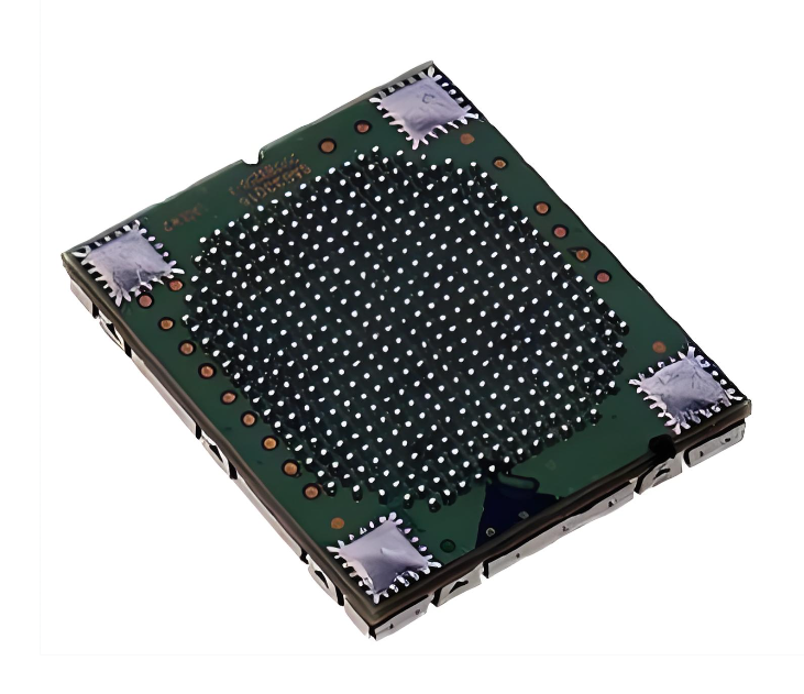
WLCSP assembly connects a chip-sized device to PCB pads through a fine-pitch array of solder balls. Those small connections save board space, but leave little room for uneven paste deposits, misplaced solder mask or rough handling. Reliable assembly depends on matching the footprint and process to the actual component—not simply selecting a recipe marked “0.4 mm pitch.”
EBest Circuit combines PCB fabrication, component sourcing and PCB assembly, allowing board construction and assembly requirements to be reviewed together. For a project containing WLCSP devices, contact sales@bestpcbs.com to discuss the component package and proposed PCB layout before the build.
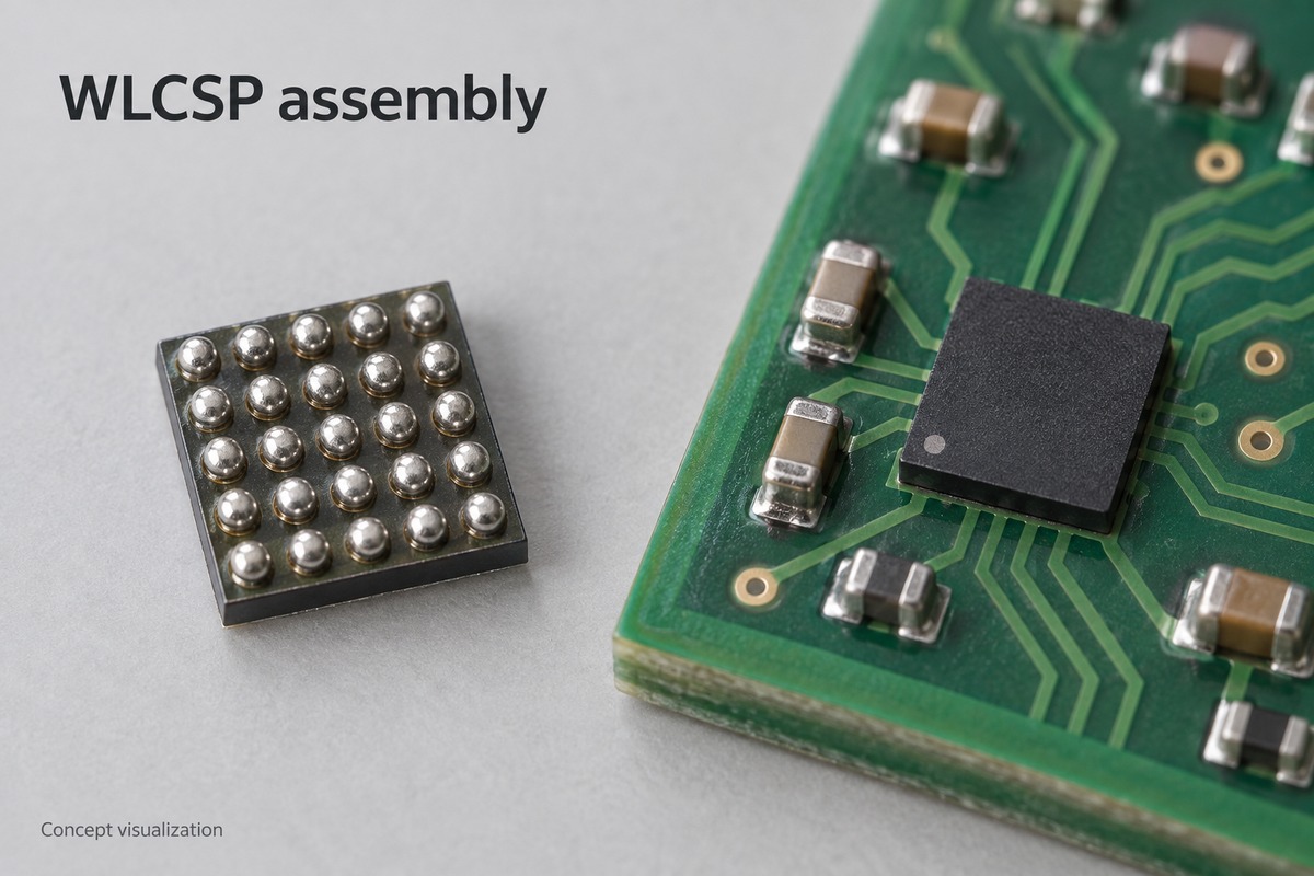
What Is WLCSP Assembly on a PCB?
Board-level WLCSP assembly mounts an already packaged semiconductor device onto a circuit board. It is separate from the wafer-level processing that creates the package.
WLCSP stands for wafer-level chip-scale package. In a conventional fan-in WLCSP, the connections sit beneath the silicon die, within its footprint. There is no larger leadframe or laminate package substrate extending around it.
The board assembly still uses solder-paste printing, component placement and reflow. The difference is the small soldering geometry and exposed, mechanically sensitive package. Ball pitch describes spacing; it does not specify ball diameter, pad shape or handling limits.
How Do PCB Pads and Vias Affect WLCSP Solder Joints?
The exposed pad area controls where solder can wet, while the via structure can disturb the solder volume beneath a ball.
| Pad construction | Exposed soldering surface |
|---|---|
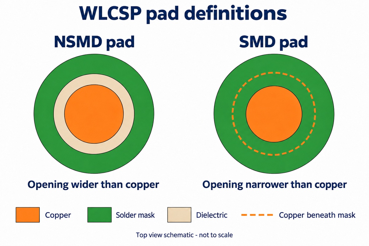
| Non-solder-mask-defined (NSMD) | The mask opening is larger than the copper pad. Solder can wet the pad’s top and exposed edges. |
| Solder-mask-defined (SMD) | The mask opening is smaller than the copper pad. The opening defines the available soldering area. |
Here, SMD describes the pad definition, not a surface-mount device. Neither construction makes a footprint interchangeable between different WLCSP parts. The component’s land-pattern recommendation determines the appropriate geometry.
An unfilled via in a solder pad can trap air and contribute to voids or inconsistent joints. Where routing requires via-in-pad, a filled-via construction addresses this concern; the final pad surface still needs to meet the footprint requirements.
Mask registration also matters. A shifted opening can partly cover a pad that was correctly drawn in the CAD data.
How Does Stencil Design Control Solder Volume for WLCSP?
Stencil thickness and aperture geometry determine the paste available, but paste release determines how much actually reaches each pad.
A small aperture has relatively little opening area compared with its walls. Paste can remain inside instead of transferring cleanly to the PCB. Increasing stencil thickness adds potential volume while making release through that same small opening more difficult.
- Aperture geometry governs the deposit footprint and release behavior.
- Wall finish affects how readily paste separates from the stencil.
- Paste particle size must suit the small opening and printing process.
A mixed-component board may need more paste at larger parts than at the WLCSP. A locally thinner stencil region can accommodate that difference, provided its transition works with nearby apertures. Post-print inspection reveals missing, uneven or displaced deposits before the package covers them.
How Are WLCSP Devices Placed and Reflowed?
Placement must align the ball array without damaging the die; reflow must then form joints within the component and paste process limits.
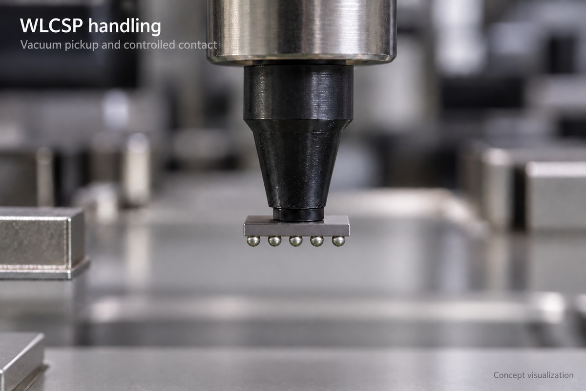
Vision alignment locates the device or its ball pattern. The pickup nozzle, placement height and applied force need to suit the package. A setup that handles a robust molded component successfully can still damage a small WLCSP.
Solder surface tension can help center the device during reflow, but that effect is not permission to accept arbitrary placement errors.
The thermal profile describes temperature at the assembly over time—not just the oven settings. Board loading, component location and neighboring parts affect heating. Profile measurements therefore need to represent the actual populated board.
A 260°C package qualification rating is not a universal reflow target. Peak temperature, time above liquidus and heating and cooling rates must satisfy the applicable component limits and solder-paste requirements together.
How Are Hidden WLCSP Solder Joints Inspected?
The hidden array needs inspection beyond a top-down view of the component. Different methods answer different questions.
| Method | What it can reveal | What it does not establish alone |
|---|---|---|
| Optical inspection | Visible damage, orientation and accessible joint edges | The condition of every joint beneath the die |
| X-ray inspection | Bridging, voiding and irregular solder distribution, subject to image quality and viewing angle | Electrical operation or lifetime under mechanical and thermal stress |
| Electrical testing | Opens, shorts or functional faults within the test coverage | The physical condition of every solder interface |
A suspicious connection may need further analysis. Cross-sectioning can expose an internal interface, but destroys the examined area and is better suited to process investigation than routine inspection of saleable boards.
A board that powers on has passed that particular test; it has not automatically demonstrated solder-joint durability.
When Does WLCSP Assembly Need Underfill?
Underfill is not automatically required for WLCSP. Renesas recommends assembly without it for the packages covered by its implementation guide, which were qualified without underfill.
Underfill occupies the gap around the joints and changes how mechanical and thermal loads reach them. An application with demanding drop or bending conditions may justify evaluating reinforcement, but adding resin is not automatically a reliability improvement.
The material’s thermal expansion, stiffness, cure conditions and compatibility with residues all matter. Filling behavior and the fillet around the die also affect the result. A suitable material and process need validation on the intended assembly.
Underfill additionally changes repair options. A process chosen for reinforcement may make later component removal much harder.
Can WLCSP Components Be Reworked?
Replacement can be possible, but it needs a controlled process and an intact PCB footprint. Renesas discourages routine rework; Microchip describes a replacement process and advises against reusing removed devices in final assemblies.
- Remove the device with controlled heating. Local heating and board preheating help release the soldered component without forcing it from the pads.
- Restore the mounting site. Residual solder must be removed without lifting copper or damaging the solder mask.
- Deposit paste and fit a new device. A miniature stencil and vision-assisted placement help reproduce the required soldering geometry.
- Reflow and verify the replacement. The repaired location needs inspection and appropriate electrical testing.
A successful removal does not prove the board is ready for reuse. Damaged pads, underfill and the assembly’s previous heat exposure can limit repair.
For a WLCSP assembly project, EBest Circuit can review the PCB and PCBA requirements against your selected component. Email sales@bestpcbs.com with the part number and available board files to discuss the proposed build.