PCB manufacturing PCB manufacturing
Home > Blog

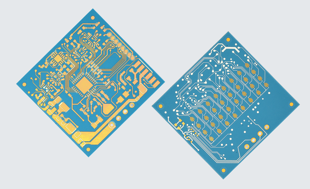
dpc ceramic pcb

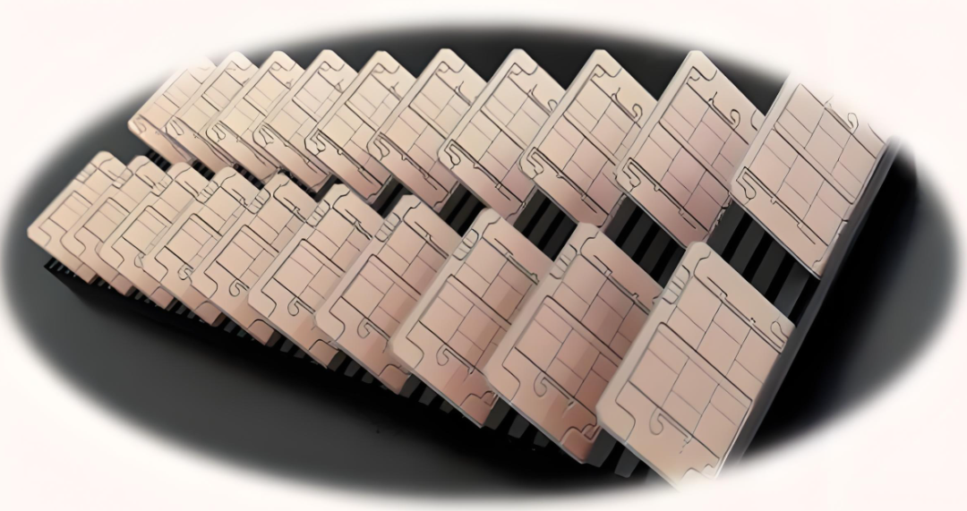
Manufacturing Si3N4 Ceramic Substrates for Power Modules
Thursday, September 3rd, 2026

At EBest Circuit (Best Technology), we manufacture Si3N4 ceramic circuit substrates for power electronics using AMB and DPC processes. As a Si3N4 substrate manufacturer, we build the patterned copper structure that connects power devices, transfers heat and maintains electrical isolation. For a power module, the manufacturing challenge is to make that structure work through repeated heating and cooling, not simply to choose a ceramic with a high conductivity number.
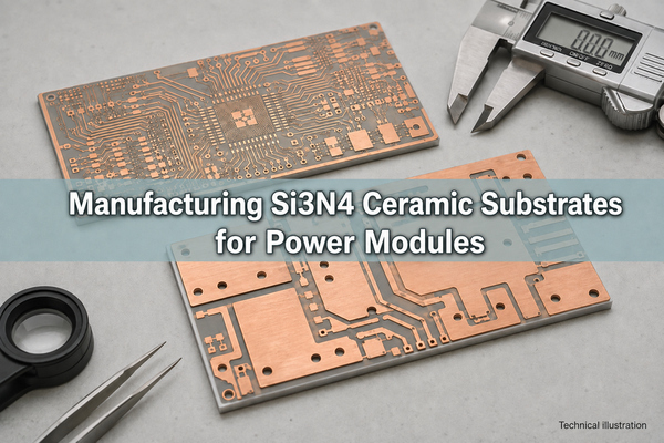
Manufacturing Si3N4 ceramic substrates for power modules, technical illustration

The Si3N4 chemical name is silicon nitride. In a silicon nitride ceramic substrate, the ceramic provides insulation while the metal layers form the circuit. Silicon carbide, or SiC, is different: a SiC semiconductor die can be mounted above a silicon nitride substrate, with each material performing a different job.

Why Do Thermally Cycled Power Modules Use Si3N4?

Power devices heat up under load and cool when the load falls. Copper and ceramic expand by different amounts, loading their bonded interface during each cycle. Si3N4 ceramic is attractive here because its resistance to crack propagation can support demanding copper-ceramic designs while retaining electrical insulation and a useful heat path.

This is why we consider the mechanical properties of silicon nitride alongside thermal performance. High silicon nitride thermal conductivity alone does not describe how a metallized substrate responds to copper thickness, edge defects or repeated temperature swings. The following Si3N4 material properties illustrate the different inputs to that decision.

Design input Electronic-substrate grade example Question it helps answer
Si3N4 thermal conductivity 85 W/m·K at 25°C How much thermal resistance does the ceramic thickness add?
Fracture toughness and bending strength 6.5 MPa·√m, indentation-fracture method; 800 MPa, three-point bending How does the selected grade resist crack growth and bending?
Si3N4 thermal expansion coefficient 2.6 ppm/K over 40–400°C What expansion mismatch must the copper-ceramic structure accommodate?
Si3N4 Young’s modulus 310 GPa How stiff is the ceramic in the mechanical model?

These are reference values for one commercial grade, not our finished-board acceptance limits. Use the selected grade’s silicon nitride coefficient of thermal expansion over the relevant temperature interval; a room-temperature value cannot describe an entire operating cycle.

Si3N4 properties make the material a strong candidate when mechanical reliability and heat removal must be addressed together. An AlN substrate may still be preferable where reducing ceramic-layer thermal resistance dominates the design, while alumina can suit less demanding, cost-sensitive circuits. The choice should follow the module’s loading and cooling requirements rather than a universal material ranking.

Building the Copper-Ceramic Structure with AMB

For a thick-copper power circuit, our AMB ceramic PCBs provide a manufacturing route that joins copper to the ceramic through active metal brazing. A Si3N4 AMB substrate combines current-carrying copper regions with an insulating ceramic core; the brazed interface connects the materials mechanically and thermally.

  1. Define the stack. We review the silicon nitride Si3N4 plate, copper on each face, finished dimensions and assembly surfaces against the circuit drawing.
  2. Join copper to ceramic. An active brazing material enables the metal-ceramic bond. This is a metallurgical joining layer, not an adhesive film.
  3. Form the isolated circuit regions. Patterning must define both the copper geometry and the required electrically isolated spaces. Conductive residues between islands cannot remain as unintended current paths.
  4. Finish the connection surfaces. We match the specified finish and pad condition to the subsequent attachment process before the circuit enters module assembly.

The copper thickness and isolation geometry must be developed together. Etching a thick conductor produces a sidewall profile, so the gap visible at the copper surface is not necessarily the same as the metal-free distance at the ceramic interface. We review the finished geometry, not only the artwork line.
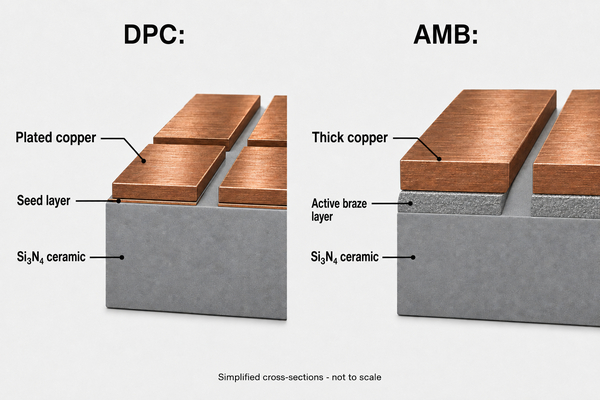
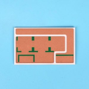
Simplified DPC and AMB Si3N4 ceramic circuit cross-sections with isolated copper patterns

Choosing DPC for Finer Si3N4 Circuit Geometry

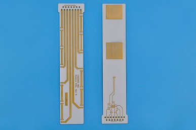
Not every silicon nitride circuit needs thick brazed copper. If the design requires finer conductor geometry or thinner controlled metallization, our DPC ceramic PCBs offer another route. Direct plated copper uses deposited metallization and copper plating to create patterned tracks and pads on the ceramic.

A smaller feature capability is useful when connection density drives the layout, but it does not make DPC an automatic substitute for an AMB substrate carrying a different current or heat load. We select the route against the conductor structure and attachment requirements before applying the dimensional limits below.

Our Si3N4 Substrate Manufacturing and Customization Capabilities

We manufacture custom Si3N4 ceramic circuits with the copper layout, board outline and connection surfaces specified for the project. The following DPC and AMB process capabilities establish a starting point for engineering review; they are not a promise that every maximum and minimum can be combined on the same board.

Item Our DPC process Our AMB process
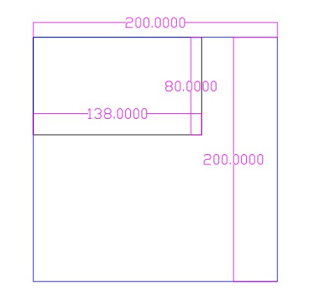
Maximum panel size 138 × 190 mm 114 × 114 mm
Copper thickness 2–200 ”m 8–22.9 oz, about 0.28–0.80 mm
Minimum line / space 6 / 8 mil, about 0.15 / 0.20 mm 20 / 20 mil, about 0.50 / 0.50 mm
Circuit layers Two-layer capability Two-layer capability
Surface finish options OSP, ENIG, immersion silver OSP, ENIG, immersion silver

Customization covers the conductor pattern, pad locations, outline, hole positions and specified finish. We confirm ceramic grade and thickness with the copper construction rather than applying a generic ceramic thickness list to every Si3N4 build. Panel dimensions also include manufacturing margins; they are not the usable circuit area.

Design Details We Review Before Circuit Fabrication

A manufacturable substrate drawing describes more than an outline and a copper thickness. Our custom ceramic PCB manufacturing review connects the circuit artwork to the joining process, mechanical support and electrical isolation requirements.

Drawing or assembly input Our manufacturing review Why it matters
Copper islands, line spacing and thickness Review patterning allowance, pad shape and the required isolation after metal removal Heavy copper changes achievable geometry; narrow gaps require more than a nominal artwork dimension
Ceramic outline, holes and registration references Check the mechanical drawing against the copper artwork and assembly datums The circuit must align with the device placement, terminals and module mounting arrangement
Working voltage, ceramic thickness and conductor separation Define insulation test conditions and review clearance and creepage with the module design A material breakdown number is not the assembled module’s working-voltage rating

Material Data Needed Beyond the Copper Drawing

For electrical modeling, Si3N4 permittivity is grade- and frequency-dependent; an electronic-substrate example is 7.8 at 1 MHz. The electrical conductivity of silicon nitride is low in its insulating substrate form, so current should follow the copper rather than pass through the ceramic. Parasitic capacitance across that ceramic still matters in a fast-switching module.

Si3N4 density and Si3N4 hardness serve different manufacturing purposes: a grade example lists 3.22 g/cmÂł and 15 GPa Vickers hardness. Density contributes to mass estimates; hardness informs machining considerations. Neither replaces fracture-toughness or edge-quality requirements when assessing a thin circuit plate.

Controlling Warpage and Edge Stress in Thick-Copper Si3N4 Substrates

Warpage control starts with the copper-ceramic construction, not just a flatness check at shipment. Copper on the two faces can differ in thickness, coverage and pattern position. Those differences, together with ceramic thickness and substrate dimensions, affect how the part bends as the bonded structure changes temperature.

During layout review, we examine the relationship between the front and back copper patterns, large copper islands, ceramic borders and assembly support points. Symmetry can help, but forcing identical copper on both faces may conflict with the electrical design. An asymmetric stack needs its own assessment rather than a universal rule that one copper ratio guarantees flatness.

At the perimeter, copper geometry, the metal-free ceramic border and existing edge defects influence local loading. Thick copper should not simply be extended to the ceramic edge to gain conductor area. We agree the relevant clearances and edge-acceptance criteria for the selected stack.

For a demanding mounting interface, the drawing should define the flatness measurement area and support condition. Initial samples can then be checked against the intended attachment surface before the construction is released for production. Substrate bow should not be corrected by forcing a brittle ceramic plate flat with excessive clamping load.

Selecting Surface Finishes for Die Attach and Interconnection

Surface finish selection must follow the assembly method. The same Si3N4 circuit can have die-attachment pads, wire-bond areas and an underside thermal interface, each with different requirements. A coating name alone does not specify a bondable or sinterable surface.

  • Soldered attachment: match the surface condition to the solder and flux system, storage controls and planned thermal exposures. Oxidation or contamination can undermine wetting even when the nominal finish is correct.
  • Wire bonding: identify the wire material and bonding process, then specify compatible pad metallurgy, cleanliness and roughness. A finish qualified for soldering is not automatically qualified for wire bonding.
  • Silver-sintered attachment: where the module design uses this method, confirm the paste’s required substrate and die-backside metallization. An immersion-silver option does not by itself establish a qualified sintering process.

We use the attachment specification to review the circuit’s finish requirements and achievable surface condition. The module assembler must validate the joining process on that surface. This keeps substrate fabrication and assembly qualification connected without implying that every finish or assembly process is interchangeable.

Matching the Substrate to the Module and Cooling Stack

In the finished assembly, heat travels from the semiconductor through its attachment layer, the upper copper, the ceramic and the lower interface toward a baseplate or cooler. The ceramic contributes only one part of that path. For a simplified uniform layer, its thermal resistance is R = t / (k × A), where t is thickness, k is thermal conductivity and A is heat-transfer area.
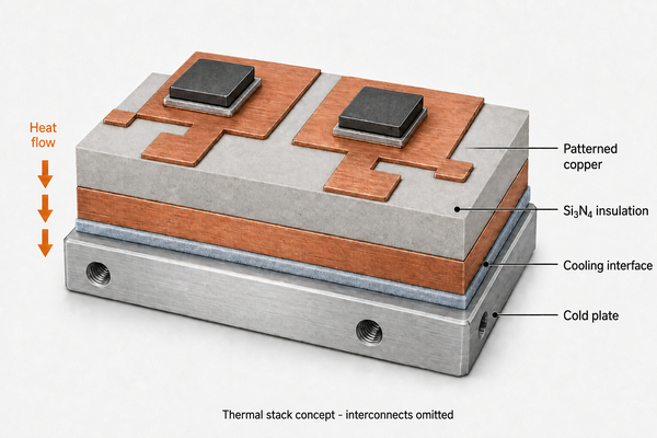
Si3N4 power-module thermal stack concept with semiconductor dies and cooling interface

Traction-Inverter Power Stages

Repeated acceleration and changing load create thermal excursions in the power stage. A Si3N4-based structure can address the combination of copper loading and ceramic crack resistance. For the circuit build, we need the device-pad layout, copper thickness, substrate attachment method and operating temperature range; the module design must also account for interconnect and joint fatigue.

Charger and Industrial-Drive Power Stages

In a charger’s switching bridge or an industrial drive’s power module, sustained losses and switching transients place demands on both heat removal and insulation. Substrate dimensions, conductor separation and the underside mounting surface therefore need to be developed with the cooling and packaging arrangement. Choosing a thinner ceramic solely to reduce thermal resistance can change insulation and mechanical margins.

These are application design scenarios for the circuit substrate, not claims that we manufacture complete traction inverters, chargers or motor drives. The illustration shows the heat-path concept; it is not a customer module or a production photograph.

Circuit Acceptance and Module-Level Validation

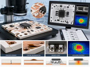
As a silicon nitride substrate manufacturer, we work with you to define acceptance requirements for the fabricated circuit. The inspection plan should address conductor geometry, continuity and isolation, ceramic edge condition, finished dimensions, flatness and surface condition. Joining-interface inspection requirements and suitable methods should be agreed for the selected process.
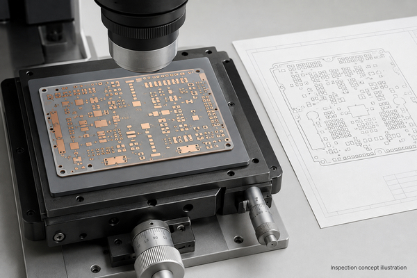
Optical inspection concept for a patterned Si3N4 ceramic circuit substrate

A circuit inspection and a module qualification answer different questions. The first checks whether the substrate meets its drawing and acceptance criteria. Thermal or power cycling, partial-discharge testing where required, and assembled thermal-performance validation establish behavior under the module’s actual operating conditions. An optical image cannot demonstrate those lifetime results.

When comparing silicon nitride manufacturers, distinguish bare-material specifications from the ability to manufacture the required copper circuit. Our role is ceramic circuit fabrication, with DPC or AMB process selection, manufacturability review and project-specific acceptance planning. We do not describe a raw-material datasheet as our own finished-module performance guarantee.

Si3N4 cost depends on material grade, dimensions, copper structure, finish and quantity. We review these together so the quoted construction matches the drawing. Send your circuit artwork, stack-up, attachment requirements and target quantity to sales@bestpcbs.com; our team can review a manufacturable Si3N4 configuration for your power-electronics project.
You may also like

DPC Ceramic PCB
Wednesday, April 1st, 2026

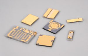
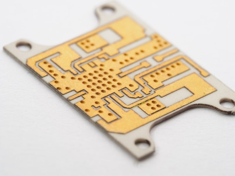
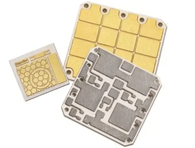
DPC (Direct Plated Copper) technology denotes a special process in which the copper foil and the Al2O3 or AlN (one or both sides) are directly plated under appropriate high temperature.

The super-thin DPC substrate has excellent electrical isolation, high thermal conductivity, fine solderability and high bonding strength. It can be etched like normal FR4 PCB, but has a high current loading capability. Therefore DPC ceramic PCB has become the base materials of construction and interconnection technology of high power semiconductor electronic circuits and also have been the basis for the “Chip On Board” (COB) technology which represent the packaging trend in the future.

Why Choose DPC Ceramic PCB?

DPC ceramic PCB is widely used in high-performance electronic packaging because it provides several practical advantages:

  • Excellent electrical insulation
  • High thermal conductivity
  • Fine line and fine spacing capability
  • Strong copper bonding strength
  • Good solderability for advanced packaging
  • High current carrying capacity
  • Suitable for miniaturized and high-density circuit designs

Another important benefit is that DPC ceramic PCB can be processed in a way similar to standard PCB etching, which gives engineers more design flexibility while maintaining the thermal and mechanical strengths of ceramic materials.

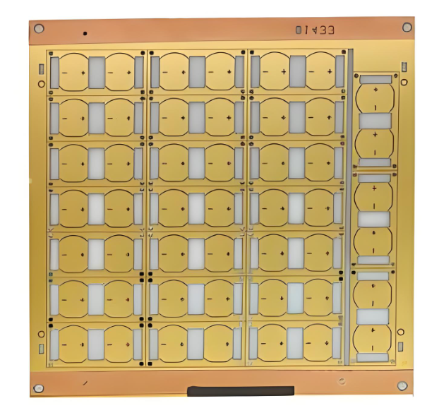
DPC Ceramic PCB

DPC Ceramic PCB

Typical Applications of DPC Ceramic PCB

Because of its structure and performance, DPC ceramic PCB is often used in:

  • High power semiconductor modules
  • LED packaging
  • RF and microwave devices
  • Automotive electronics
  • Power control systems
  • Laser devices
  • Medical electronics
  • Chip on Board (COB) packaging

DPC technology has become an important foundation for modern COB packaging and advanced electronic interconnection, especially in products where heat management and circuit precision are both critical.

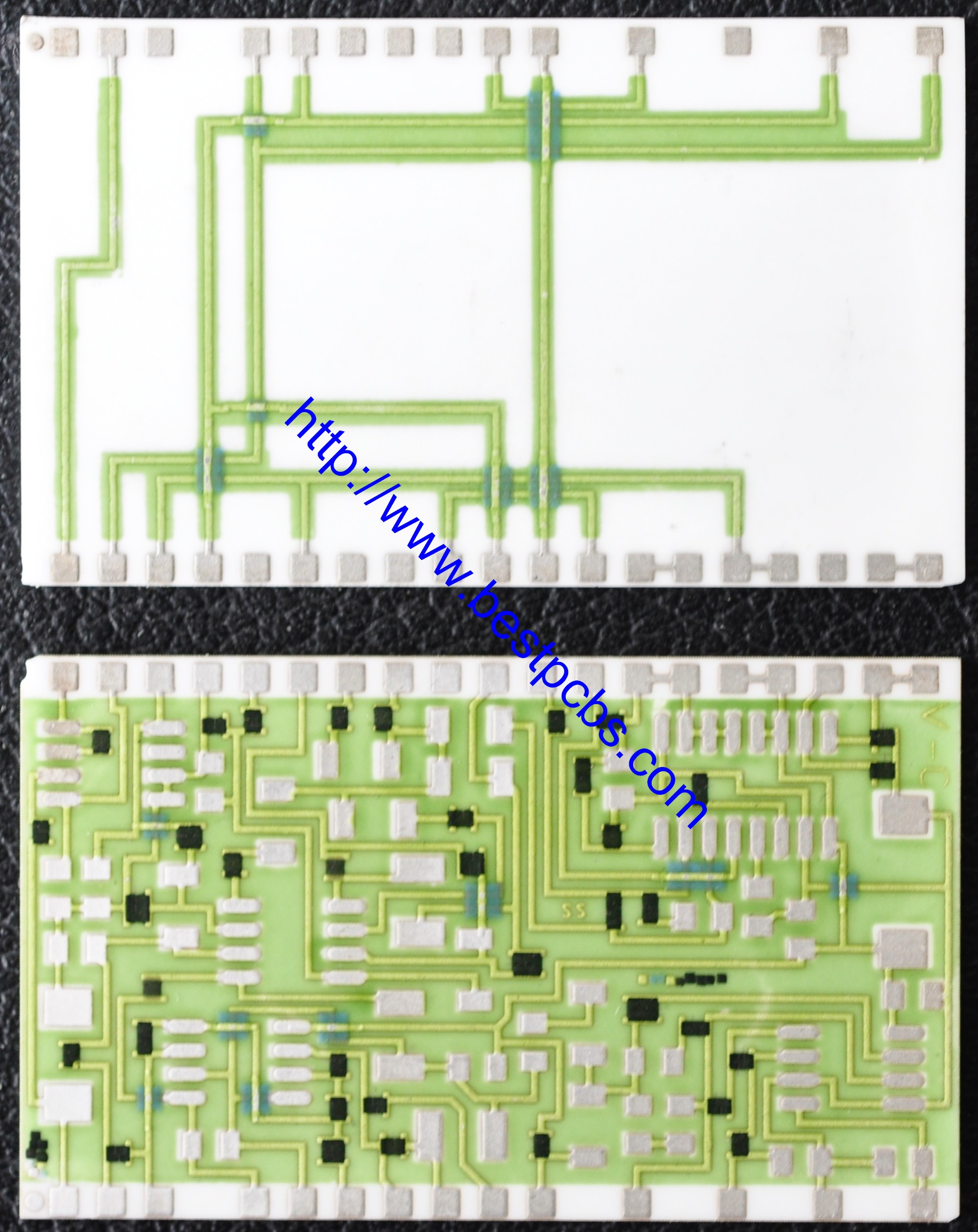
Available DPC Ceramic PCB Samples

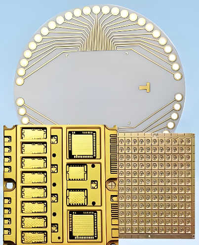
Below are some of our DPC ceramic PCB product examples for reference, you can visit the portal as below to see more product photos:

  • BCD18309 – 2 Layers, 1.5mm Ceramic PCB
  • BCD18372 – 2 Layers, 0.5mm AlN Ceramic PCB
  • BCD19449-B – 2 Layers, 1.0mm, 2oz Ceramic PCB
  • BCD20092– 2 Layers, 0.635mm Ceramic PCB
  • BCD20093 – 2 Layers, 0.635mm Ceramic PCB
  • BCD20108 – 2 Layers, 1.0mm AlN Ceramic PCB
  • BCD20109 – 2 Layers, 1.0mm Al2O3 Ceramic PCB
  • BCD20140 – 2 Layers, 1.0mm AlN Ceramic PCB
  • BCD20162 – 2 Layers, 0.635mm AlN Ceramic PCB
  • BCD20271 – 2 Layers, 0.635mm, 4oz AlN Ceramic PCB
  • BCS20051 – 1 Layer, 0.635mm, 1oz Al2O3 Ceramic PCB
  • BCS20091 – 1 Layer, 1.0mm, 1oz Al2O3 Ceramic PCB
  • BCS20228 – 1 Layer, 0.635mm, 2oz Al2O3 Ceramic PCB
  • BCS20297 – 1 Layer, 0.5mm, 5–7ÎŒm Al2O3 Ceramic PCB

Please contact us today for more information about Ceramic circuit board (Ceramic PCB).

Learn More About Our Ceramic PCB Solutions

We offer a wide range of DPC ceramic circuit boards for customers who need reliable thermal management, precise copper patterns, and stable performance in demanding environments. You are welcome to review our product portal for more sample photos and specifications.

Contact us today to learn more about our ceramic PCB manufacturing capabilities and get support for your project.

You may also like

Ceramic Substrate PCB Manufacturer Design & Prototype| Fast Delivery, Custom Solutions
Monday, March 30th, 2026

Why Choose EBest for Your Ceramic Substrate PCB Needs?

EBest stands as your premier choice for Ceramic Substrate PCB manufacturing and prototyping. We deliver unmatched lead times, rigorous quality control, industry-leading certifications, and comprehensive support throughout your project. Our commitment to excellence ensures your Ceramic Substrate PCB projects are completed efficiently, reliably, and to the highest standards.

  • Fast Delivery: Industry-leading turnaround times for prototypes and mass production, meeting your critical project deadlines.
  • Superior Quality: Precision manufacturing with zero-defect tolerance, ensuring optimal performance and long-term reliability.
  • Certified Excellence: Compliant with ISO 9001, IPC-A-600, and other international quality and safety standards.
  • Expert Support: A dedicated engineering team provides end-to-end technical assistance, from design to delivery.

What is a Ceramic Substrate PCB?

A Ceramic Substrate PCB is a specialized printed circuit board that uses ceramic materials (such as alumina Al₂O₃, aluminum nitride AlN, or silicon nitride Si₃N₄) as its base insulating layer instead of traditional organic materials like FR-4. These boards are engineered to excel in high-temperature, high-power, and high-frequency electronic applications where standard PCBs fail. The ceramic substrate provides exceptional thermal conductivity, electrical insulation, and mechanical stability, making it indispensable for modern, demanding electronics.

Ceramic Substrate PCB

Ceramic Substrate PCB Stackup

LayerMaterialThickness (Typical)Function
Top CopperElectrodeposited Copper1–5 oz (35–175 ÎŒm)Conductive traces, pads, and planes
Ceramic CoreAlumina (Al₂O₃) / Aluminum Nitride (AlN)0.25–2.0 mmInsulation, thermal management, structural support
Bottom CopperElectrodeposited Copper1–5 oz (35–175 ÎŒm)Conductive traces, pads, and planes
Surface FinishENIG / Immersion Silver / OSP0.05–0.5 ÎŒmProtect copper, improve solderability

Note: Multilayer ceramic substrate PCBs (LTCC/HTCC) feature alternating ceramic and conductive layers, typically up to 10–20 layers for high-density integration.

Ceramic Substrate PCB Manufacturing Process

Step 1: Ceramic Substrate Preparation

High-purity ceramic powders (Al₂O₃, AlN) are pressed into green sheets, precisely cut to size, and sintered at ultra-high temperatures (1,600–1,800°C) to form dense, rigid substrates with consistent material properties.

Step 2: Metallization & Circuit Patterning

Copper is bonded to the ceramic surface using advanced processes:

  • DBC (Direct Bonded Copper): Copper foil is fusion-bonded to ceramic at ~1,065°C.
  • DPC (Direct Plated Copper): Copper is electroplated onto a sputtered seed layer for fine-line precision.

Photolithography and etching define the circuit pattern, creating high-resolution traces and pads.

Step 3: Via Formation & Plating

Micro-vias are created using laser drilling for precision. The via walls are metallized through electroplating to establish vertical electrical connections between layers, critical for thermal and signal paths.

Step 4: Surface Treatment & Finishing

The board undergoes surface finishing (ENIG, immersion silver, etc.) to protect the copper circuitry and ensure reliable solderability during component assembly.

Step 5: Testing & Quality Assurance

Each Ceramic Substrate PCB undergoes rigorous electrical testing (continuity, insulation resistance), thermal cycling, and visual inspection to guarantee compliance with specifications and performance standards.

Ceramic Substrate PCB Design Guide

Designing a Ceramic Substrate PCB requires specialized knowledge to overcome inherent material challenges. Key pain points include material brittleness, CTE mismatch with components, thermal management, and fine-line manufacturing constraints. EBest’s engineering team provides expert guidance to navigate these challenges and optimize your design for success.

Key Design Considerations & Solutions

Material Compatibility & CTE Matching

  • Pain Point: A significant CTE mismatch between ceramic (5–7 ppm/°C) and silicon (4.5 ppm/°C) causes thermal stress, leading to solder joint fatigue and substrate cracking.
  • Solution: Select AlN (CTE ~4.5 ppm/°C) for silicon-based high-power devices. Use compliant materials and underfill in assembly to absorb stress.

Thermal Management Optimization

  • Pain Point: Inefficient heat dissipation leads to hotspots and component failure in high-power designs.
  • Solution: Maximize copper thickness in power paths, integrate thermal vias, and use large copper planes for heat spreading. AlN substrates offer 8–10x higher thermal conductivity than alumina.

Mechanical Stress & Fragility

  • Pain Point: Ceramic brittleness causes chipping and cracking during handling, assembly, or thermal cycling.
  • Solution: Avoid sharp corners; use rounded geometries. Design generous tolerances (+/–0.1 mm) and avoid V-cuts. Use robust panelization with thick connecting tabs.

Fine-Line & High-Density Design

  • Pain Point: Achieving fine line widths/spacing (<50 ÎŒm) is challenging with standard processes.
  • Solution: Utilize DPC technology for line widths down to 15 ÎŒm. Collaborate with EBest early for DFM analysis to ensure design manufacturability.

For flawless Ceramic Substrate PCB design, partner with EBest. Our experts provide complimentary DFM reviews and design optimization to ensure your project is built for performance and reliability.
Ceramic Substrate PCB Prototype: Rapid, Reliable, Custom

Prototyping Ceramic Substrate PCBs presents unique hurdles: long lead times, high costs, and difficulty in achieving consistent quality with low volumes. EBest specializes in rapid, high-quality Ceramic Substrate PCB prototyping, eliminating these barriers and accelerating your product development cycle.

Prototype Challenges & Our Solutions

Long Lead Times for Custom Prototypes

  • Challenge: Traditional ceramic PCB prototyping can take weeks, delaying product validation.
  • Solution: EBest offers rapid prototype services with industry-leading turnaround times, getting your boards in hand quickly.

High Cost for Low-Volume Runs

  • Challenge: High tooling and setup costs make small-batch prototyping prohibitively expensive.
  • Solution: We maintain flexible manufacturing lines optimized for low-volume, high-mix production, keeping prototype costs competitive.

Inconsistent Prototype Quality

  • Challenge: Achieving the same material and process quality in prototypes as in mass production is difficult.
  • Solution: Our prototypes use the exact same materials and production processes as full-scale manufacturing, ensuring reliable performance data.

Limited Design Iteration

  • Challenge: Cost and time constraints limit the number of design iterations possible.
  • Solution: Our efficient prototyping process allows for multiple design iterations, enabling you to refine and perfect your design before full production.

Trust EBest for your Ceramic Substrate PCB prototyping needs. We deliver fast, affordable, and production-quality prototypes to validate your design and accelerate your time-to-market.

How to Choose Ceramic Substrate PCB Raw Materials

Selecting the right ceramic material is critical for balancing performance, cost, and application suitability. The table below compares the most common materials:

MaterialThermal Conductivity (W/m·K)CTE (ppm/°C)Dielectric Constant (Δr)Key Applications
Alumina (96% Al₂O₃)20–25~7.09.5Consumer electronics, industrial control, LED lighting
Alumina (99% Al₂O₃)28–30~7.09.8Automotive electronics, medical devices, telecom
Aluminum Nitride (AlN)170–230~4.58.8High-power semiconductors, RF, EV power modules
Silicon Nitride (Si₃N₄)80–100~3.27.8Automotive, aerospace, high-reliability industrial

Ceramic Substrate PCB Applications

Ceramic Substrate PCBs are the backbone of high-performance electronics across critical industries, enabling innovation where thermal, electrical, and reliability demands are extreme.

Automotive Electronics

Ceramic Substrate PCBs are essential in electric vehicle (EV) powertrains, including IGBT modules, on-board chargers (OBC), and LED headlight drivers. They withstand extreme under-hood temperatures (-40°C to 150°C) and provide superior thermal management for high-voltage, high-power systems.

Communication & 5G Infrastructure

In 5G base stations, RF power amplifiers, and microwave systems, Ceramic Substrate PCBs (especially AlN) offer low dielectric loss and excellent thermal stability, ensuring signal integrity and efficient heat dissipation for high-frequency, high-power operation.

Industrial Automation & Power Electronics

Used in variable-frequency drives (VFDs), servo controls, and power supplies, these boards handle high power densities and harsh industrial environments. Their excellent thermal conductivity and mechanical strength ensure reliable operation in continuous-duty applications.

Medical Devices

Ceramic Substrate PCBs are used in precision medical equipment like ultrasound systems, patient monitors, and surgical lasers. They offer biocompatibility, high electrical insulation, and the ability to withstand repeated sterilization cycles, meeting strict medical device standards.

What Are the Key Advantages of Ceramic Substrate PCB Over FR4?

Ceramic Substrate PCBs offer transformative advantages over traditional FR-4 PCBs, particularly in high-performance applications. Key benefits include:

  • Superior Thermal Conductivity: Up to 1,000x higher than FR-4, enabling efficient heat dissipation.
  • Excellent Electrical Insulation: High dielectric strength prevents short circuits in high-voltage applications.
  • Extreme Temperature Resistance: Operates reliably from -50°C to over 350°C.
  • Mechanical Stability: High rigidity and resistance to warping under thermal stress.
  • Chemical Inertness: Resistant to most chemicals, ideal for harsh environments.

How Does Thermal Conductivity Impact Ceramic Substrate PCB Performance?

Thermal conductivity is the defining performance metric for Ceramic Substrate PCBs. It directly determines the board’s ability to dissipate heat generated by power components. Higher thermal conductivity (e.g., AlN at 200 W/m·K vs. alumina at 25 W/m·K) allows for:

  • Higher power density designs in smaller form factors.
  • Lower component operating temperatures, significantly increasing reliability and lifespan.
  • Elimination of bulky heat sinks, enabling more compact and efficient product designs.

What Are the Common Failure Modes in Ceramic Substrate PCBs?

The primary failure modes stem from thermal and mechanical stress:

  • Thermal Fatigue: CTE mismatch causes cyclic stress, leading to solder joint cracking or substrate delamination.
  • Mechanical Fracture: Brittleness leads to cracking from shock, vibration, or improper handling.
  • Metallization Degradation: Oxidation or poor adhesion of the copper layer causes open circuits.
  • Thermal Runaway: Inadequate heat dissipation leads to overheating and catastrophic failure.

Can Ceramic Substrate PCBs Be Used for High-Frequency Applications?

Absolutely. Ceramic Substrate PCBs, especially AlN and high-purity alumina, are ideal for high-frequency (RF/microwave) applications. They offer:

  • Low Dielectric Loss (tan ÎŽ): Minimizes signal attenuation and power loss.
  • Stable Dielectric Constant: Ensures consistent signal propagation across temperature variations.
  • Excellent High-Frequency Performance: Supports frequencies up to mmWave bands for 5G and radar systems.

What Is the Difference Between DBC and DPC Ceramic Substrate PCB?

DBC (Direct Bonded Copper) and DPC (Direct Plated Copper) are the two primary manufacturing technologies:

  • DBC: Copper foil is fusion-bonded to ceramic at high temperature. It is best for thick copper (up to 10 oz) and high-power applications. It offers excellent thermal performance but limited line resolution (~100 ÎŒm).
  • DPC: Copper is electroplated onto a sputtered seed layer. It enables ultra-fine line widths (<15 ÎŒm) for high-density, high-frequency designs. It is ideal for complex, miniaturized circuits.

Ceramic Substrate PCB FAQ

Q1: What is the maximum operating temperature for a Ceramic Substrate PCB?

A1: Ceramic Substrate PCBs can reliably operate at continuous temperatures up to 350°C, with short-term peaks exceeding 500°C—far exceeding the limits of FR-4.

Q2: Can you manufacture flexible Ceramic Substrate PCBs?

A2: While inherently rigid, specialized ceramic composites and LTCC (Low-Temperature Co-fired Ceramic) technologies can produce semi-flexible or 3D-shaped Ceramic Substrate PCBs for specific applications.

Q3: What is the minimum line width/spacing achievable?

A3: Using DPC technology, EBest can achieve line widths and spacing as fine as 15 ÎŒm, enabling high-density circuit designs.

Q4: Are Ceramic Substrate PCBs suitable for mass production?

A4: Yes. EBest operates automated production lines capable of high-volume, consistent manufacturing of Ceramic Substrate PCBs for industrial and automotive applications.

Q5: How do I get a quote for my Ceramic Substrate PCB project?

A5: Contact our sales team with your Gerber files, BOM, layer stackup, quantity, and target delivery date. We provide detailed, competitive quotes quickly.

Q6: What surface finishes are available for Ceramic Substrate PCBs?

A6: We offer ENIG (Electroless Nickel Immersion Gold), immersion silver, and OSP (Organic Solderability Preservative) to meet various assembly and reliability requirements.

Q7: Can you assemble components on Ceramic Substrate PCBs?

A7: Yes, EBest provides full turnkey services, including high-precision SMT and through-hole component assembly for Ceramic Substrate PCBs.

Ready to Start Your Ceramic Substrate PCB Project?

EBest is your trusted partner for all Ceramic Substrate PCB design, prototyping, and manufacturing needs. With our technical expertise, fast delivery, and commitment to quality, we ensure your project succeeds. Contact us today to discuss your requirements and get a free quote.

Email: sales@bestpcbs.com

You may also like

Design and Application of PVD in DPC Manufacturing Process
Monday, July 29th, 2024

With the increasing demand of electronic devices working in high temperature environment, DPC (Direct-Plated Copper) ceramic PCB has been widely used as a heat dissipation material with strong high temperature stability and high thermal conductivity. This paper discusses the design and application of DPC ceramic substrate from the aspects of material, structure and technology.

Material Selection of DPC Ceramic PCB

It is very important to select ceramic substrate with good high temperature stability and high thermal conductivity. Commonly used ceramic materials are Al2O3, AlN, Si3N4 and so on. Taking Al2O3 as an example, its thermal conductivity is as high as 24~30W/(m·K), and the coefficient of thermal expansion is about 8.2×10^-6/℃, which is similar to the coefficient of thermal expansion of most chips. The ceramic layer on the surface of the substrate should be smooth and uniform, and have good adhesion, oxidation resistance, wear resistance and corrosion resistance.

Design and Application of PVD in DPC Manufacturing Process

The heat dissipation performance of DPC ceramic substrate is one of the key factors affecting its work in high temperature environment. In order to test the heat dissipation performance of DPC ceramic substrate, thermocouple temperature measurement, infrared temperature measurement, thermal imager and other testing methods can be used. The experimental results show that the DPC ceramic substrate has good heat dissipation performance and can effectively heat dissipation and reduce the influence of temperature on electronic devices.

DPC Ceramic PCB Structure Design

The structure design of DPC ceramic substrate includes the thickness of copper foil, the size of aperture, the layout of copper foil and the thickness of ceramic substrate. The choice of copper foil thickness should be determined according to heat dissipation requirements and chip power density and other parameters.

There are two layout methods of copper foil, one is fully plated surface; The other is local copper, that is, only the copper foil is laid in the area around the chip. The local copper laying method can reduce the copper foil area and reduce the cost, but the adhesion between the copper foil and the substrate needs to be higher. The thickness of the ceramic substrate also needs to be selected according to the specific application requirements.

PVD Process of DPC Ceramic PCB

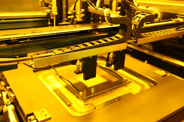
Direct Plating Copper (DPC) is a ceramic circuit processing technology developed on the basis of ceramic film processing. In this process, the copper metal composite layer is sputtered on the ceramic substrate by vacuum coating, and then the circuit is made by re-exposure, development, etching and film removal with the photoresistance of yellow light microshadow. Finally, the thickness of the circuit is increased by electroplating/electroless deposition, and the metallized circuit is made after the photoresistance is removed.

The process is the process of vaporizing metal materials (titanium and copper) into molecules and then forming a metal film on the surface of a ceramic substrate. The main process includes cleaning the surface of the substrate, heat treatment of the ceramic substrate, preparation of the target of metal materials, DPC of the target, measurement of film thickness and surface treatment. Among them, heat treatment can improve the thermal stability and adhesion of the ceramic substrate, and ensure that the covered copper foil will not peel off in high temperature environment.

DPC ceramic substrate small size, precision structure, high reliability requirements, complex process flow, fine production process, belongs to technology-intensive industries, with high technical barriers. Its production process mainly involves drilling, magnetron sputtering, chemical copper deposition, copper plating, solder resistance printing, chemical silver/chemical gold deposition and other main processes

Application of DPC Ceramic PCB

a. VCSEL package

    The power density of VCSEL is very high, and the DPC ceramic circuit board has a high thermal expansion coefficient matching with VCSEL, so as to solve the stress problem caused by the mismatch of thermal expansion between chip and substrate. The DPC ceramic circuit board makes the metal edge closely combined with the ceramic substrate, avoiding the additional paste process, coordination accuracy and other problems in the later assembly process, as well as the reliability problems caused by the aging of the glue. The ceramic circuit board of DPC film technology almost meets the packaging requirements of VCSEL.

    Design and Application of PVD in DPC Manufacturing Process

    b. IGBT package

    The insulated gate bipolar transistor has become the mainstream of the development of power semiconductor devices due to its high input impedance, fast switching speed, low on-state current and high blocking voltage. Its applications are as small as frequency conversion air conditioning, silent refrigerator, washing machine, induction cooker, microwave oven and other household appliances, and as large as electric locomotive traction system. Due to the high output power and high heat output of IGBT, heat dissipation is the key for IGBT packaging. At present, the DPC ceramic substrate is mainly used for IGBT packaging, because the DPC ceramic substrate has the characteristics of large metal layer thickness, high bonding strength (good thermal impact) and so on.

    c. LED package

    Throughout the development of LED technology, the power density continues to improve, and the requirements for bracket heat dissipation are becoming higher and higher. DPC ceramic substrate has high insulation, high thermal conductivity and heat resistance, low expansion and other characteristics, especially the use of through hole interconnection technology, well meet the LED flip, eutectic, COB (chip on board), CSP (chip scale package), WLP (wafer package) packaging needs, suitable for medium and high power LED packaging.

    In conclusion, the design and application of DPC copper-coated ceramic substrate need to consider many factors, and a lot of experiments and data analysis are required. The performance and reliability of DPC ceramic substrate at high temperature can be improved by selecting suitable materials and designing reasonable structure and process, and the high temperature application of microelectronic devices can be guaranteed.

    The advent of DPC ceramic substrate products opens the development of heat dissipation application industry. Due to the heat dissipation characteristics of the ceramic substrate, it has the advantages of high heat dissipation, low thermal resistance, long life and voltage resistance. With the improvement of production technology and equipment, the rationalization of product prices is accelerated, and the application field of LED industry is expanded.

    You may also like

    How does a DPC Ceramic PCB Manufactured?
    Saturday, July 6th, 2024

    Direct Plating Copper (DPC) is a ceramic circuit board developed on the basis of ceramic film processing. Aluminum nitride/alumina ceramic is used as the substrate of the circuit, and the composite metal layer on the surface of the substrate is sputtered, and the circuit is formed by electroplating and lithography. Its basic processes are:

    • Incoming Quality Control (IQC)

    The process begins with the inspection of raw materials to ensure they meet strict quality standards. This step involves checking ceramic substrates for physical defects such as cracks, chips, or surface irregularities, and verifying material properties like thermal conductivity and dielectric strength. Advanced equipment such as microscopes and X-ray fluorescence (XRF) analyzers are used for thorough inspection, ensuring only the best materials proceed to the next stage.

    • Laser Drilling

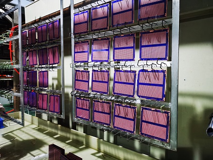
    Before laser drilling, a water-soluble, food-grade substrate pigment is brushed onto the ceramic substrate to reduce reflectivity and enhance laser drilling effectiveness. After drying in an oven, a laser drilling machine is used to drill through the substrate, creating pathways for connections between the upper and lower surfaces. Depending on the ceramic material, different laser wavelengths such as infrared, green light, ultraviolet, or CO2 are used to burn away the material with each laser pulse.

    How does a DPC Ceramic PCB Manufactured?
    • Laser Marking

    Laser marking involves using a laser marking machine to engrave product QR codes onto the ceramic substrate. This step ensures precise and permanent identification marks on the PCB.

    • Ultrasonic Cleaning

    After laser drilling and marking, the substrates are cleaned to remove any attached particles or residues. This involves coarse and fine debris removal using ultrasonic cleaning, followed by water washing to eliminate any remaining particles. The cleaned substrates undergo micro-etching to roughen the surface, enhancing the effectiveness of subsequent magnetron sputtering, and are then dried to remove surface moisture.

    • Magnetron Sputtering

    In the magnetron sputtering process, a high-vacuum chamber is used to ionize argon gas, producing an ion stream that bombards a target cathode. This causes atoms of the target material to be ejected and deposited as a thin film on the ceramic substrate. Pre-sputtering treatments such as dust removal, degreasing, and slow pulling are conducted to ensure optimal results.

    • Chemical Copper Plating

    Chemical copper plating thickens the copper layer, improving the conductivity of the vias and ensuring better adhesion with the sputtered copper layer. This catalytic redox reaction involves pre-treatment steps like degreasing, micro-etching, pre-immersion, activation, and acceleration to ensure proper copper deposition.

    • Full-Panel Electroplating

    Full-panel electroplating increases the thickness of the copper layer. This involves processes such as degreasing, micro-etching, acid washing, copper plating, and stripping excess copper from the fixtures. The copper plating uses copper balls as anodes and an electrolyte solution of CuSO4 and H2SO4, with the primary reaction being Cu2+ + 2e- → Cu.

    • Grinding, Laminating, Exposure, and Developing

    Post electroplating, the copper layer is prepared for patterning. This includes acid washing to remove oxides, grinding to roughen and clean the surface, laminating with a photoresist dry film, UV exposure through a photomask to create the desired pattern, and developing to dissolve unexposed areas, leaving behind the patterned photoresist.

    How does a DPC Ceramic PCB Manufactured?

    • Pattern Plating (Electroplating Copper)

    The exposed and developed areas of the substrate where the circuit pattern is defined undergo further copper electroplating to thicken the circuit traces.

    How does a DPC Ceramic PCB Manufactured?
    • Etching and Stripping

    Unwanted copper and dry film are removed through etching, stripping away excess copper deposited in previous steps. This includes rough grinding, film stripping, copper etching, and titanium etching, ensuring only the desired circuit pattern remains.

    • Annealing

    The ceramic boards are annealed in a furnace to relieve stresses introduced during electroplating, enhancing the ductility and toughness of the copper layer and ensuring dense copper grain packing.

    • Belt Grinding

    Post-annealing, the substrate surface may have an oxide layer and rough texture. Belt grinding is used to remove these oxides and smoothen the surface, ensuring the quality of subsequent gold or silver surface treatments.

    • Flying Probe Testing

    High-speed flying probe testers check for continuity and shorts in the vias and circuit traces, ensuring electrical integrity.

    • Sandblasting Before Solder Mask

    Prior to solder mask application, the substrate undergoes sandblasting to roughen and clean the surface, removing oxides and contaminants. This includes acid washing, sandblasting, and micro-etching.

    • Solder Mask Printing

    Solder mask is printed on areas of the PCB that do not require soldering, protecting the circuits during soldering and assembly. Screen printing applies solder mask ink, which is then UV-cured and developed to remove unexposed areas.

    • Sandblasting After Solder Mask

    After solder mask application, exposed areas that need surface treatments undergo sandblasting to roughen the surface and remove oxides, preparing for gold or silver plating.

    • Surface Treatment

    Surface treatments like electroless or electrolytic plating of gold, silver, or other metals are applied to the solder pads, enhancing solderability and preventing oxidation.

    • Laser Cutting

    Laser cutting equipment precisely cuts the finished PCBs from the manufacturing panel, ensuring accurate dimensions and clean edges.

    • Testing

    Various testing equipment, including thickness gauges, Automated Optical Inspection (AOI) machines, and ultrasonic scanning microscopes, are used to inspect the PCBs’ performance and appearance, ensuring they meet quality standards.

    • Packaging and Shipping

    Finally, the PCBs are vacuum-packed using packaging machines to protect them during transport. They are then stored and shipped to customers, ensuring they arrive in perfect condition.

    Above is the all the processes of DPC muanufacturing. If you are interested in process of other PCBs, welcome to contact us.

    You may also like