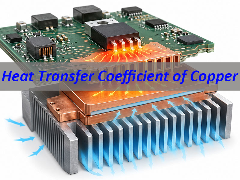
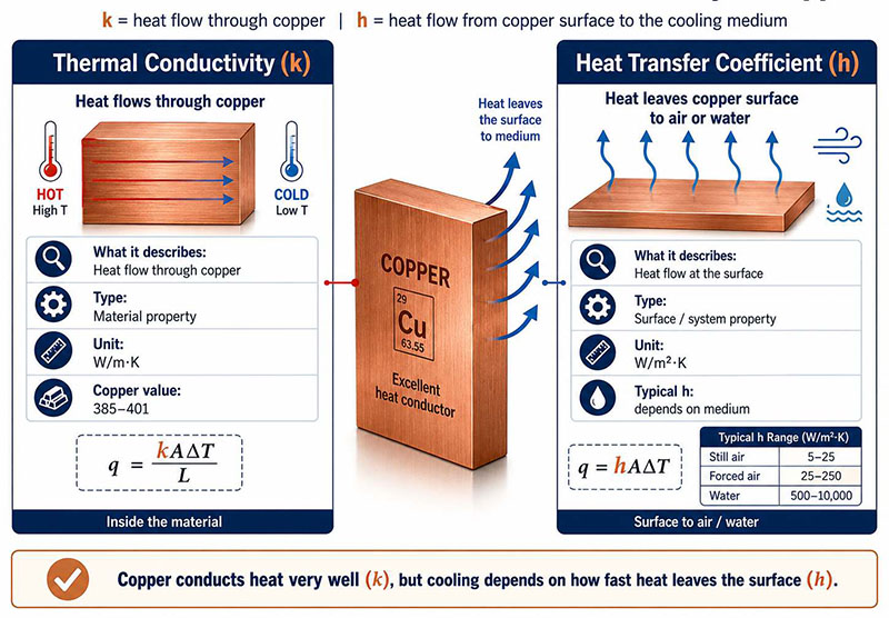
Heat transfer coefficient of copper is an important concept in thermal management, especially for heat sinks, copper core PCBs, heavy copper PCBs, copper inlay boards, PCB bus bars, heat pipes, cold plates, vapor chambers, and power electronics assemblies. Many people search for this term expecting one fixed value, just like the thermal conductivity of copper. In reality, these two terms are different. Copper has a high thermal conductivity, usually around 385–401 W/m·K for pure copper at room temperature, which describes how well heat travels through copper itself.
The heat transfer coefficient, often represented by h, describes how efficiently heat moves from a copper surface to a surrounding medium, such as air, water, oil, steam, or another contact surface. It is usually measured in W/m²·K and depends on cooling medium, airflow or liquid flow, surface area, surface finish, temperature difference, contact quality, and the full thermal path. For PCB, PCBA, heat sink, LED module assembly, EV charger, AI server power board, and industrial power electronics design, this distinction is important: copper can spread heat very well, but the heat still needs a real exit path.
What Is the Heat Transfer Coefficient of Copper?
The heat transfer coefficient of copper describes the rate at which heat moves between a copper surface and its surrounding environment. In heat transfer calculations, it is usually written as h.
The basic heat transfer equation is:
Q = h × A × ΔT
Where:
| Symbol | Meaning |
|---|---|
| Q | Heat transfer rate |
| h | Heat transfer coefficient |
| A | Heat transfer surface area |
| ΔT | Temperature difference between the copper surface and the surrounding medium |
This formula shows that heat transfer is not controlled by copper alone. Even if copper conducts heat quickly inside the material, the heat must still leave the copper surface.
For example, imagine the same copper plate used in three different conditions:
| Copper Condition | Heat Transfer Result |
|---|---|
| Copper plate in still air | Heat leaves slowly |
| Copper plate with fan airflow | Heat leaves faster |
| Copper plate cooled by flowing water | Heat leaves much faster |
The copper material is the same in all three cases. What changes is the cooling environment. That is why the heat transfer coefficient must always be discussed together with the actual working condition.
In simple terms:
Copper helps heat spread. The surrounding medium decides how fast heat leaves.
Is the Heat Transfer Coefficient of Copper a Fixed Value?
No. The heat transfer coefficient of copper is not a fixed material value. This is the key point to understand before using it in thermal design. Copper thermal conductivity is a material property, while the heat transfer coefficient is a surface and system property.
Pure copper has high thermal conductivity because free electrons can carry thermal energy efficiently through its metallic structure. That is why copper is widely used in heat spreaders, heat pipes, cold plates, copper base PCBs, and high-current conductive parts. However, the h value depends on how heat leaves the copper surface, not only on the copper itself.
| Copper Condition | Heat Transfer Result |
|---|---|
| Still air | Low |
| Forced airflow | Higher |
| Flowing water | Much higher |
| Copper tube | Flow-dependent |
| Poor contact | Limited |
| Good contact | Improved |
For example, a copper heat sink in still air may have limited cooling performance because air removes heat slowly. With stronger airflow, heat removal improves because moving air reduces the warm boundary layer near the copper surface. A copper cold plate with flowing water can transfer heat much more effectively than air cooling. A copper tube in a heat exchanger also depends on flow speed, tube diameter, wall thickness, and fouling.
So the better engineering question is not simply “What is the heat transfer coefficient of copper?” A more accurate question is: What is the heat transfer coefficient of this copper surface under this cooling condition?
This small change makes the answer more practical. It helps engineers evaluate copper parts based on real working conditions instead of treating copper as if it has one universal h value.
What Is the Unit of Heat Transfer Coefficient of Copper?
The standard unit of heat transfer coefficient is:
W/m²·K
It can also be written as:
W/(m²·K)
This means watts of heat transferred per square meter of surface area for every one kelvin of temperature difference.
This unit is different from the unit used for copper thermal conductivity.
| Parameter | Symbol | Unit | What It Describes |
|---|---|---|---|
| Thermal conductivity of copper | k | W/m·K | Heat conduction through copper |
| Heat transfer coefficient | h | W/m²·K | Heat exchange from surface to fluid |
| Overall heat transfer coefficient | U | W/m²·K | Total heat transfer through a full system |
This distinction is useful because many users confuse these values.
For example, copper thermal conductivity may be around 401 W/m·K, but that does not mean the heat transfer coefficient of copper is 401 W/m²·K. The first value describes conduction through copper. The second type of value describes convection or surface heat exchange.
In PCB thermal design, both values matter. Copper thermal conductivity helps heat move through copper traces, planes, coins, or cores. The heat transfer coefficient affects how heat leaves the board through air, a heat sink, a housing, or a liquid cooling structure.
What Is the Difference Between Heat Transfer Coefficient and Thermal Conductivity of Copper?
Thermal conductivity and heat transfer coefficient are closely related, but they describe different stages of heat movement.
Thermal conductivity of copper answers this question:
How well does heat move through copper?
Heat transfer coefficient of copper answers this question:
How well does heat move from the copper surface to air, water, or another surrounding medium?
A practical example is a copper heat sink. The copper base spreads heat quickly from a hot component. This reduces local hot spots. But the heat still needs to move from the copper surface into the surrounding air. If airflow is weak, the copper heat sink may still run hot.
Another example is a copper core PCB. The copper core can spread heat from LEDs, MOSFETs, power ICs, or charging modules. But if the board does not have good contact with a housing or heat sink, the heat may remain inside the assembly.
So thermal design has two parts:
| Heat Transfer Stage | Main Design Focus |
|---|---|
| Heat spreading inside copper | Copper thickness, copper area, copper purity, copper path |
| Heat removal from copper surface | Airflow, water flow, surface area, heat sink, housing contact |
This is why high copper thermal conductivity alone does not guarantee low operating temperature. A good design must include a complete thermal path.
For PCBs, this means engineers should review copper thickness, copper plane area, via structure, dielectric thermal conductivity, component placement, soldering quality, surface finish, housing contact, and airflow path together.
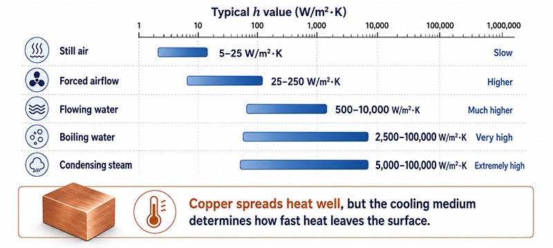
What Are Typical Heat Transfer Coefficient Values for Copper in Air and Water?
Copper does not have one fixed h value, but engineers often use typical ranges based on the cooling condition. These values are general reference ranges. Actual values should be verified by thermal simulation, testing, or project-specific calculation.
| Cooling Condition | Typical Heat Transfer Coefficient Range |
|---|---|
| Natural convection in air | 5–25 W/m²·K |
| Forced convection in air | 25–250 W/m²·K |
| Water cooling | 500–10,000 W/m²·K |
| Boiling water or phase-change cooling | 2,500–100,000 W/m²·K |
| Condensing steam | 5,000–100,000 W/m²·K |
These ranges explain why cooling method matters so much.
A copper plate in still air may not remove heat quickly, even though copper itself has excellent thermal conductivity. If a fan is added, the warm boundary layer near the copper surface becomes thinner, and heat leaves faster. If water is used as the cooling medium, heat removal can increase dramatically.
This is why high-power systems often use copper cold plates, copper tubes, heat pipes, or vapor chambers.
For PCB applications, air cooling may be enough for moderate power designs. For high-power LED modules, EV chargers, laser drivers, AI server power boards, or inverter modules, the design may require metal base PCBs, copper inlay, heavy copper, heat sinks, or liquid cooling assistance.
The key point is simple:
The copper part spreads heat. The cooling method removes heat. Both must work together.
What Factors Affect the Heat Transfer Coefficient of Copper?
Several factors influence the heat transfer coefficient of copper in real applications. Understanding these factors helps engineers avoid thermal design mistakes.
Cooling Medium
- Air, water, oil, and steam have different heat transfer behavior.
- Air cooling is simple, clean, and low-cost, but its heat transfer coefficient is usually lower. Water cooling provides much stronger heat removal and is often used in high-power electronics, server cooling, EV charging, laser systems, and industrial power modules.
- Oil cooling may be used in transformers or special power systems because it can offer insulation and stable thermal behavior. Steam condensation and boiling systems can provide very high heat transfer, but they require more complex design control.
Flow Speed
- Flow speed has a major effect on h value. Still air creates a thick thermal boundary layer around the copper surface, which limits heat removal. Moving air reduces this layer and improves cooling.
- The same logic applies to liquid cooling. Faster water flow usually improves heat transfer, but it also increases pressure drop and pump requirements. A practical design must balance thermal performance, noise, pressure loss, reliability, and cost.
Surface Area
- A larger surface area allows more heat to leave. This is why heat sinks use fins. It is also why copper tubes, copper coils, and cold plates are shaped to increase contact area with air or liquid.
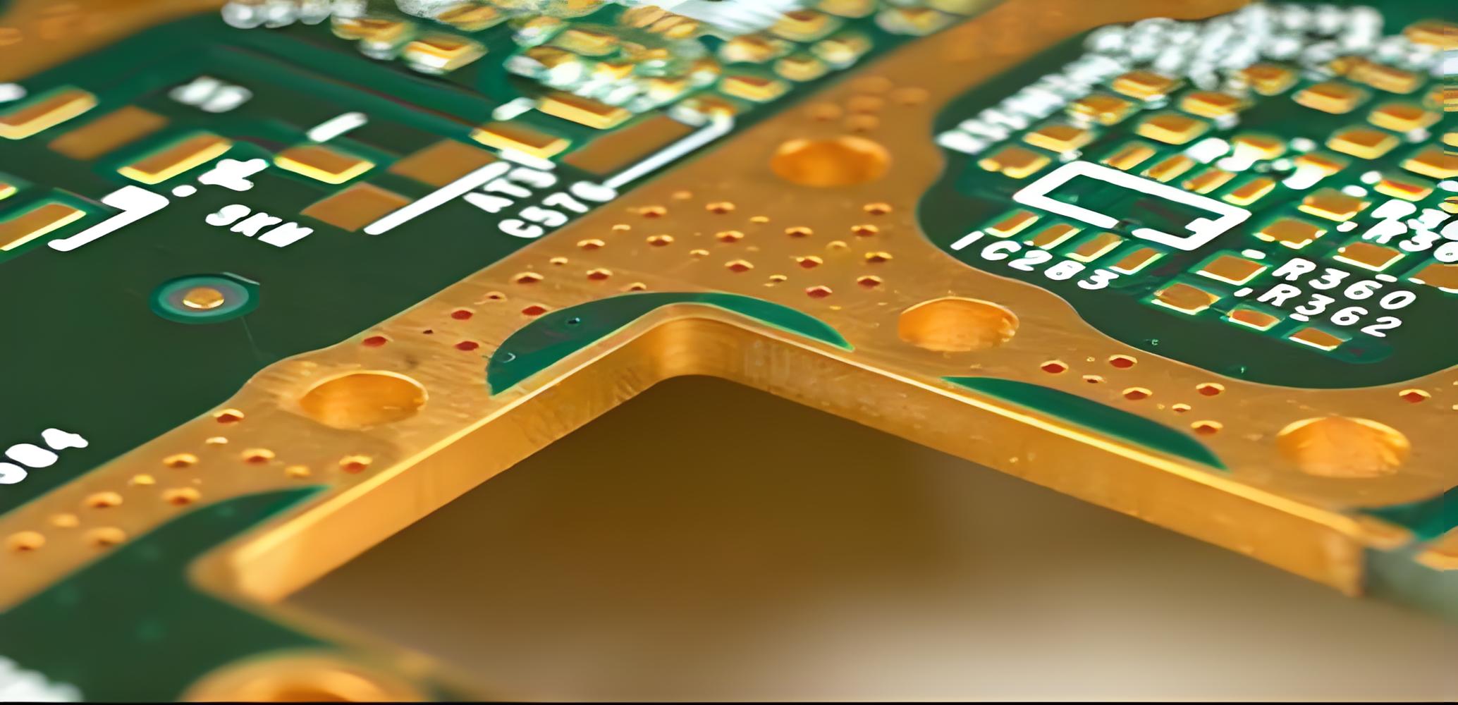
- In PCB design, copper planes, thermal vias, exposed copper pads, copper coins, copper inlays, and metal bases can increase the useful heat spreading area.
- However, more copper area only helps when the heat has a real exit path. A large copper plane inside a sealed product may spread heat, but the product can still overheat if the enclosure cannot release that heat.
Surface Condition
- Copper surface condition also matters. Oxidation, roughness, plating, solder mask, contamination, and coating can change practical heat transfer.
- For example, exposed copper may exchange heat differently from copper covered by solder mask. Nickel, tin, silver, ENIG, OSP, or other finishes may also influence surface contact, oxidation resistance, and assembly behavior.
- In PCB production, surface finish is not chosen only for thermal reasons. It also affects solderability, shelf life, wire bonding, contact reliability, and cost.
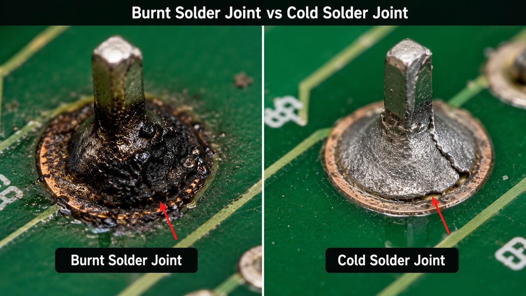
Contact Resistance
- When copper touches another material, the contact interface can become a thermal bottleneck. Air gaps, uneven pressure, poor soldering, weak thermal interface material, and rough surfaces can all increase contact resistance.
- This is common in PCBA thermal issues. The copper may be thick enough, but the heat still cannot pass efficiently into the heat sink or metal housing.
Geometry
- Copper geometry affects heat transfer. A copper plate, pipe, tube, rod, wire, coil, heat pipe, and copper coin all behave differently.
- For example, the heat transfer coefficient of a copper tube depends on tube diameter, wall thickness, fluid velocity, internal surface condition, external cooling medium, and temperature difference. It cannot be judged only by the copper material.
- In PCB design, geometry also matters. A short and wide copper path usually performs better than a long and narrow heat path. Thermal vias placed close to the heat source are usually more effective than vias placed far away.
How Does Copper Compare With Aluminum, Stainless Steel, and Other Metals?
Copper is one of the most practical metals for thermal design. Silver has higher thermal conductivity, but copper is more widely used because it offers a better balance of performance, cost, availability, machinability, and electrical conductivity.
| Material | Approximate Thermal Conductivity | Thermal Design Comment |
|---|---|---|
| Silver | ~429 W/m·K | Excellent conductivity, but expensive |
| Copper | ~385–401 W/m·K | Strong heat spreading and electrical conduction |
| Aluminum | ~205–237 W/m·K | Lightweight and cost-effective |
| Brass | ~80–120 W/m·K | Better mechanical/corrosion properties than pure copper, lower heat transfer |
| Stainless steel | ~14–16 W/m·K | Strong and corrosion-resistant, but poor thermal conductor |
Copper usually performs better than aluminum when fast heat spreading is required. This is useful when heat is concentrated in a small area, such as under a power IC, MOSFET, IGBT, LED chip, or laser diode.
Aluminum has lower thermal conductivity than copper, but it is lighter and more cost-effective. That is why aluminum heat sinks and aluminum PCBs are widely used in LED lighting, consumer electronics, automotive modules, and industrial control products.
Stainless steel is not usually selected for heat spreading. It is used when strength, corrosion resistance, or mechanical stability is more important than heat transfer.
The best material depends on the application:
| Application Need | Better Material Choice |
|---|---|
| Highest practical heat spreading | Copper |
| Lightweight heat sink | Aluminum |
| High current and heat spreading together | Copper |
| Low-cost LED thermal substrate | Aluminum PCB |
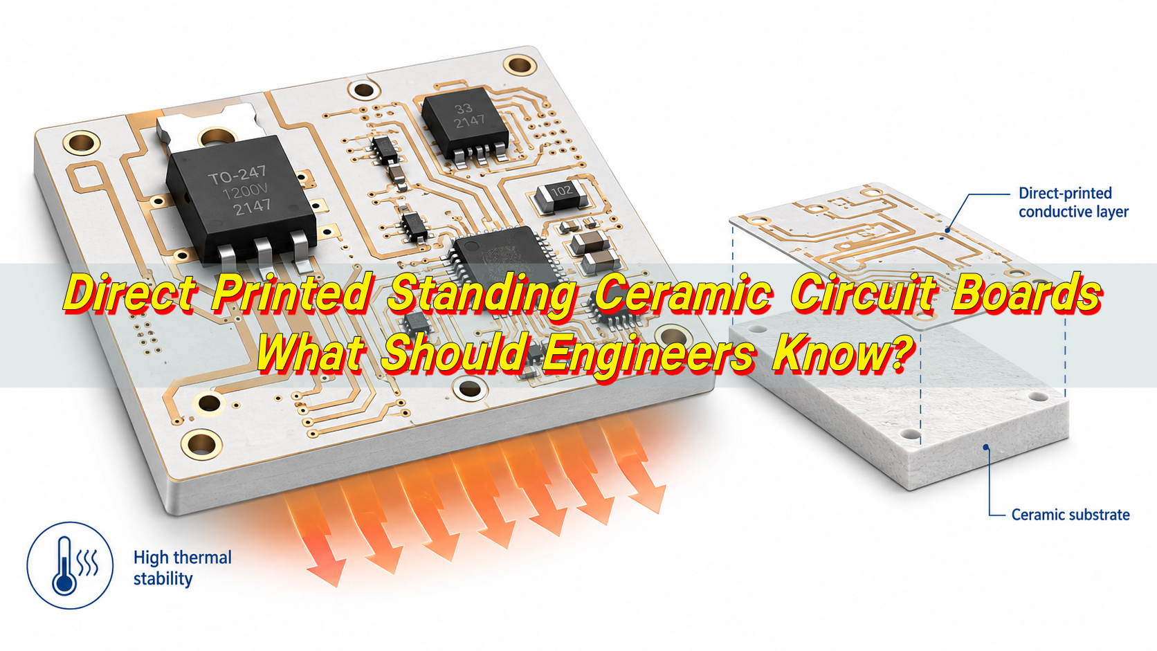
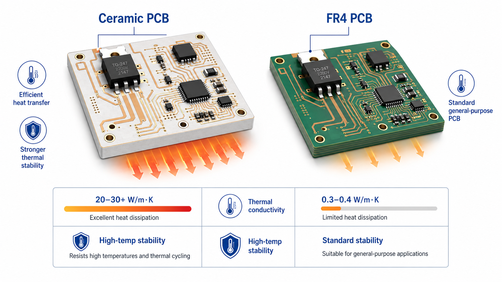
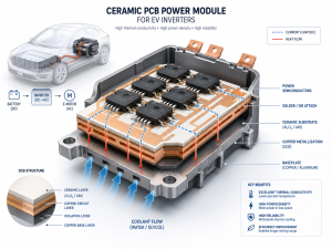
| Electrical insulation plus high thermal path | Ceramic PCB |
| Corrosion-resistant structure | Stainless steel |
| Compact high-power module | Copper core PCB or copper inlay PCB |
For many real products, the best solution is not a single material. A thermal design may combine copper for heat spreading, aluminum for large fin area, ceramic for insulation, and thermal interface material for contact improvement.
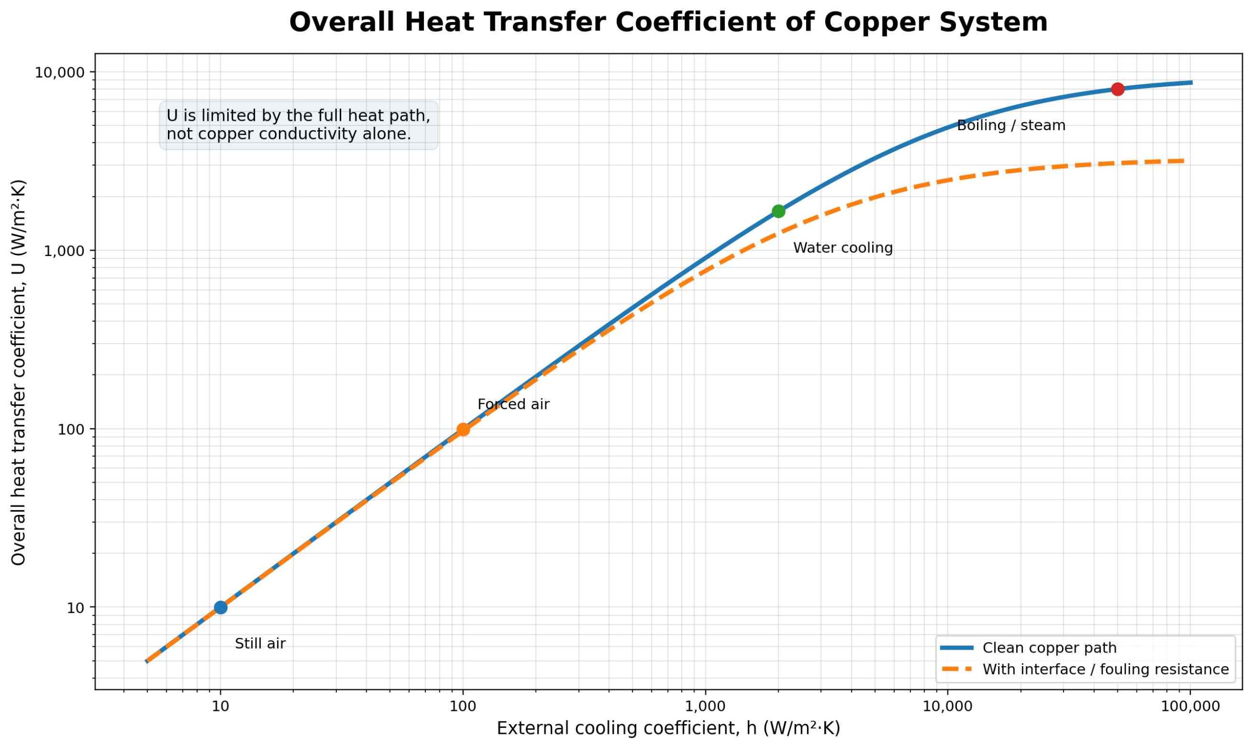
What Is the Overall Heat Transfer Coefficient of Copper?
The overall heat transfer coefficient, usually written as U, describes total heat transfer through a complete system. It includes all thermal resistance in the heat path.
This is different from the convective heat transfer coefficient h, which usually describes heat exchange at one surface.
For example, a copper tube heat exchanger may include:
- Heat transfer from hot fluid to the inner copper wall
- Heat conduction through the copper tube wall
- Heat transfer from the outer copper surface to air or water
- Fouling, oxidation, or coating resistance
- Contact resistance at joints or interfaces
The U-value combines these effects. This makes it useful for heat exchangers, cold plates, copper tubes, liquid cooling systems, and multilayer thermal structures.
The same concept applies to PCB thermal design.
A copper core PCB thermal path may include:
| Thermal Path Segment | Possible Thermal Issue |
|---|---|
| Component junction to package | Package thermal resistance |
| Package to solder joint | Solder voids or poor wetting |
| Solder joint to copper pad | Pad size and copper connection |
| Copper pad to copper plane/core | Copper thickness and layout |
| Copper layer to dielectric | Dielectric thermal conductivity |
| Board to heat sink or housing | Contact resistance and flatness |
| Housing to air | Airflow and surface area |
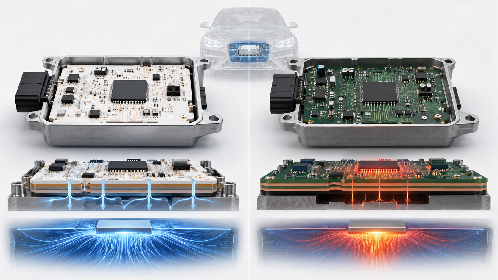
This is why real thermal performance cannot be judged by copper alone. Copper is important, but the complete heat path decides the final temperature.
Why Does the Heat Transfer Coefficient of Copper Matter in PCB, PCBA, and Heat Sink Design?
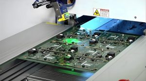
Copper is central to PCB manufacturing because it supports both electrical conduction and heat spreading. In high-power products, copper is not only a circuit material. It becomes part of the thermal management structure.
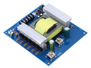
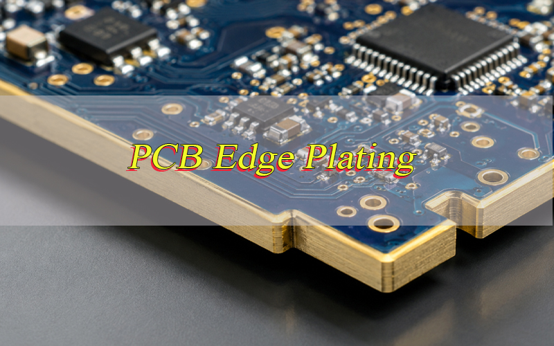
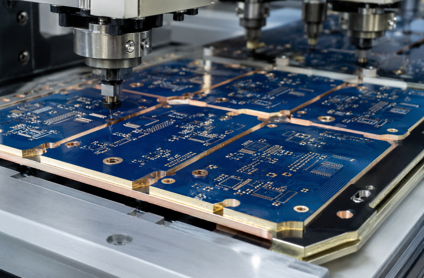
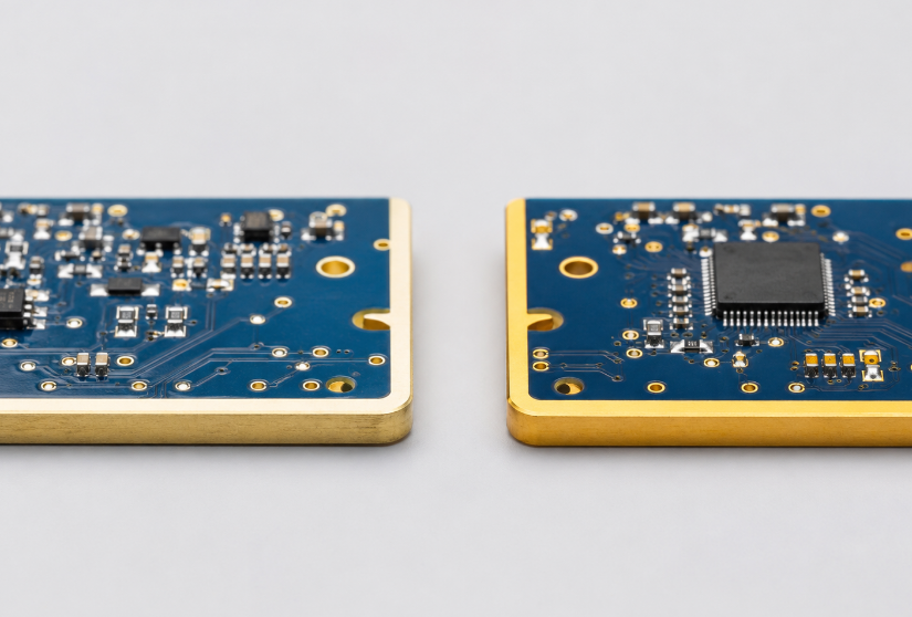
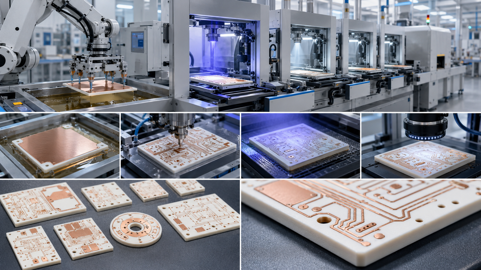
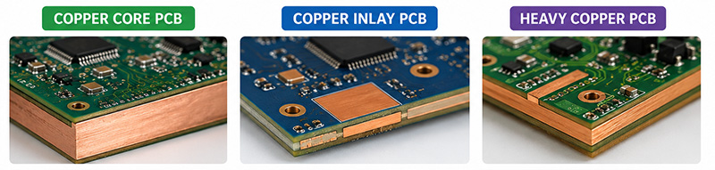
Heavy Copper PCB
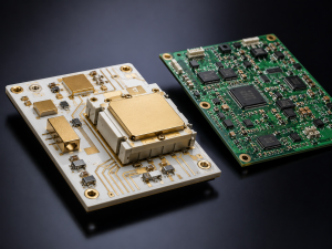
- Heavy copper PCB uses thicker copper to carry higher current and reduce resistance-related heating. It is often used in power supplies, EV chargers, battery systems, industrial controllers, motor drives, and automotive electronics.
- Heavy copper also helps spread heat from power components. However, thicker copper does not automatically solve every thermal problem. Designers must also check trace width, copper balance, etching tolerance, soldering quality, thermal relief design, and the final heat exit path.
- A common mistake is adding thick copper without improving airflow, heat sink contact, or board-to-housing conduction. In that case, heat spreads across the board but may not leave the product efficiently.
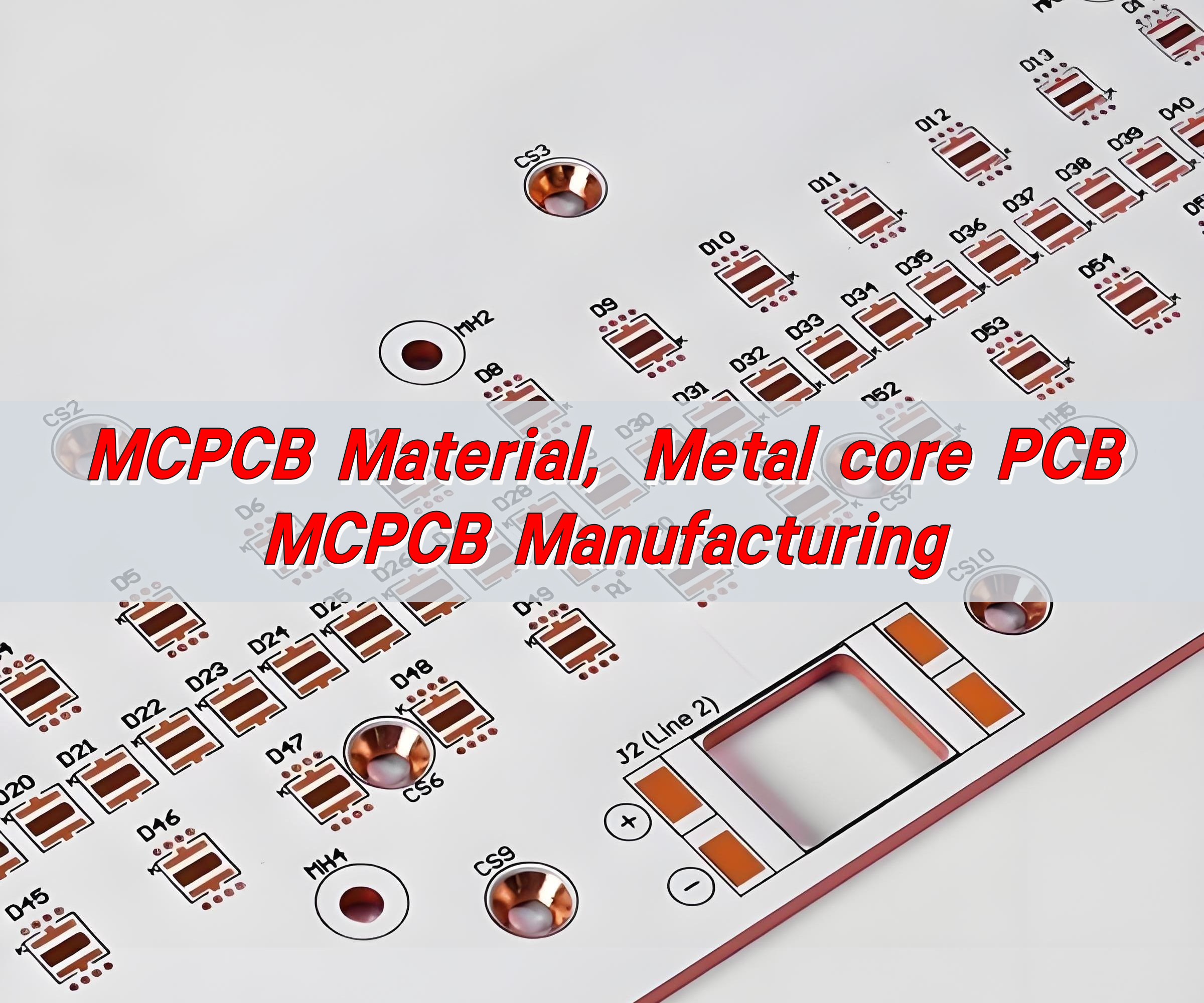
Copper Core PCB
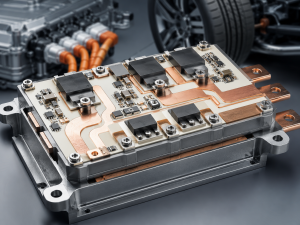
Copper core PCB uses a copper base or copper core to move heat away from components. Compared with standard FR4, copper core structures offer much stronger heat spreading.
Copper core PCB is useful for:
- High-power LED modules
- Automotive lighting
- MOSFET and IGBT boards
- EV charging systems
- Industrial power modules
- Compact power conversion boards
The copper core spreads heat quickly, while the final temperature depends on dielectric thermal conductivity, copper thickness, contact area, heat sink design, and airflow.
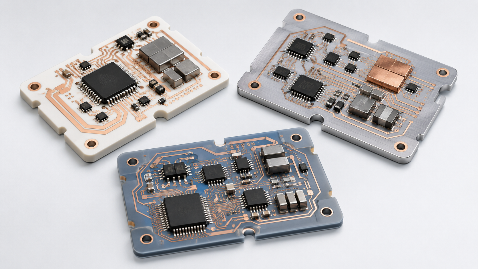
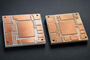
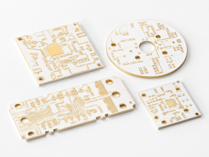
Copper Inlay and Copper Coin PCB
- Copper inlay and copper coin PCB structures place copper directly under high-heat components. This creates a shorter thermal path from the component to the heat dissipation structure.
- These designs are useful when heat is concentrated in a small area, such as under power ICs, RF devices, LEDs, high-current terminals, or power modules.
- For manufacturing, copper inlay and copper coin designs need careful DFM review. The supplier should check cavity tolerance, bonding reliability, copper thickness, lamination control, solderability, and board flatness.
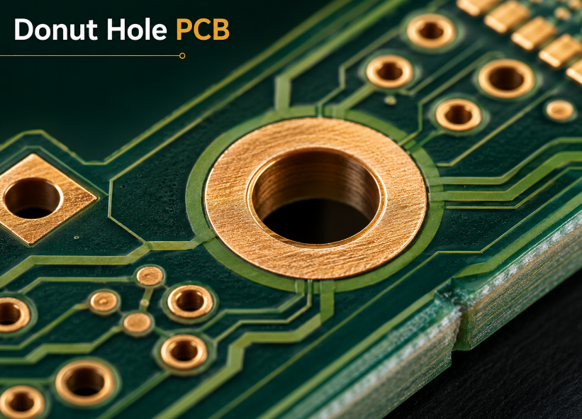
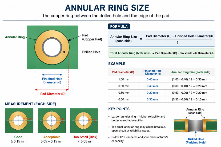
Thermal Vias and Copper Planes
Thermal vias transfer heat from one PCB layer to another. Copper planes spread heat across a wider area. Together, they help reduce hot spots.
For better performance:
- Place thermal vias close to the heat source
- Use enough via quantity and copper plating thickness
- Connect vias to large copper planes
- Avoid isolated copper areas with no heat exit path
- Consider solder wicking risk under components
- Check whether vias should be filled, capped, or tented
Thermal vias are useful, but they are not magic. If the bottom side has no heat sink, no airflow, or no metal housing contact, the improvement may be limited.
Heat Sink and Housing Contact
- A copper PCB or copper heat spreader needs a good contact path to the heat sink or enclosure. Poor contact pressure, uneven surfaces, air gaps, or weak thermal pads can reduce heat transfer.
- For high-power PCBA, mechanical assembly matters as much as PCB material. Screw positions, flatness, thermal grease, gap pad compression, and enclosure material should be reviewed during design.
Common Design Mistakes
Many thermal problems are caused by layout and structure decisions made before production. Common mistakes include:
| Mistake | Why It Causes Problems |
|---|---|
| Treating copper thermal conductivity as h value | Leads to wrong thermal assumptions |
| Adding copper without a heat exit path | Heat spreads but remains inside the product |
| Ignoring dielectric thermal resistance | Metal base performance becomes limited |
| Using too few thermal vias | Heat cannot move efficiently between layers |
| Placing thermal vias too far from the heat source | Thermal path becomes longer |
| Covering key copper areas with solder mask | Surface heat transfer and contact may be reduced |
| Poor heat sink contact | Contact resistance becomes the bottleneck |
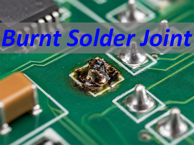
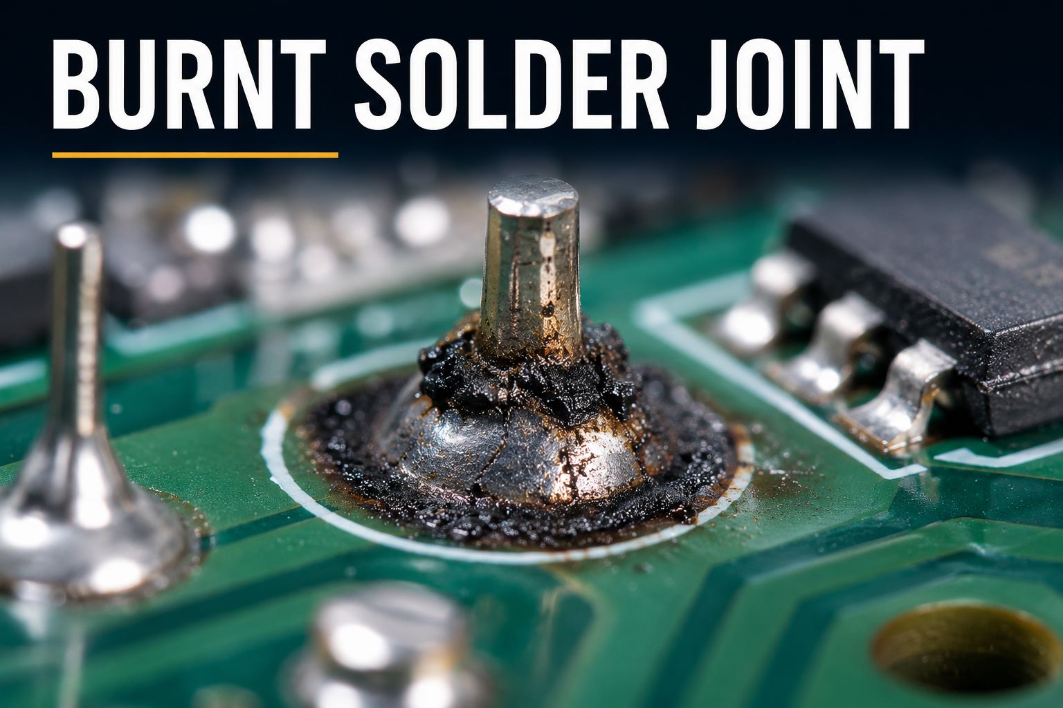
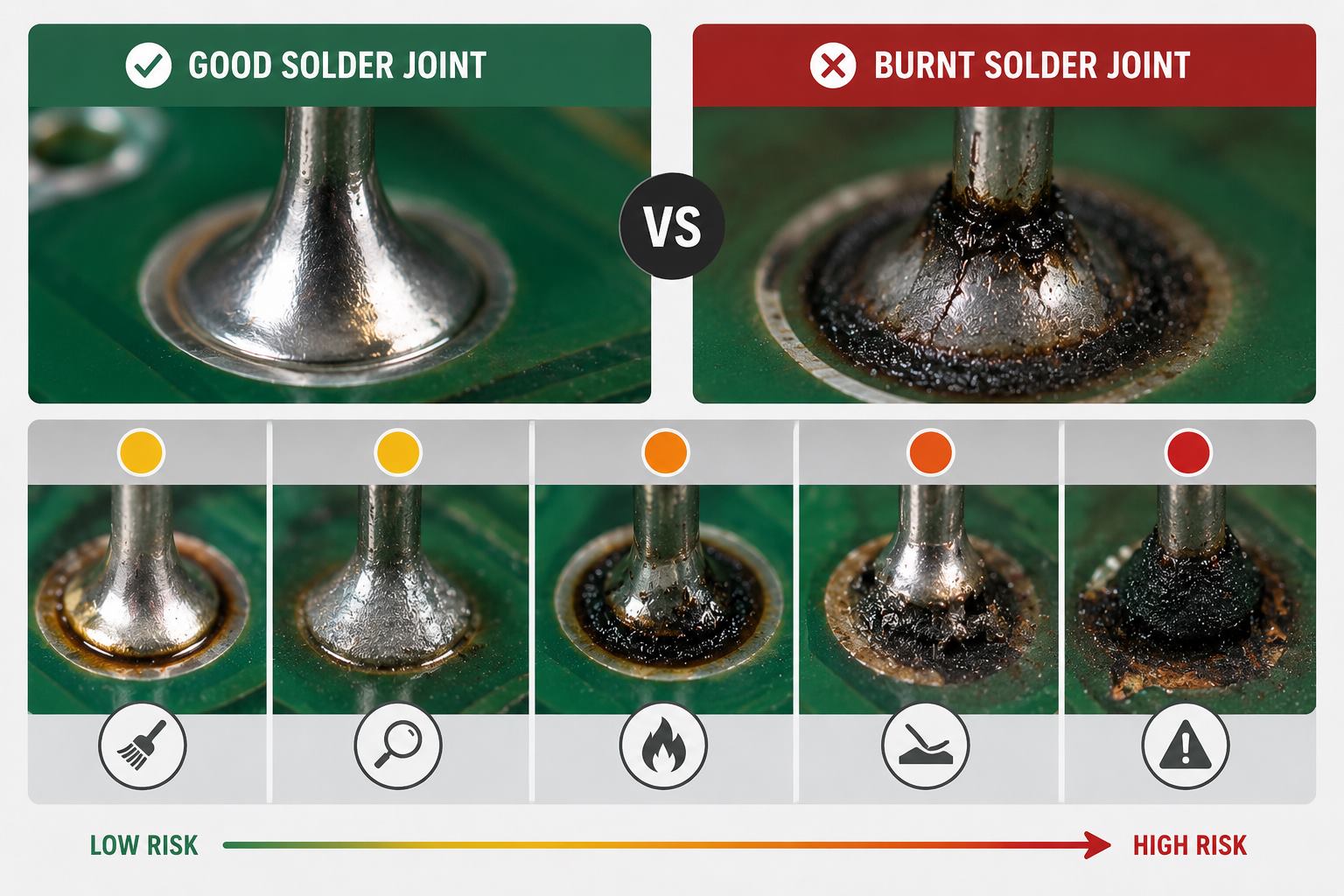
| Ignoring solder voids under power parts | Junction temperature may rise |
| Choosing heavy copper without DFM review | Etching, spacing, soldering, and warpage risks increase |
What Should Buyers Check Before Ordering Copper-Based Thermal PCBs?
For buyers and engineers, the right questions before ordering are important. A reliable PCB manufacturer should review not only board dimensions and copper thickness, but also the real thermal and electrical requirements.
Before ordering, check:
| Item to Check | Why It Matters |
|---|---|
| Copper thickness | Affects current capacity and heat spreading |
| Copper distribution | Affects warpage, etching, and thermal balance |
| Base material | FR4, aluminum, copper, or ceramic changes the thermal path |
| Dielectric thermal conductivity | Critical in metal core PCB |
| Thermal via design | Affects heat transfer between layers |
| Surface finish | Affects solderability, oxidation, and contact reliability |
| Solder mask opening | Affects exposed copper and heat sink contact |
| Heat sink contact area | Determines practical heat removal |
| Operating current | Affects Joule heating and trace temperature rise |
| Component power loss | Determines hot spot risk |
| Assembly method | Affects solder voids, contact, and reliability |
| Product environment | Airflow, enclosure, temperature, and humidity matter |
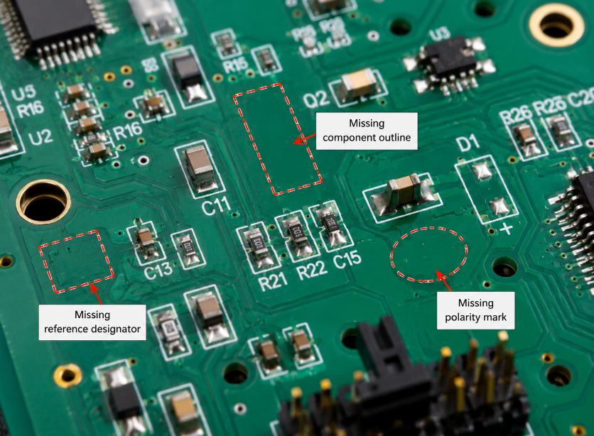
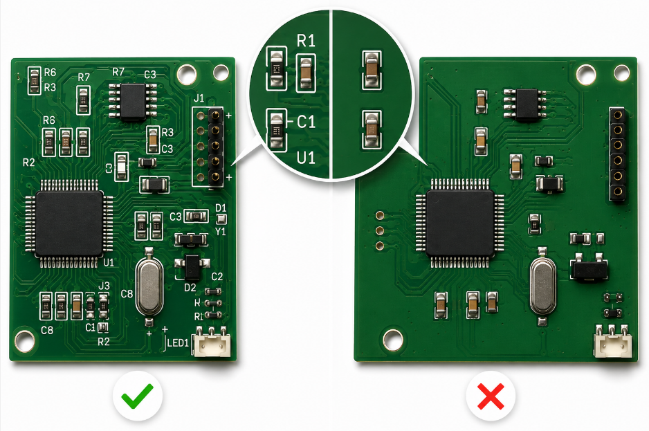
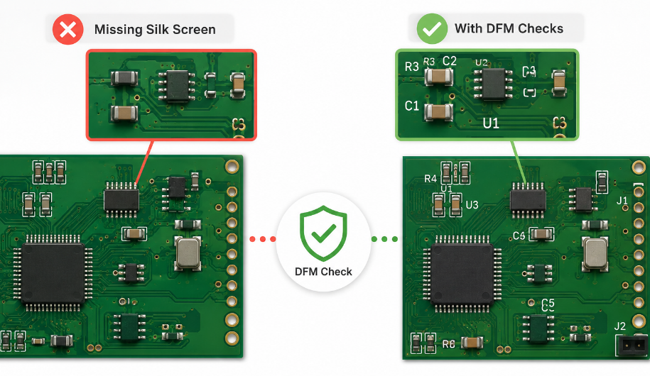
This is where PCB manufacturing experience becomes important. A design may look correct in a schematic, but production details can affect thermal performance. DFM review helps identify these risks before fabrication and assembly.
At Best Technology, thermal PCB projects are usually reviewed from several angles: copper structure, material selection, stack-up, thermal path, manufacturability, assembly reliability, and application environment.
FAQs About Heat Transfer Coefficient of Copper
Q1: What is the heat transfer coefficient of copper in W/m²·K?
There is no single universal value. Typical values may range from low natural air convection to very high liquid cooling or phase-change cooling values, depending on actual working conditions.
Q2: What is the heat transfer coefficient of copper to air?
Copper-to-air heat transfer is usually limited in still air. Forced airflow improves heat removal by reducing the warm boundary layer near the copper surface.
Q3: What is the heat transfer coefficient of copper and water?
Copper-to-water heat transfer is usually much stronger than copper-to-air heat transfer. This is why copper tubes, cold plates, and liquid cooling blocks are used in high-power systems.
Q4: Is copper better than aluminum for heat transfer?
Copper has higher thermal conductivity than aluminum, so it spreads heat faster. Aluminum is lighter and more cost-effective, so it is still widely used for heat sinks and LED aluminum PCBs.
Q5: Is copper better than stainless steel for thermal management?
Yes, when heat spreading is the main goal. Copper conducts heat much better than stainless steel. Stainless steel is usually chosen for strength, corrosion resistance, or structure.
Q6: What is the overall heat transfer coefficient of copper?
The overall heat transfer coefficient, or U-value, describes heat transfer through a complete system. It includes convection, conduction, surface condition, contact resistance, and other thermal barriers.
Q7: Why does the heat transfer coefficient of copper matter in PCB design?
It matters because copper spreads heat inside the PCB, but heat must still leave the board through air, heat sinks, metal housings, or liquid cooling. Good thermal PCB design must consider the complete heat path.
Q8: Can thicker copper always improve PCB heat dissipation?
Thicker copper can improve heat spreading and current capacity, but it does not always reduce final temperature. The board also needs a proper heat exit path, such as airflow, a heat sink, a metal base, or housing contact.
Q9: What PCB types are suitable for high thermal performance?
Common options include heavy copper PCB, copper core PCB, aluminum PCB, ceramic PCB, copper inlay PCB, and copper coin PCB. The best choice depends on power density, insulation requirement, current load, cost, and assembly structure.
To sum up, the heat transfer coefficient of copper is important in thermal design, but it should not be treated as a fixed copper material property. Copper has excellent thermal conductivity, which allows it to spread heat quickly. The heat transfer coefficient describes how efficiently heat leaves or enters the copper surface under specific cooling conditions.
For PCB and PCBA applications, copper plays a key role in heat spreading, current carrying, and product reliability. Heavy copper PCB, copper core PCB, copper inlay PCB, copper coin PCB, thermal vias, and copper planes can all improve thermal performance when they are designed with a complete heat path.
The best thermal design is not just about using more copper. It is about selecting the right copper structure, material stack-up, dielectric layer, surface finish, heat sink contact, airflow path, and assembly process.
At EBest Circuit (Best Technology), we support thermal management PCB and PCBA solutions, including copper core PCB, heavy copper PCB, aluminum PCB, ceramic PCB, copper inlay PCB, copper coin PCB, and full and partial turnkey PCB assembly. If your project involves LED modules, EV chargers, AI server power boards, industrial control boards, automotive PCBA, or high-current electronics, you can send your Gerber files, BOM, stack-up, copper thickness, and heat dissipation requirements to sales@bestpcbs.com for an engineering review and quotation.