PCB manufacturing PCB manufacturing
Home > Blog

IPC-TM-650 PCB Test Methods Guide: Cleanliness, Peel Strength and Thermal Stress

July 9th, 2026

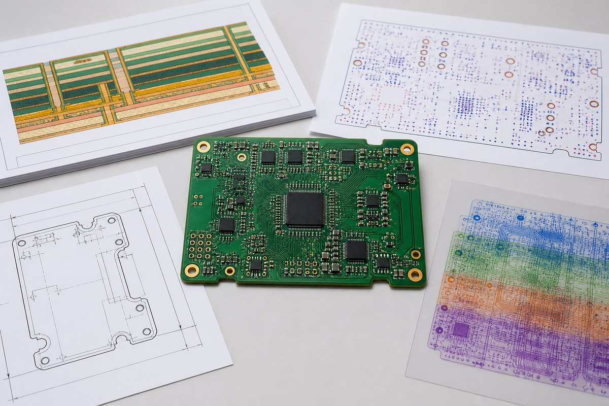
IPC-TM-650 gives PCB testing a clear and shared method. It explains how to prepare samples, run tests, measure results and record data for printed boards, PCB materials, copper foil, solder mask and assemblies.

For PCB projects, this matters because a board can look acceptable on the surface but still hide plating cracks, ionic residue, weak copper adhesion or poor thermal reliability. These problems may appear later during soldering, storage, rework or field use.

This guide focuses on cleanliness, microsectioning, peel strength, bow and twist, solder mask testing, thermal stress, thermal shock and test reports. It also explains how to read test results without confusing a test method with a final pass or fail decision.

IPC-TM-650, https://www.bestpcbs.com/blog/2026/07/ipc-tm-650-3/

What Is IPC-TM-650?

IPC-TM-650 is a test methods manual for PCB materials, printed boards, assemblies and related interconnection products. It defines sample preparation, test conditions, measurement methods and reporting format.

In PCB production, the manual is used to test internal structure, copper adhesion, ionic contamination, solder mask behavior, board flatness, solderability and thermal reliability. It is useful for multilayer PCB, HDI PCB, automotive PCB, medical PCB, aerospace PCB and other high-reliability projects.

It is not a simple quality checklist. It is a technical reference that makes PCB test results repeatable, comparable and easier to review across suppliers, labs and production batches.

What Is IPC-TM-650 Used for in PCB Testing?

IPC-TM-650 is used to check whether a PCB, material or process meets defined technical requirements. It supports process control, material qualification, supplier review, failure analysis and final quality inspection.

Common uses include:

  • PCB cleanliness review after fabrication or assembly.
  • Plated hole and via inspection through microsectioning.
  • Copper peel strength testing on laminate or finished boards.
  • Bow and twist measurement before SMT assembly.
  • Solder mask reliability testing under heat, chemicals or humidity.
  • Thermal stress testing for plated-through holes.
  • Solderability review for copper and finished surfaces.
  • Lot traceability support for bulk PCB and PCBA orders.

This makes the method set useful from prototype validation to mass production quality control.

What Are the Main IPC-TM-650 PCB Test Methods?

The main IPC-TM-650 PCB test methods cover reporting, visual, dimensional, chemical, mechanical, electrical and environmental testing. Each group targets a different quality risk.

CategoryCommon MethodPCB Use
Reporting1.4, 1.5Report format and result recording
Visual2.1.1Microsectioning and internal structure review
Dimensional2.4.22Bow, twist and PCB flatness
Chemical2.3.25Ionic contamination and ROSE testing
Mechanical2.4.8Peel strength of metallic clad laminates
Solderability2.4.12Edge dip solderability review
Solder Mask2.3.42, 2.4.28.1, 2.5.6.1, 2.6.3.1, 2.6.14Solvent resistance, adhesion, dielectric strength, moisture resistance and electrochemical migration
Environmental2.6.8, 2.6.7.2, 2.6.26Thermal stress, thermal shock, thermal cycling and interconnect reliability

For normal PCB production, the most practical areas are cleanliness, microsectioning, peel strength, bow and twist, solder mask testing and thermal stress. For HDI PCB, automotive PCB, medical PCB and aerospace PCB, extra reliability testing may be added because field failure cost is much higher.

What Does IPC-TM-650 2.1.1 Microsectioning Check?

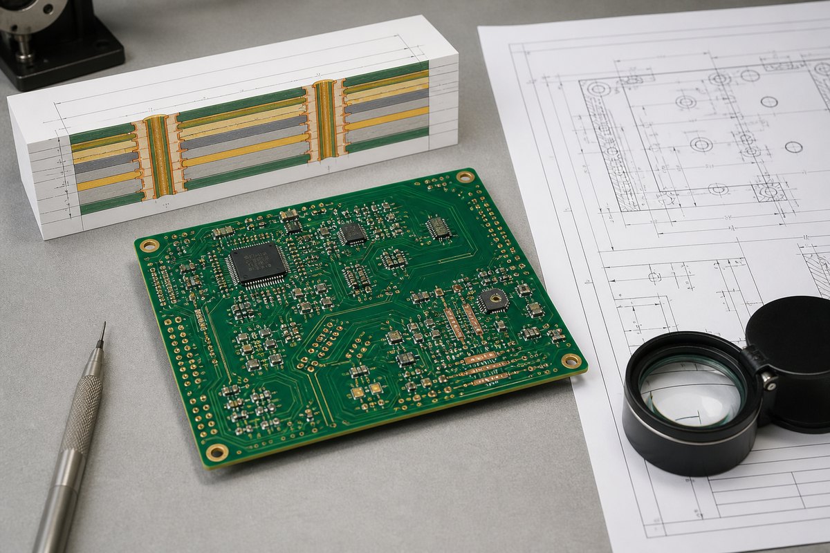
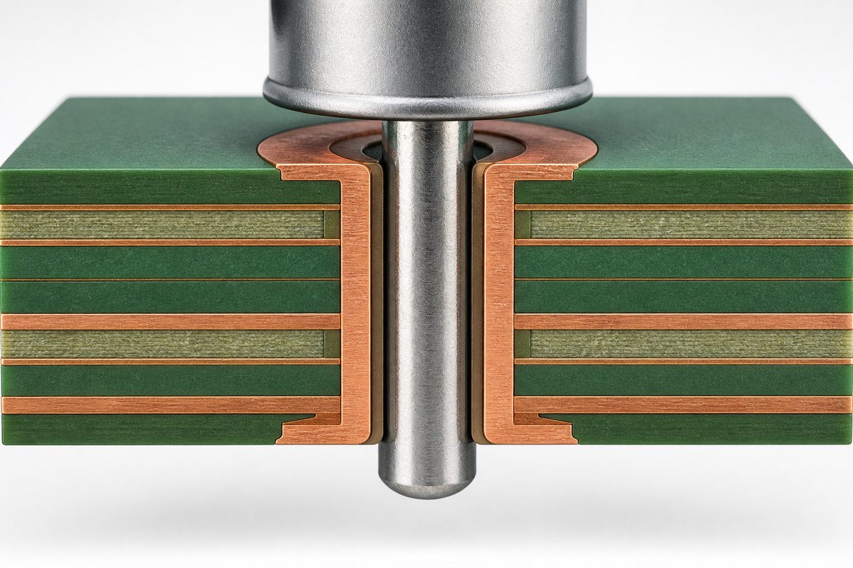
IPC-TM-650 2.1.1 microsectioning checks the internal structure of a PCB by cutting, mounting, grinding, polishing and inspecting a sample cross-section. It is destructive, but it shows defects that cannot be seen from the board surface.

This method can check:

  • Plated-through hole wall thickness
  • Via copper quality
  • Inner-layer connection
  • Copper plating uniformity
  • Laminate cracks
  • Resin recession
  • Void formation
  • Microvia structure
  • Solder joint cross-section
  • Delamination or separation

This section also works as a practical microsectioning guide for reading hidden PCB structure. It helps confirm whether drilling, desmear, plating, lamination and thermal processes are stable.

Which IPC-TM-650 Cleanliness Tests Are Used for PCBs?

Cleanliness testing checks whether harmful ionic or chemical residues remain on the PCB surface. These residues may come from plating chemistry, flux, cleaning, handling, soldering or environmental exposure.

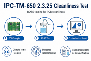
The most common method is IPC-TM-650 2.3.25 ROSE testing. ROSE means Resistivity of Solvent Extract. It extracts ionizable residues into a test solution and measures the contamination level.

Common cleanliness-related methods include:

  • IPC-TM-650 2.3.25: ROSE testing for ionizable residues.
  • Modified ROSE testing: used when a specific bare board process requires adjusted extraction control.
  • Ion chromatography: identifies specific ionic species.
  • SIR-related testing: checks insulation behavior under humidity and electrical bias.

ROSE testing is useful for process control, but it does not identify every contaminant. For high-reliability PCB, ion chromatography is often better for finding chloride, sulfate, bromide or weak organic acid residue.

IPC-TM-650 Cleanliness Test, https://www.bestpcbs.com/blog/2026/07/ipc-tm-650-3/

What Does IPC-TM-650 2.4.8 Peel Strength Testing Measure?

IPC-TM-650 2.4.8 peel strength testing measures the bonding strength between metallic cladding and the base laminate. In PCB production, it is mainly used to check copper foil adhesion.

Good peel strength helps prevent lifted pads, copper separation, trace peeling and delamination during soldering, rework, thermal cycling or mechanical handling. Poor peel strength may appear after chemical exposure, repeated heating or weak laminate bonding.

Peel strength can be affected by:

  • Copper foil type
  • Laminate resin system
  • Surface treatment
  • Copper thickness
  • Thermal history
  • Chemical process control
  • Test direction and sample condition

A useful test report should show the sample condition, copper weight, test direction, test speed and thermal exposure status.

What Does IPC-TM-650 2.4.22 Bow and Twist Testing Check?

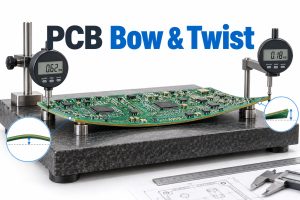
IPC-TM-650 2.4.22 bow and twist testing checks PCB flatness. Bow means the board bends smoothly in one direction. Twist means one or more corners move out of plane.

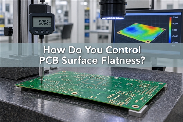
This test is important because a warped PCB can pass electrical testing but still create SMT assembly problems. Excessive bow or twist may cause uneven solder paste, component placement shift, BGA coplanarity issues, connector mismatch and solder joint stress.

Bow and twist risk is higher in:

  • Thin PCB
  • Large PCB panels
  • Unbalanced copper distribution
  • High-layer-count PCB
  • Heavy copper PCB
  • BGA designs
  • Fine-pitch SMT layouts
  • Rigid-flex PCB structures

Flatness should be checked before assembly, especially when the product uses dense components, press-fit connectors or large board sizes.

Which IPC-TM-650 Methods Are Used for Solder Mask Testing?

Solder mask testing checks whether the mask can protect copper, maintain insulation and survive production stress. Solder mask is not only a colored coating. It affects solder bridging, leakage risk, copper exposure and long-term PCB reliability.

Common solder mask test areas include:

  • Solvent resistance: checks whether cleaning agents damage the mask.
  • Adhesion: checks whether the mask peels, lifts or flakes.
  • Dielectric strength: checks insulation under voltage stress.
  • Moisture resistance: checks stability under humidity.
  • Thermal shock: checks cracking, blistering or separation.
  • Electrochemical migration resistance: checks leakage path risk under moisture and voltage.

For fine-pitch PCB, solder mask testing should be reviewed together with solder mask bridge width, expansion setting and registration capability. A good material can still fail in assembly if the opening design is too aggressive.

How Does IPC-TM-650 2.6.8 Test PCB Thermal Stress?

IPC-TM-650 2.6.8 thermal stress testing checks whether plated-through holes and related PCB structures can survive soldering heat. It is commonly used to evaluate plating reliability under short-term thermal exposure.

The test exposes the sample to a defined high-temperature solder or thermal condition. After exposure, the board may be inspected by microsectioning to check barrel cracks, corner cracks, inner-layer separation, plating defects or laminate damage.

This method is especially useful for:

  • Plated-through holes
  • Multilayer PCB
  • Thick PCB
  • High-Tg materials
  • Lead-free soldering conditions
  • Automotive PCB
  • Industrial control PCB
  • Aerospace and medical PCB

Thermal stress testing helps find plating weakness before boards enter assembly, rework or long-term service.

What Is the Difference Between IPC-TM-650 Thermal Stress and Thermal Shock?

IPC-TM-650 thermal stress and thermal shock both involve temperature, but they check different risks. Thermal stress focuses on soldering heat resistance. Thermal shock focuses on repeated fast temperature change.

ItemThermal StressThermal Shock
Typical Method2.6.8, 2.6.8.12.6.7, 2.6.7.2
Main PurposeChecks resistance to soldering or reflow heatChecks resistance to repeated hot and cold changes
Main RiskBarrel cracks, plating separation, laminate damageFatigue cracks, intermittent opens, material stress
Test StyleShort high-temperature exposureRepeated temperature cycling or shock
Common SamplePlated-through holes, laminates, couponsPrinted boards, coatings, interconnects
Best UseAssembly heat risk reviewLong-term reliability review
Follow-Up CheckMicrosection and visual reviewContinuity monitoring and failure analysis

Thermal stress is closer to manufacturing and soldering risk. Thermal shock is closer to lifetime reliability risk. A high-reliability PCB project may require both tests, especially when the board will face lead-free reflow, field temperature swing or repeated power cycling.

How Do You Choose the Right IPC-TM-650 Test Method?

Choose the right method based on the actual PCB risk, not by ordering every available test. A simple 2-layer PCB and a high-layer-count automotive PCB should not use the same test plan.

  • Check the product use first: consumer, industrial, medical, automotive and aerospace boards have different reliability levels.
  • Review the PCB structure: layer count, board thickness, via type, copper weight and HDI structure affect test selection.
  • Match the test to the failure risk: cleanliness uses ROSE, plating uses microsectioning, and flatness uses bow and twist testing.
  • Confirm the process concern: solderability, solder mask adhesion, thermal stress and moisture resistance target different production risks.
  • Define the acceptance source: use customer drawings, IPC-A-600, IPC-6012, procurement files or project specifications.
  • Set sample quantity and coupon location: test data should represent the production lot, not just a convenient sample.
  • Confirm the method revision: the test report should state the exact method number and revision.
  • Control test cost: choose tests that reduce real risk instead of adding low-value inspection items.

The right test plan should be clear enough for production, inspection and purchasing teams to understand before the order starts.

What Should an IPC-TM-650 Test Report Include?

A test report should show what was tested, how it was tested, what was measured and how the result was judged. A report that only says “Pass” is not enough for serious PCB quality review.

A complete report should include:

  • Test method number and revision: confirms the exact procedure used.
  • PCB part number and revision: connects the result to the correct design.
  • Production lot number: supports batch traceability.
  • Material type and stackup: shows the board construction under test.
  • Surface finish: affects solderability, storage and inspection results.
  • Sample quantity: shows how many pieces or coupons were tested.
  • Coupon location: explains where the test sample came from.
  • Test condition: includes temperature, time, solution, load or cycling condition.
  • Equipment status: confirms calibration or measurement control.
  • Measured result: gives real values instead of only pass or fail.
  • Photos or microsection images: support visual review when structure matters.
  • Acceptance criteria: shows which requirement was used for judgment.
  • Final conclusion: states whether the result meets the project requirement.
  • Traceability record: links the test to material batch, process record and shipment.

For global PCB supply, traceability is important. It connects the result to the production lot, material batch, process record and shipment, which reduces quality disputes after delivery.

What Are Common Mistakes When Reading IPC-TM-650 Results?

The most common mistake is reading test results as universal pass or fail answers. The method explains how testing is done, but acceptance depends on the PCB class, customer drawing, purchase file and reliability requirement.

Common mistakes include:

  • Ignoring the method revision: an old method may not match the current requirement.
  • Comparing different test conditions: time, temperature, solution and sample state can change the result.
  • Using ROSE results as full chemical analysis: ROSE does not identify every ion type.
  • Ignoring sample location: coupon data may not represent every dense area of the PCB.
  • Treating one sample as the full batch: sample size should match the risk and order requirement.
  • Confusing thermal stress with thermal conductivity: one checks reliability; the other describes heat transfer.
  • Reading bow and twist after poor storage: humidity, stacking and support can affect flatness.
  • Using uncontrolled IPC TM 650 PDF files: unofficial files may be outdated or incomplete.
  • Missing acceptance criteria: the test method alone does not always define the final decision.
  • Ignoring lot traceability: a result is weak if it cannot be linked to the real production batch.

A reliable result should connect the test method, measured data, sample condition, acceptance source and project requirement.

What Is the Difference Between IPC-TM-650, IPC-A-600 and IPC-6012?

IPC-TM-650, IPC-A-600 and IPC-6012 work together, but they do not do the same job. IPC-TM-650 defines how to test. IPC-A-600 shows bare PCB acceptability. IPC-6012 defines rigid PCB performance requirements.

DocumentMain RoleWhat It CoversBest Use
IPC-TM-650Test methods manualSample preparation, test conditions, measurement and reportingRunning PCB tests in a controlled way
IPC-A-600Acceptability guideTarget, acceptable and nonconforming bare PCB conditionsIncoming inspection and visual quality review
IPC-6012Performance specificationRigid PCB qualification, performance, final finish, holes, conductors and quality conformanceProcurement, qualification and production requirements

In practice, a rigid PCB may be purchased under IPC-6012, visually reviewed with IPC-A-600 and tested by methods from IPC-TM-650. The three documents should be used together when a project requires reliable quality control.

IPC-A-650 vs IPC-A-600 vs IPC-6012, https://www.bestpcbs.com/blog/2026/07/ipc-tm-650-3/

FAQs About IPC-TM-650

Q1: How do you know which revision to use for a test?

A1: Check the exact method number before testing. Different methods may have different revision dates, so there is no single “latest revision” for every test. A reliable report should show the method number, revision and test date. This prevents disputes when a customer, lab and PCB factory review the same result.

Q2: Can a PCB pass electrical test but still fail these methods?

A2: Yes. Electrical test mainly checks opens and shorts. It may not reveal ionic contamination, weak copper adhesion, barrel cracking, poor solder mask adhesion or board warpage. That is why microsectioning, cleanliness, peel strength, bow and twist and thermal stress testing are often used for higher-reliability PCB projects.

Q3: When is ROSE testing not enough for cleanliness review?

A3: ROSE testing is useful for fast process control, but it does not identify every contaminant. If the project involves high voltage, fine spacing, medical electronics, automotive electronics or corrosion risk, ion chromatography or SIR testing may be better. These tests provide more detailed residue or insulation reliability information.

Q4: Why does sample location matter in microsectioning?

A4: Microsectioning is destructive, so only selected coupons or board areas are inspected. If the sample comes from a low-risk area, it may miss defects near dense vias, heavy copper, BGA zones or high-current sections. For critical boards, sample location should reflect the most difficult structure on the PCB.

Q5: What can cause poor peel strength on a PCB?

A5: Poor peel strength may come from weak laminate bonding, copper foil treatment problems, poor surface preparation, excessive chemical attack, repeated heat exposure or unsuitable material selection. The risk is higher when the PCB faces lead-free reflow, rework, high temperature or mechanical stress during assembly and service.

Q6: Why is bow and twist important before SMT assembly?

A6: A warped board can cause solder paste thickness variation, placement offset, BGA coplanarity issues and connector fit problems. Even if the circuit passes electrical test, poor flatness can reduce SMT yield. Bow and twist review is especially important for thin, large, dense or high-layer-count PCB designs.

Q7: What should buyers avoid when searching for IPC TM 650 PDF files?

A7: Avoid using random IPC TM 650 free download files for purchasing or audit decisions. They may be outdated, incomplete or uncontrolled. For serious projects, confirm the controlled document source, method number and current revision for that specific test before writing requirements into a purchase order or quality agreement.

Q8: Which tests are useful for lead-free PCB assembly?

A8: Lead-free assembly usually brings higher reflow temperature, so thermal stress, solderability, solder mask reliability and microsectioning become more important. These tests help check plated-through hole reliability, surface wetting, solder mask stability and laminate resistance to heat before the PCB enters mass assembly.

Q9: What is the risk of using only a “Pass” statement in a report?

A9: A “Pass” statement alone does not show the method, sample size, test condition, measured value or acceptance source. This makes the report weak during customer review or failure analysis. A useful report should include real measured data, method revision, sample condition and acceptance criteria.

Q10: Do all PCB orders require the same test package?

A10: No. A simple prototype may only need standard inspection and electrical test. A high-reliability PCB may require cleanliness, microsectioning, thermal stress, solderability, SIR, CAF or thermal cycling review. The test package should match product risk, operating environment, reliability class and customer requirement.

Q11: Can these methods help with failure analysis?

A11: Yes. These methods can help locate the cause of field or assembly failure. Microsectioning can reveal cracks or plating defects. Cleanliness testing can show residue risk. Thermal stress can expose weak plated holes. Peel strength testing can show copper bonding problems. Together, they support root cause analysis and corrective action.

Q12: What should be included in a PCB purchase specification?

A12: A clear purchase specification should include PCB class, material, stackup, copper thickness, surface finish, acceptance standard, test method, sample quantity, report format and traceability requirement. For critical products, it should also define cleanliness limits, microsection requirements and thermal reliability expectations.

Q13: Why do high-reliability industries request more testing?

A13: Automotive, medical, aerospace and industrial control products often face longer service life, higher thermal stress, stricter safety requirements and higher failure cost. Extra testing helps reduce hidden defects before shipment. The focus is usually plating reliability, residue control, solderability, insulation resistance and long-term thermal performance.

Q14: Can EBest Circuit provide PCB and PCBA testing support?

A14: Yes. EBest Circuit can support PCB fabrication, PCBA assembly, custom production, batch orders and test report coordination based on project needs. For critical projects, the team can help review test method selection, sample requirements, manufacturing risk and report details before production starts.

Conclusion

IPC-TM-650 is valuable because it turns PCB testing into a controlled process. It helps define how samples are prepared, how tests are performed, what data should be measured and how results should be reported. For real production, the most useful areas are cleanliness control, microsectioning, peel strength, bow and twist, solder mask reliability and thermal stress testing.

For PCB selection, match the test plan to the board material, stackup, copper weight, via structure, surface finish, assembly process and operating environment. For procurement, do not accept vague reports. Ask for method numbers, revisions, measured values, sample details, acceptance criteria and lot traceability.

EBest Circuit is a China source PCB and PCBA manufacturer supporting prototype, custom PCB, batch PCB fabrication, PCBA assembly and global delivery. If you need reliable PCB manufacturing, PCBA service, test report support or a project quotation, contact us at sales@bestpcbs.com.

You may also like

IPC-2223 Standard for Flex PCB Design and Bend Radius

June 3rd, 2026

Is IPC-2223 affecting flex PCB bend reliability, production approval, and long-term product performance? Flexible and rigid-flex boards are widely used in compact electronic products, but small design errors can cause cracking, delamination, conductor fatigue, and costly project delays.

For this reason, IPC-2223 provides a structured reference for flex PCB design, bend radius control, material selection, and production documentation. When applied correctly, IPC 2223 helps improve reliability, reduce redesign, and support smoother project communication from quotation to delivery.

IPC-2223, https://www.bestpcbs.com/blog/2026/06/ipc-2223/

What is IPC 2223?

IPC 2223 is a sectional design standard for flexible and rigid-flexible printed boards. It works together with IPC-2221, which provides the general printed board design foundation, while IPC 2223 focuses on the special design requirements of flexible circuit structures.

Unlike rigid PCB guidance, this standard pays close attention to bend areas, flexible dielectric materials, conductor routing, coverlay openings, stiffeners, and rigid-to-flex transition zones. These details directly affect whether a flex PCB can survive assembly, installation, and long-term use.

In actual flex PCB projects, IPC 2223 works as a shared technical reference between the project side and the PCB manufacturer. It helps clarify stack-up, bend zones, hole placement, material structure, and reliability expectations before production starts.

What is the Latest Version of IPC-2223?

The current English version is IPC-2223E, released in January 2020. This revision is widely used for flexible and rigid-flex printed board design, especially where bend radius, manufacturing drawings, hole spacing, and flex-area conductor layout must be reviewed carefully.

Older versions such as IPC-2223A and IPC-2223D may still appear in legacy drawings, archived specifications, or old project documents. However, for new flex PCB projects, the active revision should be confirmed before quotation, design review, and production release.

A clear drawing note should state the applicable revision, such as IPC-2223E, together with other related standards. This avoids confusion when different teams refer to old internal files, outdated PDF copies, or supplier-side default requirements.

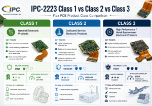
What is Difference between IPC 2223 Class 1, Class 2, Class 3?

IPC 2223 Class 1, Class 2, and Class 3 define different reliability levels for flexible and rigid-flex PCB projects. The higher the class, the stricter the requirement for material control, manufacturing consistency, inspection, and long-term product performance.

ClassProduct PositioningReliability LevelTypical ApplicationsDesign FocusQuality Control Focus
Class 1General electronic productsBasic reliabilityToys, simple consumer products, low-cost electronic modulesBasic electrical function, simple flex structure, cost-sensitive layoutVisual quality, basic continuity, general dimensional control
Class 2Commercial and industrial productsStable reliabilityIndustrial controls, communication devices, automotive accessories, medical support devicesBalanced bend radius, controlled stack-up, stable conductor routing, clear drawing notesElectrical test, material consistency, plating quality, bend area inspection
Class 3High-reliability productsHighest reliabilityAerospace electronics, critical medical devices, military electronics, high-end industrial systemsConservative bend radius, strict material selection, reinforced transition zones, optimized copper routingTight inspection, full documentation, strict acceptance criteria, higher process traceability
Cost LevelLowestMediumHighestCost rises with tighter requirementsMore testing and review increase total project cost
Production RiskLower requirement but less design marginModerate risk if data is clearHigher control requirement but better long-term reliabilityClass choice affects manufacturabilityClear class definition prevents later disputes
Best FitShort-life or simple-use productsMost commercial flex PCB projectsProducts where failure may cause serious lossMatch class to product useAvoid over-specifying or under-specifying

Class selection should match the actual use environment, expected service life, and risk level. For many flexible PCB projects, Class 2 offers a practical balance between cost, reliability, and production control, while Class 3 is more suitable for critical applications with strict reliability targets.

IPC-2221 Class 1 vs Class 2 vs Class 3, https://www.bestpcbs.com/blog/2026/06/ipc-2223/

What Does IPC-2223 Cover in Flex PCB Design?

IPC-2223 covers the design details that make flexible and rigid-flex boards manufacturable, bendable, and reliable. Its scope includes flex board types, material structures, component mounting forms, interconnection design, and mechanical reliability control.

The standard addresses single-sided, double-sided, multilayer, and rigid-flex constructions. It also considers adhesive and adhesiveless materials, insulating films, metallic conductors, reinforced or non-reinforced dielectric layers, and different flex circuit structures.

In real projects, IPC 2223 is useful for reviewing bend regions, conductor width, spacing, coverlay access, stiffener placement, via location, and transition areas between rigid and flexible sections. These design points directly affect yield, assembly stability, and field reliability.

Why is IPC-2223 Important for Flexible PCB Reliability?

IPC-2223 is important because flexible PCBs fail in different ways from rigid boards. A rigid PCB mainly faces thermal, electrical, and assembly stress, while a flex PCB also faces bending, folding, vibration, and mechanical movement.

If a bend area is designed with sharp corners, poor copper routing, unsuitable material thickness, or vias placed too close to the flex zone, the board can crack during installation or operation. Therefore, bend reliability must be treated as a core design target, not a final inspection item.

IPC 2223 helps reduce these risks by guiding how materials, conductor paths, and mechanical structures should be arranged. As a result, the project can gain better production yield, fewer quality disputes, and more stable performance after assembly.

What Materials and Structures Are Defined in IPC-2223 Flex PCB Design?

IPC-2223 defines flex PCB structures around insulating films, dielectric layers, adhesives, metallic conductors, coverlay, and stiffeners. These materials work together to provide both electrical connection and mechanical flexibility.

Common flex circuit materials include polyimide films, copper foil, adhesive systems, adhesiveless laminate, and protective coverlay. For rigid-flex boards, the structure also includes rigid laminate sections, plated through holes, and transition areas between rigid and flexible zones.

The material decision affects bend radius, thickness, heat resistance, dimensional stability, and cost. For example, thinner flexible layers usually support better bending performance, while added stiffeners can improve component mounting strength in selected areas.

IPC-2223 Specification for Flex PCB Design and Bend Radius

IPC-2223 specification focuses on the structure, bendability, material control, and reliability of flexible and rigid-flex printed boards. The following table summarizes key design areas that should be reviewed before production.

Specification AreaKey RequirementDesign PurposeProject Review Point
Flex MaterialPolyimide, copper foil, adhesive or adhesiveless laminateSupport flexibility, heat resistance, and dimensional stabilityConfirm material type, thickness, copper weight, and Tg requirement
Bend RadiusRadius must match total flex thickness and bend typeReduce copper fatigue, cracking, and delaminationDefine static bend or dynamic bend clearly on the drawing
Copper RoutingTraces should avoid sharp corners in bend areasImprove stress distribution during bendingUse smooth routing and avoid sudden width changes
Via PlacementVias should not be placed in active bend zonesPrevent barrel cracking and open circuitsKeep vias away from repeated bending areas
Coverlay DesignOpenings must match pads and access areasProtect conductors while keeping solderable areas exposedCheck coverlay registration and opening clearance
Stiffener AreaStiffeners should support connectors or mounted partsImprove mechanical strength where flexibility is not requiredDefine stiffener material, thickness, and location
Rigid-Flex TransitionTransition zones must avoid stress concentrationProtect copper and dielectric layers from crackingKeep copper routing smooth near rigid-to-flex boundaries
Layer Stack-UpLayer count and thickness must support the bend requirementBalance circuit density and flexibilityAvoid excessive thickness in tight bend areas
Hole-to-Edge SpacingHoles require safe spacing from board edge and bend zonesReduce cracking and production defectsReview drilled holes, slots, and edge clearance
Drawing NotesIPC class, material, bend radius, and surface finish should be definedReduce communication errors before productionAdd clear notes for class level and special flex requirements

This section is most valuable when used before quotation and production release. Clear IPC-2223 design data helps reduce redesign, sample failure, delivery delay, and quality disagreement.

IPC-2223 Bend Radius, https://www.bestpcbs.com/blog/2026/06/ipc-2223/

How to Calculate Bend Radius for IPC-2223 Flex PCB?

Bend radius calculation should start from flex thickness, bend type, copper structure, and product movement conditions. A smaller product space does not automatically mean the flex circuit can accept a smaller radius.

Step 1: Confirm the total flex thickness.
Calculate the full flexible area thickness, including copper, dielectric film, adhesive, coverlay, and any additional protective layer. Thicker flex sections normally require a larger bend radius because the material stack is less flexible.

Step 2: Define the bending condition.
Confirm whether the flex PCB is bent once during installation or moves repeatedly during product operation. A static bend usually allows more design freedom, while dynamic bending requires more conservative structure and larger safety margin.

Step 3: Check copper layer count and copper weight.
More copper layers and heavier copper reduce flexibility. For tight bend areas, the structure should avoid unnecessary copper thickness, excessive layer count, and dense copper features that increase mechanical stress.

Step 4: Review the trace direction in the bend area.
Traces should pass through the bend area smoothly and should avoid sharp corners. Curved routing and gradual transitions help reduce stress concentration, especially in flexible circuits exposed to repeated movement.

Step 5: Keep vias, pads, and solder joints away from the bend zone.
These features are mechanically sensitive and may crack under bending stress. The bend area should remain as clean and simple as possible to improve long-term reliability.

Step 6: Match the bend radius with the manufacturing capability.
Before final release, the selected bend radius should be reviewed together with the PCB manufacturer. Material type, stack-up, production tolerance, and final assembly shape all affect whether the design is practical.

Step 7: Mark the bend radius clearly on the drawing.
The drawing should show bend direction, bend area, bend radius, stiffener location, and whether the bend is static or dynamic. Clear documentation helps prevent misinterpretation before sample production.

What Are Common Design Mistakes in IPC-2223 Flex PCB Projects?

Common IPC-2223 flex PCB mistakes usually come from ignoring mechanical stress in bend areas. Flexible circuits are not simply thin rigid boards, so the layout must consider bending, folding, installation pressure, and repeated movement.

  • Placing vias inside the bend area
    Vias are weak points under repeated bending. Placing them in active flex zones may cause barrel cracks, open circuits, or unstable electrical performance.
  • Using sharp trace corners in flexible regions
    Sharp corners concentrate stress and increase the risk of copper fatigue. Smooth curves and gradual direction changes are better for bend reliability.
  • Choosing an overly thick stack-up
    Too many layers, heavy copper, or thick dielectric materials make the flex area harder to bend. This can cause delamination, cracking, or poor installation fit.
  • Ignoring rigid-to-flex transition stress
    The transition between rigid and flexible sections is a high-risk area. Poor copper routing or stiffener placement near this zone may create early failure.
  • Placing components too close to bend zones
    Components, pads, and solder joints should stay away from flexible bending areas. Mechanical movement can damage solder joints or lift pads over time.
  • Leaving bend radius unclear on drawings
    If the bend radius, bend direction, or bend type is not marked clearly, production review becomes unreliable. Ambiguous drawings often lead to sample delays or redesign.
  • Using unsuitable stiffener design
    Stiffeners improve local strength, but poor placement can create stress at the edge. The stiffener boundary should be reviewed carefully in relation to the bend area.
  • Only checking electrical function
    A flex PCB may pass electrical testing but still fail after bending. Mechanical reliability must be reviewed together with electrical performance.

How Does IPC-2223 Differ from IPC-2221 and IPC-6013?

IPC-2223, IPC-2221, and IPC-6013 are related PCB standards, but they are used for different purposes in a flex PCB project. IPC-2221 gives the general design foundation, IPC-2223 focuses on flexible and rigid-flex PCB design, while IPC-6013 is mainly used for performance and qualification control.
StandardMain FunctionScopeFlex PCB FocusUse StagePractical Value
IPC-2221General PCB design standardCovers common printed board design principles for different PCB typesProvides basic design guidance, but does not deeply address bend radius, flex stack-up, or dynamic bendingEarly design planningHelps build a general design framework before applying flex-specific rules
IPC-2223Flexible and rigid-flex PCB design standardCovers flex PCB structures, bend areas, coverlay, stiffeners, conductor routing, and rigid-flex transitionsDirectly focuses on flex PCB design, bend radius control, material structure, and mechanical reliabilityFlex PCB layout, stack-up review, and design releaseHelps reduce cracking, copper fatigue, delamination, and bend-area failure
IPC-6013Flexible printed board performance standardCovers qualification, acceptance, testing, and performance requirements for finished flexible boardsFocuses on whether the completed flex PCB meets quality and reliability requirementsProduction inspection and final acceptanceHelps confirm finished board quality through measurable acceptance criteria

In simple terms, IPC-2221 is the general design base, IPC-2223 is the flex PCB design guide, and IPC-6013 is the finished board performance reference. They should not be treated as interchangeable standards.

For a reliable flex PCB project, IPC-2223 is especially important during design review. IPC-6013 becomes more important after production, when the finished board must be checked against performance and acceptance requirements.

IPC-2223 vs IPC-2221 vs IPC-6013, https://www.bestpcbs.com/blog/2026/06/ipc-2223/

Where Can I Download IPC 2223 PDF?

IPC 2223 PDF should be obtained from official or authorized IPC channels. Since IPC standards are copyrighted documents, downloading free unofficial PDF copies can create version risk, compliance problems, and inaccurate technical references.

The safest method is to purchase or access the standard through the IPC store or authorized standards platforms. This helps ensure that the project uses the correct revision, correct language, and complete technical content.

For quotation or production review, sharing clear project requirements is usually better than sending an unclear downloaded file. A clear drawing note such as “Design reference: IPC-2223E” can help the PCB manufacturer understand the expected design basis. Attached is IPC 2223 PDF for your reference:

FAQs About IPC-2223 Standard

Q1: Is IPC-2223 only for flexible PCB projects?
A1: IPC-2223 is mainly used for flexible and rigid-flexible printed board design. It is especially valuable when the board includes bend areas, flexible material layers, coverlay, stiffeners, or rigid-to-flex transition zones.

Q2: Can IPC-2223 help reduce flex PCB cracking?
A2: Yes. IPC 2223 can help reduce cracking risk by guiding bend radius, conductor routing, material structure, and transition design. However, final reliability also depends on material choice, manufacturing control, assembly handling, and actual use conditions.

Q3: Is IPC-2223 enough for final product acceptance?
A3: IPC-2223 is a design standard, so it should not be used alone for final acceptance. For performance and qualification, projects often reference IPC-6013 together with the design requirements.

Q4: Should every flex PCB project use the same bend radius?
A4: No. Bend radius depends on flex thickness, copper weight, layer count, bend type, and movement frequency. A static bend can usually accept a different design margin than a dynamic flexing application.

Q5: Why do old drawings still mention IPC-2223A or IPC-2223D?
A5: Many legacy projects continue using old revision notes because the original product was approved years ago. For new projects, the revision should be reviewed and updated before design release or production transfer.

Q6: Does IPC-2223 apply to rigid-flex PCB stack-up review?
A6: Yes. IPC-2223 is highly relevant to rigid-flex stack-up review, especially where flexible layers pass through rigid sections, bend regions, plated holes, and transition areas.

Q7: What information should be confirmed before requesting a flex PCB quote?
A7: A quote request should include board type, layer count, material preference, copper thickness, bend radius, stiffener details, surface finish, class level, drawing notes, and expected annual quantity.

Get a Reliable Flex PCB Quote Based on IPC-2223 Requirements

A successful flex PCB project starts with clear design rules, reliable manufacturing control, and fast technical alignment. If your project involves bend radius limits, rigid-flex stack-up, tight assembly space, or high-reliability use, choosing a capable PCB partner can reduce risk before production begins.

EBest provides customized flex PCB and rigid-flex PCB manufacturing support with professional review, stable quality control, and responsive project communication. Send your Gerber files, drawings, stack-up, and IPC-2223 requirements to sales@bestpcbs.com to get a practical solution and fast quotation for your next flex PCB project.
You may also like