PCB to PCB soldering joins compatible conductive features on two circuit boards into a permanent electrical connection. A castellated module can sit directly on matching carrier-board pads, while soldered pins can connect boards at a defined spacing. Reliability starts with the joint geometry, access for heating and inspection, and a mechanical support arrangement that does not ask small solder joints to carry the entire assembly.
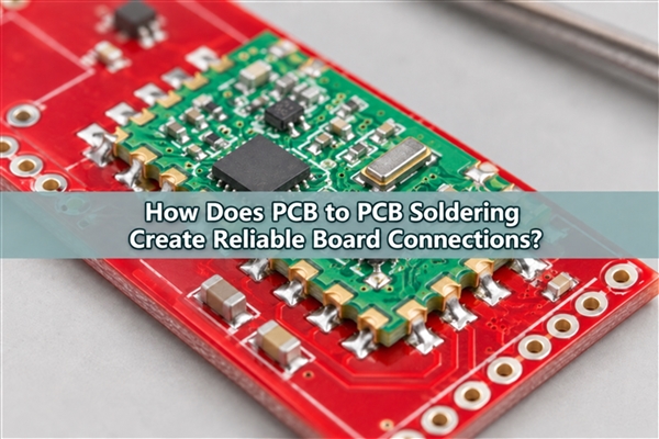
Can You Solder One PCB Directly to Another?
Yes, when both boards have solderable features intended to meet. Plated half-holes around a module edge are a common example: each half-hole aligns with a carrier land, and solder connects the exposed plating to that land. Two arbitrary board edges covered in solder mask will not form the same connection.
Decide whether the connection needs to be permanent before choosing the layout. A soldered module can reduce connector height and part count, but replacing it requires controlled rework. A separable board-to-board connector is generally more practical where routine servicing or repeated removal is part of the product requirement. Direct soldering also leaves less freedom to accommodate footprint errors after fabrication.
Which Connections Are Suitable for PCB to PCB Soldering?
The relevant types of PCB soldering depend on how the two boards meet. Start with board orientation, service access and mechanical loads, then select the joining process. A continuous solder bead along unrelated board edges is not a substitute for a designed interconnect.
| Connection | Suitable arrangement | What the design must provide |
|---|---|---|
| Castellated module | Small module mounted flat on a carrier | Matched lands, controlled placement, solder access and required underside clearances |
| Soldered pins or headers | Boards separated vertically or joined at an angle | Compatible holes and pins, spacing control, access to each soldered end and support |
| Designed edge or tab joint | Fixed board geometry with exposed joining lands | Defined copper geometry, a locating fixture and a validated load path |
| Flex termination soldered to a rigid board | Low-profile flexible interconnect | Purpose-designed exposed fingers, alignment support and strain relief outside the joint |
When soldering header pins to PCB holes on both boards, hold the boards at the specified spacing while the joints solidify. Confirm access to both ends before choosing this construction. Short wire links are another option when the board positions cannot be matched directly. They require strain relief and routing space, and they are not equivalent to a compact surface-mounted module. For high-speed signals or substantial current, evaluate the complete connection path rather than assuming that fewer parts automatically means better performance.
How Do Castellated Holes Connect a Module to a Carrier Board?
Castellated holes are plated holes intersected by the finished PCB edge. Their exposed, curved copper walls provide solderable surfaces beside the module. The carrier’s land extends into the matching connection region so solder can wet both surfaces. The visible outside fillet provides useful inspection access, although it cannot reveal every hidden interface beneath the module.
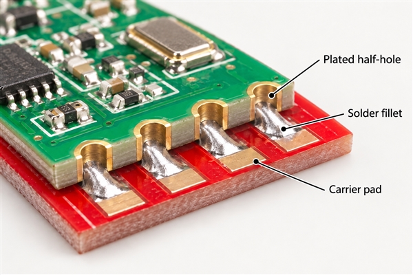
Half-hole plating quality, edge definition and land registration matter before assembly starts. A damaged or poorly plated edge cannot be corrected simply by adding more solder. For a new module design, specify the finished outline and half-hole requirements together with the carrier footprint; do not derive production dimensions from a photograph.
On FR4 PCBs, board thickness, copper distribution and surface finish also affect how the joint heats and wets. The module manufacturer’s recommended land pattern remains the starting point when using an existing module.
How Should the Two PCB Footprints Be Matched?
Compare both coordinate systems, not just the nominal pitch. Check pin 1, rotation, row spacing, board outline tolerance, pad dimensions and any module features extending underneath. A footprint that appears correct from above can still put copper beneath an antenna keepout or interfere with a bottom-side component.
- Use the current module drawing and its specified carrier land pattern.
- Check solder-mask openings and whether the module sits flat without unintended contact.
- Allow tool and inspection access around the perimeter.
- Review routing, copper balance and large ground connections that change local heat demand.
- Keep antenna, exposed-contact and mechanical keepouts consistent across both drawings.
- Provide fiducials or other suitable placement references for the assembly process.
Do a dry fit before soldering prototypes. If one end aligns but the other does not, stop and investigate dimensions or orientation. Pulling a board into place with solder can leave misregistration or residual stress that becomes visible only after cooling.
How Do You Hand-Solder Two PCBs Together?
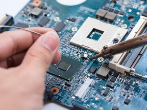
Hand soldering is useful for accessible castellated joints and prototypes. The essential PCB soldering techniques are controlled alignment, heating both mating surfaces and limiting solder volume. Use a stable holder, magnification, appropriate fume extraction and an ESD-controlled setup for sensitive assemblies. Disconnect all power and batteries.
- Inspect the lands and half-holes for damage or contamination. Use a cleaning method compatible with the board and components.
- Place the module in its intended orientation and apply compatible flux where needed.
- Tack one accessible corner with a small amount of solder, then verify the entire footprint before fixing the opposite side.
- Place the PCB soldering iron tip so it transfers heat to both the carrier land and the module’s plated edge.
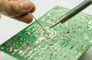
- Feed a controlled amount of solder to the heated joint. Withdraw the solder wire, then the tip, and let the joint solidify without movement.
- Complete the remaining connections, checking alignment and bridges as work progresses.
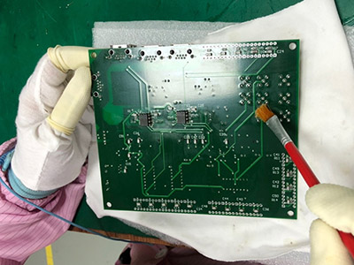
- Clean residues only as required by the flux chemistry and product process, then inspect and test.
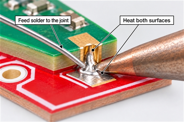
Choose solder wire for PCB soldering with an alloy, flux core and diameter appropriate to the joint. A large wire can make small deposits difficult to control. Do not use plumbing flux on electronic assemblies. If the tip cannot reach both surfaces, redesign the access or use a suitable assembly process instead of heating nearby components for an extended time.
A PCB soldering kit marketed for soldering circuit boards for beginners may supply an iron and wire without suitable magnification, holding support or a correctly sized tip. Check those requirements separately, and practice the same joint geometry on scrap or training boards before handling a valuable module.
When Should You Use Reflow Soldering for PCB Modules?
Reflow is appropriate when the module is qualified for that process and the carrier layout supports repeatable paste printing and placement. It can join many connections in one controlled cycle, including connections that are impractical to hand-solder. The module and every already-installed component must tolerate the planned thermal exposure.
Specify paste deposit requirements through the SMT stencil design rather than treating the stencil as a copy of the copper artwork. Aperture geometry and stencil thickness influence deposited volume, bridging and module seating. Inspect the print and placement before reflow; an oven cannot correct a misaligned footprint.
A PCB soldering machine setpoint alone does not establish a valid profile. Measure the loaded assembly and examine both the thermally heavy joints and heat-sensitive locations. Count earlier reflow operations on the module, not only the carrier’s latest pass. Follow the actual module’s limits for reflow exposure, moisture handling and orientation.
What Temperature Should You Use for PCB to PCB Soldering?
There is no single temperature that applies to every two-board assembly. For hand soldering, the iron setpoint is a tool setting; the joint temperature depends on tip contact, tip size, thermal recovery, copper area and heating time. A very fine tip may transfer heat poorly to a large ground connection even when its setpoint is high.
For reflow, use the solder paste’s recommended process window within the limits of the module, laminate and other components. Peak temperature, time above the alloy’s liquidus, ramp and cooling conditions all matter. Do not transfer a temperature from a different alloy or module into a production instruction without qualification.
When a joint heats slowly, first check contact area, tip condition, flux activity and the thermal load. Raising temperature repeatedly can damage pads or components without fixing the root cause. Where preheating is appropriate, control it as part of the complete process and verify the actual assembly temperature.
Can You Solder Flex PCB to Rigid PCB?
Soldering flex PCB to rigid PCB is possible when the flex has exposed termination features designed for the connection. The flexible dielectric itself is not solderable. Finger pitch, coverlay opening, surface finish and support near the termination must suit the selected hand, reflow or specialized joining process.
Keep the intended bend away from the soldered transition. Solder wicking into a flexible conductor can create a locally stiff region, concentrating strain at its end. A fixture or stiffened termination can maintain alignment during joining, while the product’s strain relief controls movement afterward. Do not repeatedly flex a finished joint to demonstrate that the cable is flexible.
A purpose-designed rigid-flex board can remove a separate soldered interface, but it changes the board construction and cost. A connector may be preferable when the flex must be replaced. Choose among these options before committing to a footprint, not after assembly problems appear.
How Can You Prevent Solder Bridges and Poor Wetting?
Inspect the geometry and process together. Excess solder, shifted placement, unsuitable paste deposits and closely spaced lands can create bridges. Oxidized or contaminated surfaces, exhausted flux and inadequate heat transfer can prevent wetting. Adding flux is not a reliable repair for missing plating or a lifted pad.
| Observation | First checks | Controlled response |
|---|---|---|
| Solder connects neighboring lands | Placement, deposit volume, land spacing | Remove the bridge using a qualified rework method, then inspect for damage and shorts. |
| Solder beads up instead of wetting | Surface condition, flux compatibility, actual heat transfer | Identify the cause before reheating; replace damaged material when necessary. |
| Module sits tilted | Underside interference, uneven deposits, first tack position | Correct seating through controlled rework; do not force the board flat after solidification. |
| Land or plating lifts | Thermal exposure and mechanical force | Stop rework and assess conductor integrity against an approved repair disposition. |
A matte joint is not automatically a cold joint, particularly with lead-free alloys. Evaluate wetting, connection geometry and evidence of disturbance against the specified acceptance criteria rather than demanding a uniformly shiny appearance.
How Should PCB-to-PCB Solder Joints Be Inspected?
Start with orientation and seating, then inspect every accessible joint for bridging, wetting, damage and contact with unintended conductors. Use magnification and lighting that reveal the module edge rather than hiding it behind reflections. Record the location of a suspect joint so rework and retest remain traceable.
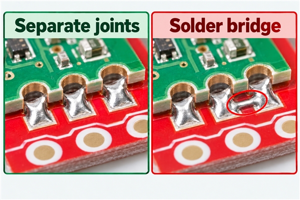
Follow visual inspection with the electrical tests appropriate to the circuit. Check for unintended supply shorts before first power-up, then use a controlled power-on procedure and the agreed functional test. Continuity alone cannot show that a mechanically weak joint will survive service, and a powered module that starts once has not passed environmental reliability testing.
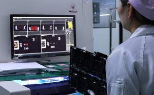
At EBest Circuit (Best Technology), our PCB assembly services include solder-paste inspection, AOI, X-ray inspection and functional testing. We use equipment including the SINIC-TEK S8080 3D SPI and UNICOMP AX8200 X-ray system. The inspection route depends on joint accessibility and the assembly: optical inspection cannot see through a module, and X-ray does not replace electrical or mechanical validation.
How Do You Keep Mechanical Loads off the Solder Joints?
A daughterboard can act as a lever. Connector insertion, cable pull, vibration and enclosure bending may load its soldered connections even when the module weighs very little. Place supports so these forces reach the chassis or carrier structure without being concentrated at the outermost joint.
Use the module’s approved mounting features, standoffs or an appropriate retention arrangement where the design requires them. Supports must respect electrical clearances, antenna keepouts and component height. An incorrectly positioned support can bow the board or impose stress instead of relieving it.
Thermal expansion also matters. Two boards with different temperatures, sizes or constructions can move relative to each other during operation. Evaluate the final supported assembly under its actual thermal and mechanical requirements. An unsupported desktop prototype is not evidence for a product exposed to repeated vibration or temperature cycling.
What Files Do We Need to Assemble Your PCB Module?
Send us the carrier fabrication data, assembly drawing, BOM, placement data and the module’s current drawing and assembly instructions. Identify customer-supplied modules and include their part revision, packaging and available moisture or reflow history. For a custom two-board connection, include both board drawings and the intended assembled position.
For PCB to PCB soldering, specify the required support arrangement, solder alloy, inspection criteria and functional-test procedure. If a joint will be hidden after enclosure assembly, identify when it must be inspected. These details let us evaluate the footprint and process before boards and modules reach the assembly line.
We provide PCB fabrication together with PCB assembly and soldering, component sourcing and engineering review matched to the project. Our placement capability includes SMD packages down to 01005 and BGA pitch down to 0.25 mm, subject to the specific layout and process review; these figures are not automatic minimums for a castellated module. Contact sales@bestpcbs.com with your drawings and quantities for a PCB-to-PCB assembly quotation.
PCB to PCB Soldering FAQs
How to Clean a PCB after Soldering?
Match the cleaning process to the flux and the module’s component restrictions. Residue trapped beneath a module may be difficult to remove and dry. Do not assume that an alcohol wipe cleans hidden areas or that every populated module can be immersed. Specify whether the assembly uses a qualified no-clean process or a validated cleaning and drying process.
Can a soldered PCB module be removed and reused?
Sometimes, but removal must stay within the module’s rework limits. Heating all required joints without prying is important. Inspect the module and carrier after removal, and do not assume that an apparently intact module remains suitable for reuse without the required checks.
Can conductive glue replace solder between two PCBs?
Not as a direct substitute in a solder-qualified footprint. Conductive adhesives have different curing, electrical, mechanical and environmental behavior. Using one requires a joint design and qualification appropriate to that material.
Does a continuity beep prove the connection is good?
No. It shows that the meter detected a conductive path under its test conditions. Parallel circuit paths can also affect the reading. A continuity check does not establish wetting quality, current-carrying performance or long-term mechanical reliability.