EBest Circuit (Best Technology) Co.,Ltd
- +86-755-2909-1601
- sales@bestpcbs.com
|
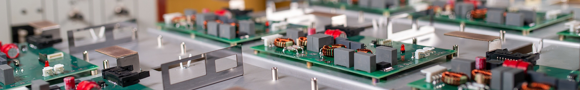
Multi-Layer PCB refer to printed circuit board has more than two copper layers, such as 4L, 6L, 8L, 10L, 12L, etc. As technology improving, people can put more and more copper layers on the same board. Currently, we can produce 20L-32L FR4 PCB. By this structure, engineer can put trace on different layers for different purpose, such as layers for power, for signal transfering, for EMI shielding, for components assembly, and so on. In order to avoid too many layers, Buried Via or Blind via will be designed in multi-layer PCB. For board more than 8 layers, high Tg FR4 material will be popular than normal Tg FR4. More layers it is, more complex & difficult the manufacturing will be, and more expensive the cost will be. The lead time of multi-layer PCB is different from normal one, please contact us for a exact lead time. |
| Structure of Multi-Layer PCB |
|
| Please click here for immediate quotation online Please contact us for more information about the Multi-Layer Printed Circuit Boards. |
ISimply drop your email or phone number in the contact form, and we'll promptly provide you with a quotation.