EBest Circuit (Best Technology) Co.,Ltd
- +86-755-2909-1601
- sales@bestpcbs.com
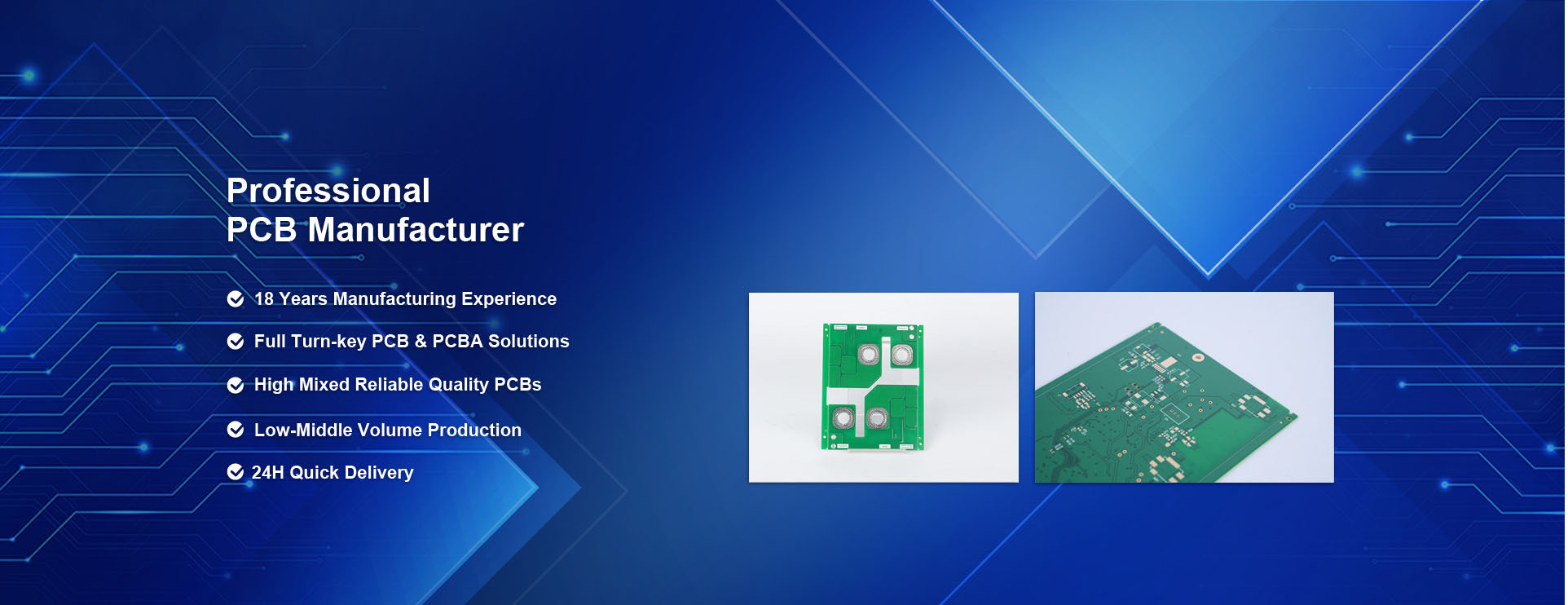
EBest Circuit (Best Technology) has offered high-quality PCBs and the best PCB assembly & box building service all over the world since 2006. We are professional fabricator on PCB prototype, IPC Class III standard are available. You can get high-quality PCB board and PCBA at a very reasonable price.
EBest Circuit (Best Technology) can manufacture your PCB and have it expedited to you within 24 hours. Providing full turn-key PCB manufacture includes extra thin PCB, HDI PCB, high TG PCB, RF PCB, rigid flex PCB, bus bar PCB, IC-substrate.
Our products ranging from standard FR4 PCB, multi-layer PCBs, metal-based PCBs (MCPCBs), ceramic PCBs, flexible and rigid-flexible PCBs to high frequency PCBs. Currently our mouthy capability is 260,000 square feet (28,900 square meter), more than 1,000 different boards will be completed. We also provide expediate service, so that urgent boards can be shipped out within 24 hours.
At a custom printed circuit board manufacturer, we believe that continuous growth is the key to success. So, we always invest much in research and development to stay ahead of industry trends. Our focus on product quality and customers satisfaction, and we aim to build strong relationships and offer personalized support and solutions to our customers.

We passed relevant PCB quality certifications and RoHS compliant quality management system, followed strict quality control process, after sale service with 5years, let you no worries!
We provide PCB design, PCB layout, PCB prototype fabrication, PCBA and box build assembly services. Our R&D team has deeply research on PCB with special requirements such as supper heavy copper PCB, semi-flexible PCB (flex area is FR4), blind buried hole PCB, back drilling PCB, countersunk/counterbore hole PCB.

We are committed to offering high-quality PCB solutions at competitive prices. By optimizing our production processes and managing costs efficiently, we ensure that you get the best value for your investment.

At EBest Circuit (Best Technology), quality is our top priority. We perform strict quality control procedures cover every stage of production, from raw material selection, prototyping to final product testing.

Our all-in-one approach simplifies supply chain, shorten lead times, and improves communication efficiency. And we have one-on-one sales-assistant service to give you a wonderful experience work with us.

We understand the importance of meeting your project deadlines, and we offer online WIP updates to make sure you can keep track of the progress of your PCB product.
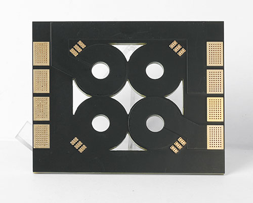
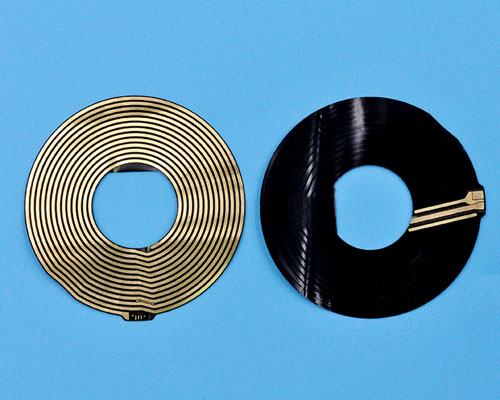
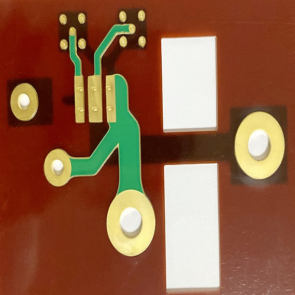
BEST ELECTRONICS MEMBRANE SWITCH
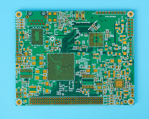
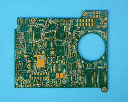
FR-4, is a widely acceptable international grade desination for fiberglass reinforced epoxy laminated that are flame retardant (self extinguishing). After add copper layer on one or each side FR4, it become to Copper Clad Laminate (CCL), and this is the non-conductive core materail for normal printed cricuit board (PCB). Printed circuit board using FR4 as core material will be named as "FR4 PCB".
PCB is used to mechanically support and electrically connect electronic components using conductive pathways, tracks or signal traces etched from copper clad laminate substrate. Sometimes, PCB also named Printed Wiring Board (PWB) or etching wiring board if no extra electronic components was added on.
Classification of FR4 Printed Circuit Board
According to number of copper trace layers, FR4 printed circuit board is normally divided into following types:
Single Sided (S/S), or Single layer;
Double Sided (D/S), or double layer, 2Layers, 2L;
Four Layers (4L), Six Layers (6L), Eight Layers (8L), Ten Layers (10L)
Board with more than 10L
In fact, for board more than four layers, people will named it "Multi-layer PCB". According to that standard, there're only three types of PCB: Single, Double and Multi-layers.
If divide the board according to manufacturing technology, major based on hole diamter size, it'll divid into two types:
Normal through hole (diameter >=0.20mm (8mil)
HDI (diameter <=0.15mm (6mil)
According to copper thickness, it can be divided into
Normall copper: copper thickness: 0.5 OZ, 1.0 OZ, 2.0 OZ,
Heavy copper: copper thickness: >= 3 OZ
According to core material, it can be divided into
Rigid FR4 PCB: Only FR4, it is rigid for whole board;
Rigid-flex circuits: Rigid FR4 plus flexible circuits;
According to Tg value of FR4, it can be divided into
Normal Tg: Value 130, 135, 140;
High Tg: Value 170, 180;
According to radio frequency (RF) level of PCB, it can be divided into
Normal: < 300 Mhz
High Radio Frequency: 300MHz ~ 3GHz,or even bigger
According to board thickness, it can be divided into
Normal: >=0.30mm
Extra Thin: 0.10~0.30mm;
As we know, the extra thin PCB means the thickness of printed circuit board is more thin than normal PCB, which is refer to a thickness smaller than 0.4mm for 1L/ 2L & 4L PCB. For extra thin PCB, we know they are all very thin and are easily to be broken, so the option for the surface treatment of the extra thin PCB is very crucial.
So, what kind of finishing to be recommended for the extra thin Rigid PCB?
Generally, there are 3 kinds finishing can be recommended for the extra thin PCB. It is OSP, ENIG (Electroless Nickel Immersion Gold), and ENEPIG.
But you may want to ask that lead-free Tin is also a common finishing for the PCB. Why not recommend LF HASL?
That’s because while LF HASL Process, the PCB will be easy to be blew away, people will use heated compressed air to leveling (blowing) on the coating molten tin (lead) solder, during this process, the traces will be easy to be broken as well.
So normally, we will not recommend the LF HASL finishing for an ultra thin FR4 PCB.
HASL lead-free is only suitable for a board with minimum thickness of 0.6mm, while the standard gold immersion surface coating can support PCB with a minimum thickness of 0.2mm. For the surface treatment of ENEPIG , which plate only needs to be about 0.1 microns for palladium and about 0.1 microns for gold, (palladium is a precious metal that is much harder than gold), so for board with ENEPIG finishing, its surface will looks more smooth, that’s also why it is the most recommended surface treatment for an extra thin PCB.
If you are searching for an extra thin PCB, feel freely to ask or send your inquiry to us. We will be pleased to share you more information regarding the extra thin PCB.
If you’ve ever made a pie with your kids, you know that the thickness of your crust is important. Too thin, and the pie falls apart into a mess of filling. Too thick, and you might as well be chewing on a loaf of bread. Getting the thickness just right is what makes a pie worth eating.
Even though PCB substrate materials are non-conductive and do not carry current, the board material still affects the electrical performance. FR4 PCB substrate is widely used, and a thorough understanding of this material is very necessary.
FR4 Thickness Design Considerations
If you start your design process by choosing the correct board thickness, you will avoid to redesign later. A number of factors are influenced by the board thickness. Before you start designing your board, think about the following design issues:
Form factor and flexibility: Does your PCB have a strict form factor requirement? Thinner boards tend to be used in smaller devices and can flex more than a thicker board. A more flexible board may be unusable with a pick & place machine. Electrical connections in flexible boards can also break unless they have some mechanical support.
Components and connections: Will the device have any components that require the Printed Circuit Board to have a specific thickness? Components like USB edge connectors and some through-hole components require PCB in correct thickness. BGA connectors generally require thicker boards.
Impedance matching: Traces on adjacent layers in multi-layer boards form a capacitor, and the layer thickness and its dielectric constant determines the equivalent capacitance. Impedance matching is critical, and the capacitance must be taken into consideration when designing the board. This is especially true in HDI PCB.
High-speed devices: If you are working with a high-speed device, FR4 is always not the best option, and some other material should be used instead. FR4 PCB could be used in high-speed devices when the layers are coated with high-speed laminates. These laminates offer significantly improved electrical performance over standard FR4, and generally a combination of FR4 and a high-speed laminate may be preferable to an alternative material.
RF losses: FR4 tends to have higher losses than other PCB materials that are specialized for RF applications. Traces on FR4 will have larger attenuation at RF frequencies than other specialized materials for a given board thickness. The board thickness also changes the effective dielectric constant of the board, which then changes the required impedance matching in RF circuits.
Thermal and Reliability Considerations
All materials expand at higher temperatures, and the thermal expansion coefficient must be taken into consideration when choosing the board thickness. The thermal expansion coefficient of FR4 changes drastically above the material’s glass transition temperature (140℃). The board can become electrically and mechanically unstable when the board operates above the glass transition temperature.
The reliability of the trace materials, laminate materials, and solder joints on a PCB laminate are determined by the resistance to thermal cycling. When the thermal expansion coefficients of the different materials are mismatched, fatigue occurs after repeated thermal cycling. Copper plating in vias and solder balls are especially vulnerable to damage under thermal cycling.
This is a greater problem in thick FR4 PCB with high aspect ratio vias. Plating damage in through-hole vias, lifted pads, and cracked surface resin can occur under the stress caused by thermal cycling. A thicker board will have a larger expansion magnitude for a given via aspect ratio, resulting in more damage to the board and the electronic components. Thermal stresses can be huge when an FR4 PCB runs above the glass transition temperature.
Volumetric expansion is also critical in rigid-flex FR4 PCB. Thermoplastic adhesives with low glass transition temperatures and high Z-direction expansion coefficients can exhibit very large volume expansion at high temperature. Z-direction expansion in these situations can be as large as 500 ppm/ƒ.
Even though a thicker FR4 PCB has greater thermal mass and can dissipate more heat from electronic components, there is also the potential for more damage due to thermal expansion. Therefore, how to choose between a thick and thin FR4 PCB that satisfies all other requirements, the thinner board may be a better choice if the FR4 PCB will undergo thermal cycling frequently.
If you work in Printed Circuit Board industry, you may know a normal PCB FR4-Tg is 130-140 degrees, the medium Tg is greater than 150-160 degrees, and High-TG FR4 Printed Circuit Board is greater than 170 degrees.
And what is a High-TG FR4 Printed Circuit Board? High-TG PCB is another name for a high-temperature FR4 PCB, it means the printed wiring boards designed to endure for extremely high-temperature. A Printed Circuit Board is defined as high-TG FR4 PCB if its glass transition temperature (TG) is higher than 170 degrees Celsius. High-TG FR4 will have better mechanical and chemical resistance to heat and moisture than standard FR4. The higher the TG value, the better the temperature resistance of the material, so High-TG FR4 is more and more popular particularly working in high power industry.
EBest Circuit (Best Technology) can provide many different High-TG FR4 material for Rigid Circuit board, Typical High-TG FR4 PCB material including: ITEQ-IT-180A, ISOLA 370HR, ShengYi S1000-2 and etc.
From the following PCB picture, you can see the normal TG130 FR4 PCB substrate is not only softening, deformation, melting, as well as other phenomenon working under high temperatures, but also there is a sharp decline in electrical properties, which will effect on product life.
If your FR4 Printed Circuit Board or PCBA board appear to above problems, then you should consider to use a High-TG FR4 Rigid Circuit Board. it may be catching your interest willing to understand a little bit more about High-TG FR4 printed circuit boards. Because High Tg Rigid Circuit board have a better stability at high temperatures, the substrate provides better heat resistance, mechanical and chemical stability for the circuit board.
Properties/ Applications of high Tg PCB
With the rapid development of electronics industry, High-TG FR4 PCB is widely used in Uninterrupted Power Supply, precise instrument as well as industry. High-TG FR4 PCB material probably designed for the high functionality, high multi-layer development high-density circuit; higher heat resistance and high-density surface mounting technology (SMT). So, the demand on High-TG FR4 PCB material become more widely used PCB manufacturing.
What’s more, High TG material is also popular in LED lighting industry, because heat dissipation of LED is higher than normal electronic components, but same structure of FR-4 board is much cheaper than metal core PCB, such as aluminum PCB.
High-TG FR4 PCB materials have the following properties:
 Resistance to high temperatures
 Long delamination durability (aging of materials to consider for safety reasons)
 Low thermal expansion
Excellent PTH reliability
Good mechanical properties
High temperature durability
High value of thermal stress resistance
high temperature durability
long delamination durability
Low Z axis expansion (CTE)
Advantages of High-TG FR4 PCB
Higher stability:Â it will automatically improve the heat resistance, chemical resistance, moisture resistance, as well as stability of the device if increasing the TG of a printed circuit board substrate.
Bear high power density designs:Â high TG PCB will be a good solution for heat management if the device has high power density with quite high heat generation rate.
It can achieve with using a larger printed circuit board to change the design and power requirements of a device when reducing the heat generation of ordinary board, what’s more, it also can use the high TG PCB.
Ideal for multilayer & HDI PCBs:Â there will lead to high levels of heat dissipation because multilayer & HDI PCBs are more compact and have dense circuits. So high TG PCBs are often used for the multilayer & HDI PCBs so that it can make sure reliability in Printed circuit board fabrication.
If your applications are in any danger of subjecting your PCBs to extreme temperatures or the PCB is required to be RoHS Compliant, it will be in your best interest to look into high-TG FR4 PCBs.
Come to contact EBest Circuit (Best Technology) Co., Limited. for High-TG PCB assistance. we can help you determine if you need high-temperature printed circuit boards and direct you to which specific boards are likely to be useful for your design and application. If you are transitioning to RoHS or just need more information about the High TG laminates, just give us a call and we’ll be happy to accommodate you. contact us online right now.
ISimply drop your email or phone number in the contact form, and we'll promptly provide you with a quotation.