PCB manufacturing PCB manufacturing
Home > Blog

Metal Core PCB

What Should You Specify When Ordering an LED ALU PCB?
Thursday, September 10th, 2026

An LED ALU PCB is an aluminum-backed metal-core circuit board that carries LEDs while moving heat toward a housing or heat sink. Ordering one by outline, wattage and quantity alone leaves the most important decisions undefined. Project teams should specify the dielectric, copper, aluminum base, LED footprint, mounting interface and acceptance tests as one thermal and mechanical system.

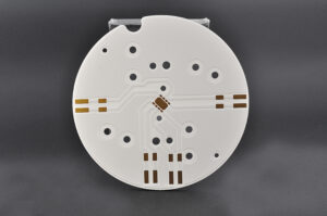
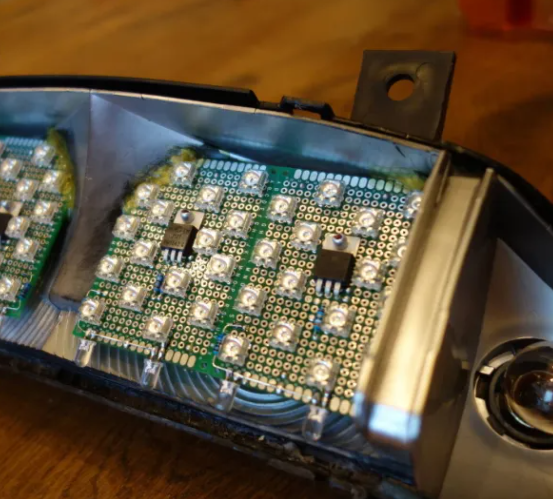
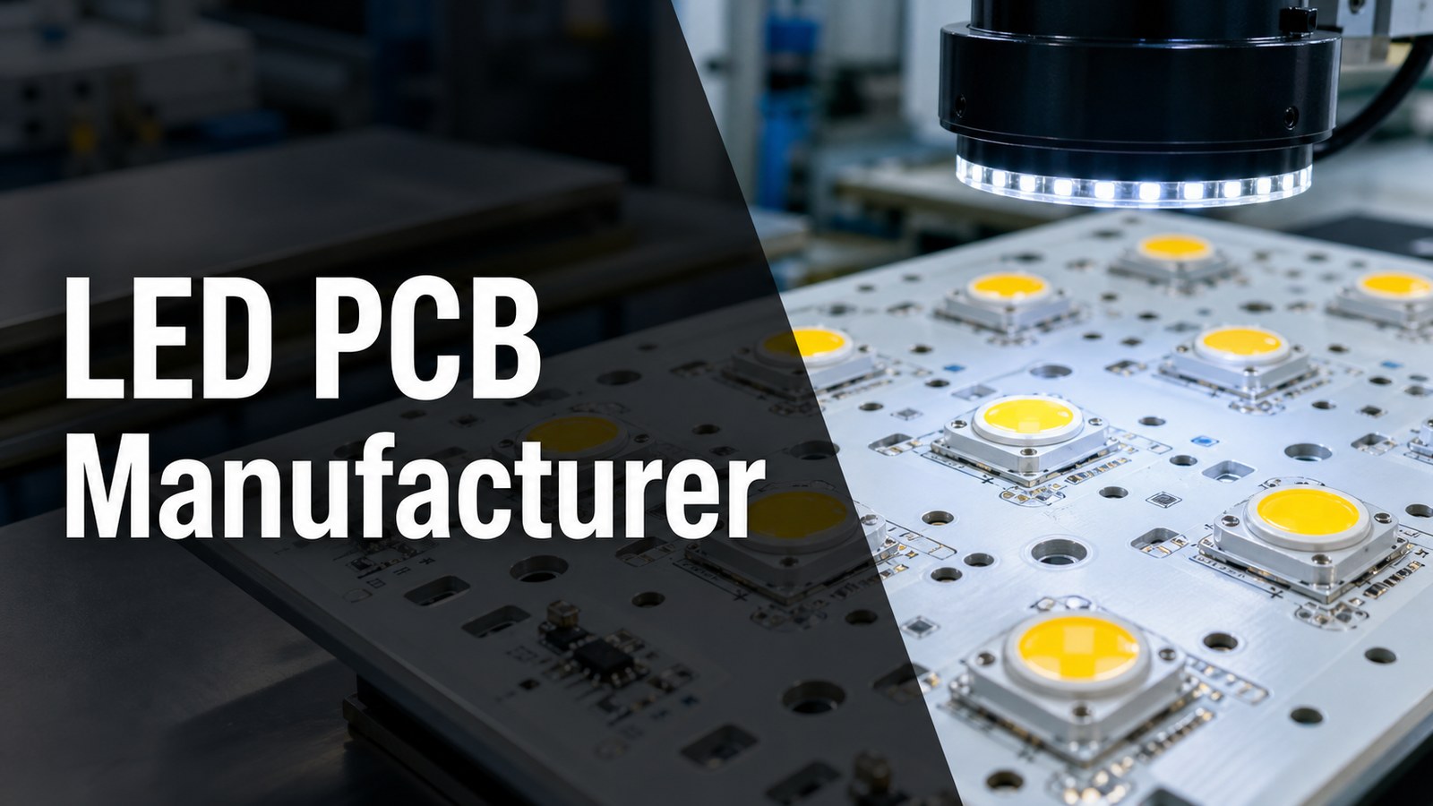
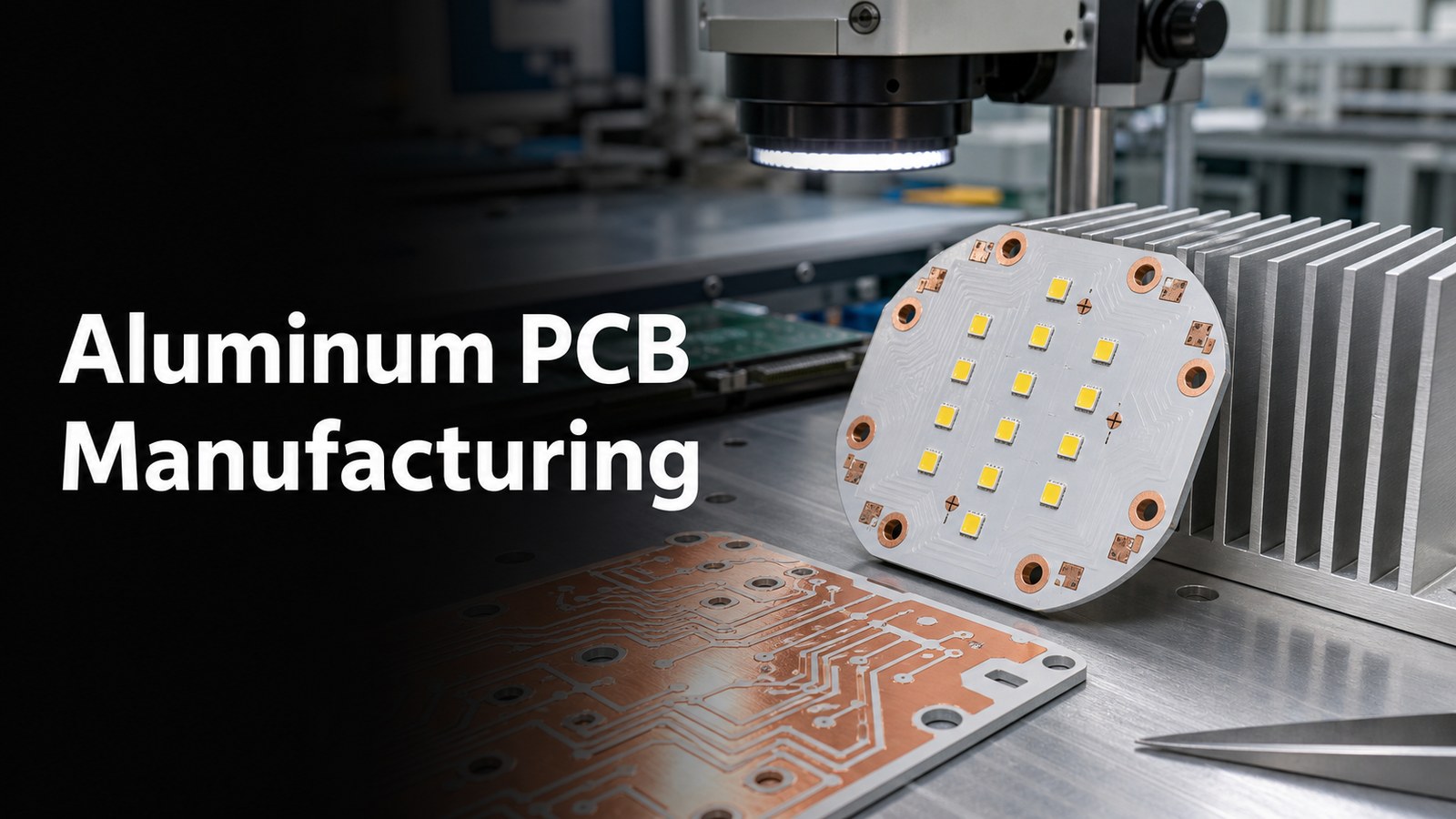
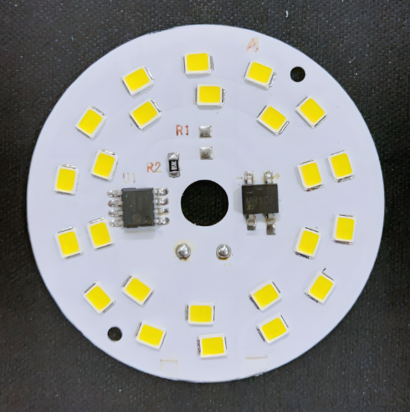
White LED aluminum PCB mounted on a machined aluminum heat sink during inspection

What Is an LED ALU PCB?

An LED ALU PCB, also called an LED aluminum PCB or LED MCPCB, normally has a copper circuit layer, a thin thermally conductive electrical insulator and an aluminum base. The LEDs are soldered to the copper pads. Heat then crosses the dielectric and spreads through the metal base before reaching the product’s heat sink or housing.

The aluminum is normally a thermal and structural layer, not an exposed circuit conductor. Copper features must remain electrically isolated from the metal base according to the design’s voltage requirements. This distinction also answers a common question, what is PCB in LED lights: it is the circuit platform that connects and supports the LEDs, and in an aluminum construction it also forms part of the heat-transfer path.

When Should You Choose LED Aluminum PCB Instead of FR-4?

Choose aluminum when the LED power density, enclosure temperature or available cooling area makes heat removal through ordinary FR-4 copper difficult. A low-power indicator board may still work well on FR-4. A dense array for a streetlight, high-bay lamp or compact optical module is more likely to need a metal-backed construction.

Project condition Likely starting point Reason to verify
Low-power indicators with generous board area FR-4 Copper spreading and thermal vias may be sufficient
Moderate or high LED heat with direct heat-sink contact Aluminum MCPCB Shorter through-thickness thermal path at practical cost
Very concentrated heat flux or direct-thermal-path requirement Copper-core or SinkPAD construction Local hot-spot removal may matter more than board weight or cost
Electrical isolation plus demanding temperature stability Ceramic substrate Different insulation, thermal and mechanical trade-offs apply

Do not select a board only because aluminum conducts heat better than FR-4. The thin dielectric can dominate the board’s through-thickness thermal resistance, while the thermal interface material, mounting pressure and heat sink govern what happens after heat reaches the metal base.

Which LED Products Benefit from an Aluminum Core?

An aluminum core is useful when the PCB can make broad, repeatable contact with a cooler part of the product. Typical uses include street and tunnel lights, high-bay fixtures, downlights, automotive exterior lamps, architectural luminaires, UV equipment and compact medical or inspection lighting.

A long LED PCB strip can use an aluminum base when the strip mounts continuously to an extrusion. A round LED PCB module may bolt to a heat sink around its perimeter. A custom LED PCB board becomes valuable when LED position must match optics, mounting holes, connectors and the enclosure. In each case, the application section of the drawing should identify how the metal back contacts the final assembly.

How Does Heat Move Through an LED ALU PCB?

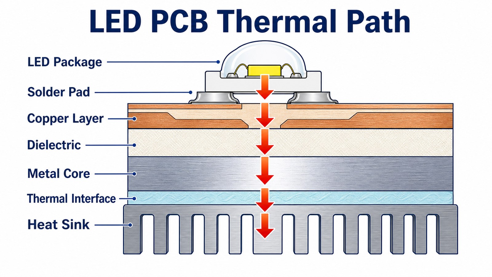
Heat starts at the LED junction and passes through the package thermal pad and solder joint into the PCB copper. It then crosses the thermally conductive dielectric, spreads into the aluminum base, crosses the thermal interface material and enters the heat sink or metal housing. Airflow and the outside environment finally remove that heat.
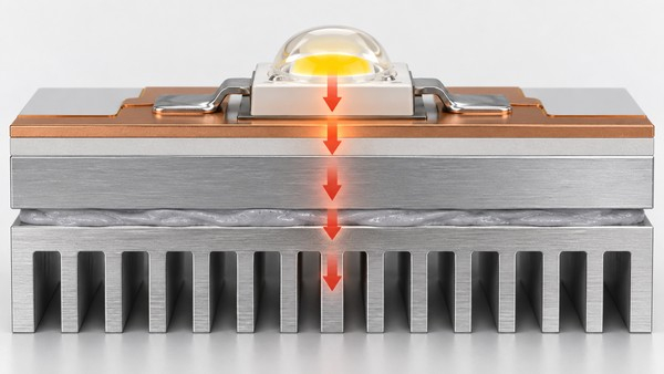
Cross-section showing heat moving from a high-power LED through copper dielectric aluminum base and thermal interface to a heat sink

Every interface adds thermal resistance. A high-conductivity laminate cannot compensate for a voided LED solder joint, a warped board, dry contact against the heat sink or an undersized enclosure. Thermal design should therefore start with an allowable LED junction or case temperature and work backward through the complete junction-to-ambient path.

Which Material and Stack-Up Specifications Control Performance?

The quotation package should identify the values below or ask the manufacturer to propose them against defined operating conditions. A single thermal-conductivity number is not a complete stack-up.

Specification What it controls What the project team should provide
Dielectric thermal conductivity How readily heat crosses the insulating layer Target or approved material family and thermal objective
Dielectric thickness Thermal resistance and electrical-isolation margin Required withstand voltage, safety spacing and test condition
Copper thickness Current capacity, lateral heat spreading and etching limits LED and driver currents plus minimum finished copper
Aluminum base thickness Stiffness, heat spreading, weight and mechanical fit Finished board thickness and enclosure constraints
Board flatness and outline tolerance Heat-sink contact and optical alignment Datum scheme, mounting features and critical dimensions
Surface finish and solder mask Solderability, pad protection and optical appearance Assembly process, exposed-pad needs and approved color

We support MCPCB dielectric options with thermal-conductivity values of 0.8-1.0, 1.5, 2.0 and 3.0 W/m·K. These values describe the dielectric option, not the thermal conductivity of the complete assembled lamp. Final material availability and performance remain subject to the released stack-up, board dimensions, quantity and engineering review.

Which LED MCPCB Structure Should You Order?

A single-layer MCPCB is the practical starting point for many LED plates because the circuit sits on one side and the exposed metal back can contact the heat sink. It offers the shortest and simplest manufacturing path when all LED routing fits on one copper layer.

A two-layer MCPCB adds routing capacity on the component side through an additional circuit layer and dielectric construction. A double-sided structure places circuitry on both outer sides around the metal core and requires a different interconnection strategy. Multilayer constructions are possible, but the added insulation and fabrication complexity must serve a real routing or integration requirement.
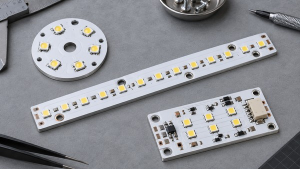
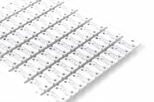
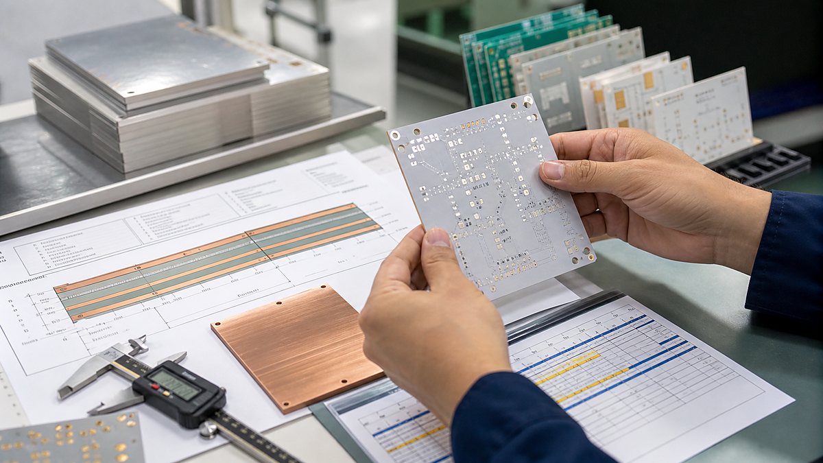
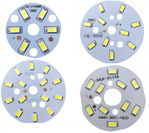
Round strip and rectangular custom LED aluminum PCB formats on an engineering workbench

For tightly concentrated heat, a SinkPAD direct-thermal-path board may be more appropriate than a conventional metal core PCB for LED. It is not an automatic upgrade for every lamp. The LED package, thermal pad geometry, electrical isolation requirement and assembly process must be compatible with the selected construction.

How Should the LED Footprint, Copper and Polarity Be Designed?

An effective LED PCB board design begins with the package manufacturer’s land pattern and thermal-pad guidance. The exposed thermal pad should have controlled solder-paste coverage, while anode and cathode markings must remain clear after assembly. Footprints copied between LED families can create solder or optical-position errors even when the package outline looks similar.

  • Place LEDs for both optics and heat spreading: avoid unnecessary clustering unless the cooler is designed for the resulting hot spot.
  • Size current paths from the real drive current: include shared return paths, connectors and any on-board driver components.
  • Use copper area deliberately: it spreads heat laterally before heat crosses the dielectric, but should not violate optical or creepage requirements.
  • Define polarity in all production files: align silkscreen, centroid rotation, assembly drawing and test instructions.
  • Keep mounting hardware clear of live copper: mounting holes, washers and metal housings need appropriate electrical clearance.

For an SMD LED PCB board, provide the BOM and centroid data when assembly is required. LED bin, color temperature, wavelength, luminous flux and forward-voltage constraints belong in the approved sourcing specification rather than in informal email notes.

How Should the Board Mount to the Heat Sink?

The aluminum back must meet a flat, clean mating surface through a controlled thermal interface material. Define the TIM type and thickness, screw locations, torque method, clip force or adhesive system before prototype approval. Mounting pressure should be distributed so the board remains flat without damaging the dielectric or solder joints.

Place mounting points close enough to control lift around hot zones, but do not crowd LED optics or copper clearances. If the board sits in an aluminum enclosure, include coating, anodizing and grounding requirements in the mechanical review. Anodized surfaces and thermal pads have electrical behavior that should be verified rather than assumed.

Which Surface Finish and White Solder Mask Fit LED Assemblies?

Surface finish should match the assembly process, pad geometry, storage plan and any wire-bond or exposed-contact requirement. ENIG, lead-free HASL, OSP and other finishes each have different flatness, cost and handling characteristics. The best choice is the one qualified for the actual component and production process.

White solder mask is common on visible lighting boards because it can support optical reflectance around the LEDs. Its color stability, coverage and curing must be controlled for the operating temperature and reflow process. White mask does not replace thermal design, and reflectance should be evaluated with the real optical system when it is a product requirement.

How Do We Manufacture and Assemble LED Aluminum PCBs?

At EBest Circuit (Best Technology), we review the Gerber data, stack-up, metal-base construction, outline, mounting plan and assembly files before release. Our MCPCB manufacturing capabilities cover single-layer, two-layer, double-sided and multilayer constructions up to 10 layers. Depending on the approved material and design, we can manufacture boards with 0.30-4.0 mm thickness, 0.15/0.15 mm minimum line/space and dimensions up to 100 × 1,300 mm. These maximum capabilities depend on material, stack-up, board dimensions, design complexity, quantity and engineering review.

Fabrication normally combines copper imaging and etching, dielectric-to-metal lamination, drilling or routing, solder-mask and surface-finish processing, profiling and electrical testing. If assembly is included, we can review the BOM and placement data, print solder paste, place SMD LEDs, control the reflow profile and perform inspection. Aluminum panels have different thermal mass from FR-4, so process settings must be developed for the actual panel and component limits.

What Inspection and Thermal Validation Should Be Defined?

Bare-board electrical testing checks opens and shorts, but it does not prove the finished lamp’s junction temperature or light output. The control plan should match the risks that matter to the customer.

  • Incoming material and stack-up verification: confirm the approved laminate, copper and finished thickness.
  • Dimensional inspection: check the outline, mounting holes, critical LED datums and flatness requirements.
  • Electrical test: verify continuity, isolation and any specified withstand-voltage condition.
  • Assembly inspection: use SPI, AOI or X-ray where the package and acceptance plan justify them.
  • Functional lighting test: define current, voltage, polarity, warm-up time and pass/fail limits.
  • Thermal validation: measure at agreed points in the intended mounting, ambient and duty-cycle conditions.

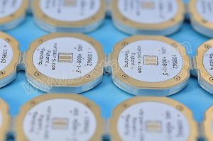
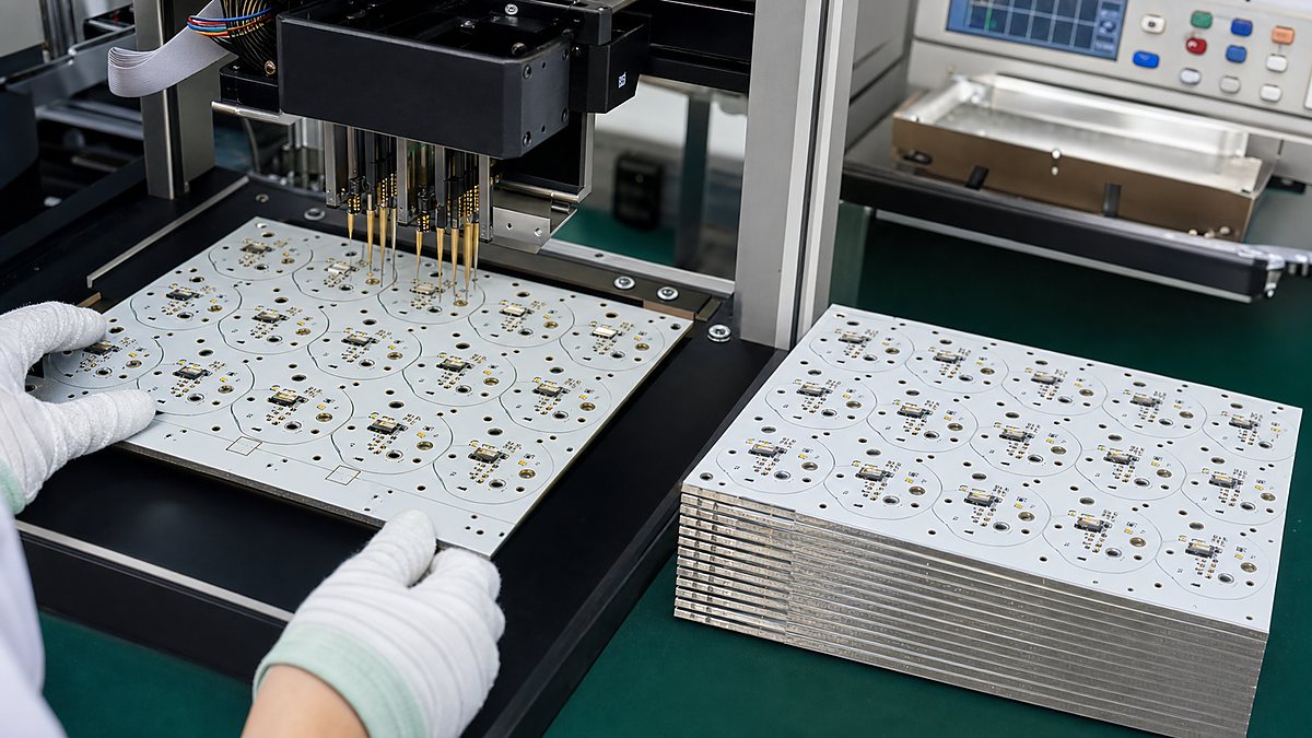
Technician inspecting assembled LED aluminum PCB panels with optical and thermal imaging equipment

We can support AOI, flying-probe or universal electrical testing, copper-thickness checks and final inspection as appropriate to the build. Product-level thermal or optical acceptance requires customer-defined conditions and limits; it should not be inferred from a bare laminate data sheet.

What Drives LED PCB Board Price and Lead Time?

LED PCB board price depends on panel utilization, board shape, copper and aluminum thickness, dielectric grade, layer count, surface finish, solder-mask requirements, test coverage and quantity. Irregular outlines, long strips and tight mechanical tolerances can affect tooling and material yield even when the electrical circuit is simple.

For suitable single-layer MCPCB orders, we can support lead times as fast as 24 hours after engineering review and material confirmation. We confirm the actual lead time according to material availability, tooling, assembly, testing and order volume.

What Should You Include in an Aluminum PCB for LED Build Package?

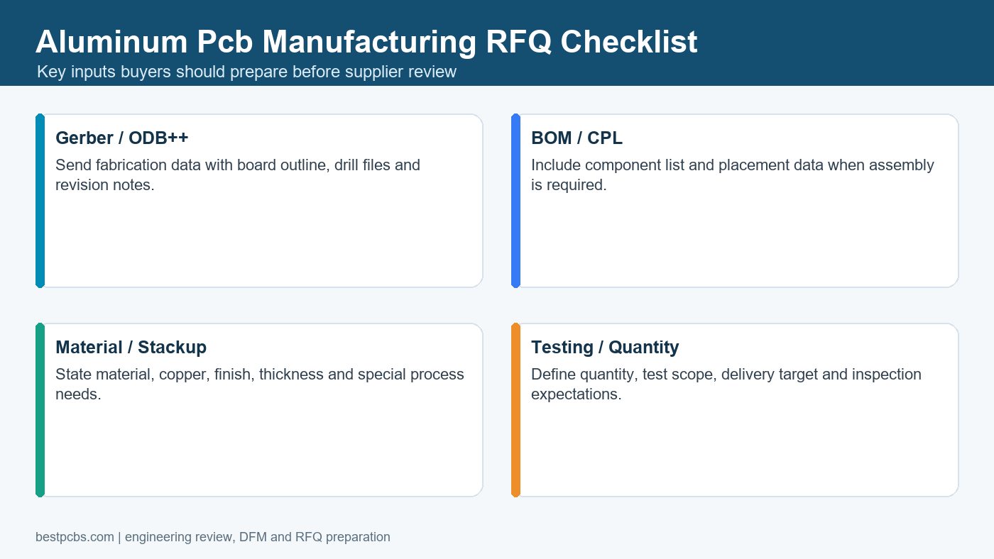
A complete aluminum PCB for LED quotation package lets suppliers quote the same construction and reduces late changes. Include:

  • Gerber or ODB++ data, fabrication drawing and stack-up;
  • finished board thickness, copper weight, dielectric requirement and aluminum-base requirement;
  • outline, panelization, mounting-hole details, flatness and critical dimensions;
  • surface finish, solder-mask color and any reflectance requirement;
  • LED power, current, operating ambient, duty cycle, heat sink and TIM description;
  • BOM, centroid file, assembly drawing and LED binning requirements when PCBA is included;
  • electrical, isolation, functional, optical and thermal test conditions;
  • prototype quantity, production forecast, packaging and traceability needs.

For an aluminum core PCB for LED, also identify where the bare metal may contact the enclosure and whether it must be grounded or isolated. For an aluminum PCB for LED light with optics, provide the LED-to-lens datums and allowable positional tolerance.

Frequently Asked Questions About LED ALU PCBs

What is an aluminum PCB?

It is a printed circuit board that uses a metal base, usually aluminum, beneath an electrically insulating dielectric and copper circuit. The metal spreads heat and adds stiffness while the dielectric keeps the circuit electrically isolated.

Does an LED aluminum PCB eliminate the heat sink?

No. It improves the path from the LED toward the cooler, but the TIM, heat sink, enclosure and airflow must still release the heat. Some low-power products use the housing itself as the heat spreader.

Can an LED MCPCB carry the driver circuit?

Yes, when routing density, voltage spacing and thermal conditions fit the selected structure. In many products, separating the LED plate from an FR-4 control board simplifies both thermal contact and dense routing.

Is higher dielectric conductivity always better?

Not by itself. Conductivity, dielectric thickness, isolation voltage, bond reliability, material availability and cost must be considered together.

Can the same board be used for different LED wattages?

Only after checking current paths, LED footprint, heat density, driver conditions and the full cooling assembly. Matching the outline does not prove thermal compatibility.

Send a Build-Ready LED ALU PCB Package

A reliable LED ALU PCB order starts with the complete thermal path, not a material name alone. Send your Gerber files, stack-up, BOM and placement data, mechanical drawing, operating conditions and test requirements to sales@bestpcbs.com. We will review the construction and identify the points that need confirmation before prototype or production release.
You may also like

EV Charger MCPCB Manufacturer | Custom Fabrication & Assembly
Tuesday, September 8th, 2026

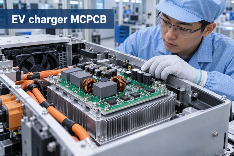
An EV charger MCPCB helps move heat away from switching devices, rectifiers, power resistors, and auxiliary power circuits as charging systems become smaller and more powerful. An MCPCB can move that heat into a chassis, heat sink, or cold plate more efficiently than a conventional board—but only when the board is designed as part of that thermal path.

EBest Circuit manufactures custom aluminum- and copper-base PCBs and provides component sourcing, assembly, and testing. We help charger developers match the board construction to the module instead of treating every PCB inside an EV charger as a metal-core board.

EV charger PCB is a broad term. EV charging PCB and electric vehicle charging PCB can refer to several different boards across the charging system. In this article, EV charger MCPCB means a metal-core board used within a defined power or thermal module—not every PCB in the system.

EV charger MCPCB

Where Does an MCPCB Fit Inside an EV Charger?

An MCPCB fits where heat is concentrated and there is a short, controlled path from the component to a metal cooling surface.

In an EV charger, that can include a compact power conversion board, a rectifier section, an auxiliary power module, or a board carrying high-loss switching devices. It can also be used for high-power status lighting. The metal base spreads heat beneath these components and transfers it toward the charger housing, a heat sink, or a cold plate.

It is usually not the first choice for communication, metering, display, or central control boards. Those boards often need multilayer signal routing, controlled impedance, dense interconnections, or isolation between several electrical domains. FR-4, heavy-copper PCB, insulated metal substrate, ceramic, and hybrid structures each solve different problems.

Application labels also need clear boundaries. An EVSE PCB belongs to stationary charging equipment, while an on-board charger PCB, or OBC PCB, operates inside the vehicle. A DC fast charging PCB may describe a control board, gate-driver board, or power-module board with very different construction needs. An EV charger control board is usually not an MCPCB unless it also carries concentrated heat into a defined cooling surface. Supplier listings may use the phrase EV charging board PCB, but that wording is too broad to specify the correct board technology.

The practical dividing line is simple:

  • Use an MCPCB when the PCB must conduct heat into a defined cooling surface.
  • Consider another construction when routing density, high-voltage spacing, or complex multilayer connections dominate the design.

That distinction keeps the thermal board focused on the part of the charger where it creates measurable value.

When Does EV Charger PCB Design Require a Metal Core?

Choose a metal core PCB for EV charging when temperature cannot be controlled reliably through copper area, thermal vias, airflow, and a conventional laminate alone.

This often happens when several conditions appear together: high component loss, limited board area, restricted airflow, and direct mechanical contact with a heat sink or enclosure. In that situation, the metal base becomes a heat-spreading layer rather than simply a stronger board material.

For example, a power semiconductor may operate safely on FR-4 at a moderate load but exceed its temperature target when the same circuit is packaged into a smaller charger. Moving to an MCPCB can shorten the heat path. The result depends on the entire structure—from the component pad and copper circuit through the dielectric layer and metal base to the external cooling surface.

A metal core is less useful when the main limitation is elsewhere. It will not correct an undersized heat sink, poor board-to-housing contact, excessive semiconductor loss, or insufficient airflow. It may also complicate a design that needs many signal layers or long high-voltage creepage paths.

The choice should therefore be based on the module’s losses, allowable temperatures, mechanical interface, and insulation requirement—not on charger power alone.

Which PCB Material Fits Your EV Charger Application?

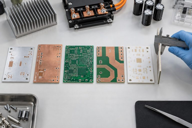
The right material depends on the job of the board. An EV charger normally uses more than one PCB technology because heat transfer, current carrying, signal routing, isolation, and mechanical requirements do not peak in the same place.

  • Aluminum MCPCB fits cost-sensitive thermal modules that need to spread component heat into a housing or heat sink. It is a practical choice when the layout is relatively simple and aluminum can keep the hot spots within the temperature target.
  • Copper-base MCPCB fits smaller or more demanding thermal modules where heat is highly concentrated and stronger lateral heat spreading is needed. It can improve the path away from a power device, but it also increases material cost and board weight.
  • High-Tg FR-4 fits control, communication, sensing, and multilayer power-control boards that need routing density, plated through-holes, and high-voltage separation. Its higher glass-transition temperature improves dimensional and thermal stability, but High-Tg does not mean high thermal conductivity.
  • Heavy-copper PCB fits high-current distribution, terminals, relays, and power paths where conductor temperature rise is the main concern. It carries more current and adds thermal mass, but it does not provide the same direct board-to-heat-sink path as an MCPCB.
  • Ceramic PCB fits compact modules that need strong electrical insulation, high-temperature stability, low expansion, or high thermal performance. It can be valuable around demanding power devices, but cost, size, brittleness, copper attachment, and assembly handling must be considered.

Many chargers need a mixed solution rather than one material throughout the product. For example, a High-Tg FR-4 control board can manage communication and safety functions, a heavy-copper board can distribute current, and an aluminum, copper-base, or ceramic board can support the most concentrated thermal load.

Use the dominant engineering problem as the first filter:

  • heat must move into a chassis or heat sink → aluminum or copper-base MCPCB;
  • high current must travel across the board → heavy-copper PCB;
  • multilayer signals and isolation dominate → High-Tg FR-4;
  • high temperature, insulation, and dimensional stability dominate → ceramic PCB.

Final selection still depends on operating voltage, loss distribution, cooling design, board size, production quantity, and target cost. A material comparison is useful only when it is tied to the actual EV charger module.

EV charger MCPCB

What Thermal Management Risks Should Be Checked in an EV Charger MCPCB?

The main risk is assuming that a high thermal-conductivity material automatically produces a cool, reliable assembly. Heat must cross several interfaces, and the weakest one can control the result.

  • A thick dielectric layer can restrict heat flow. It may provide stronger isolation, but it also increases thermal resistance. The correct balance depends on operating voltage and heat density.
  • A high average board temperature can hide local hot spots. Temperature should be checked beneath the switching device and at its thermal pad, not only at the edge of the board.
  • Poor contact can cancel the benefit of the metal base. Board flatness, interface material, screw position, mounting pressure, and heat-sink finish affect real performance.
  • Copper geometry affects both current and temperature. Narrow current paths, connector transitions, or insufficient copper around a power device can create additional heat before it reaches the base metal.
  • Thermal cycling creates mechanical stress. Different expansion rates among components, solder joints, copper, dielectric, and metal base can reduce long-term reliability.
  • Electrical isolation cannot be traded away for lower thermal resistance. Dielectric withstand, creepage, and clearance remain essential in charger hardware.

A useful thermal review follows the heat from its source to the final cooling surface. It does not stop at the MCPCB datasheet value.

What Should Buyers Specify for DC Fast Charging Boards?

For DC fast charging, buyers should first specify the function of the board. A control PCB, gate-driver board, power module, and communication board experience different voltage, current, heat, and isolation conditions.

For the MCPCB itself, the most influential requirements are:

  • operating and peak current;
  • voltage and dielectric withstand requirement;
  • expected component losses and hot-spot locations;
  • aluminum or copper base;
  • dielectric thickness and thermal performance;
  • copper weight and critical current paths;
  • finished thickness, flatness, and mounting tolerances;
  • connection to the heat sink, housing, or cold plate;
  • operating environment and temperature range.

These details matter more than requesting the “highest thermal conductivity.” A thinner dielectric may improve heat transfer but must still meet isolation needs. A copper base may spread heat effectively but can add unnecessary cost and weight if an aluminum base already meets the temperature target.

Buyers should also define whether the order covers bare boards or completed assemblies. If components, thermal interface materials, busbars, connectors, or heat sinks are part of the build, they should be considered together because they change the assembly process and final thermal path.

How Should EV Charger PCB Assembly Be Qualified?

An EV charger PCBA should be qualified by proving that the assembled module performs as intended under representative electrical, thermal, and mechanical conditions. This is the practical purpose of EV charger PCB assembly qualification.

Start with the failures that matter to the product. A power board may need confirmation of current handling, isolation, temperature rise, and solder integrity. A module attached to a housing may also need verification of flatness, contact pressure, connector alignment, and repeated thermal cycling.

Inspection methods should match the assembly:

  • AOI can verify polarity, placement, and visible solder joints.
  • X-ray can examine solder beneath power packages and thermal pads.
  • Electrical tests can check continuity, isolation, and withstand performance.
  • Functional testing can confirm that the module operates at its intended load.
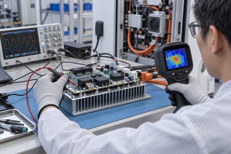
  • Temperature measurements can reveal whether heat reaches the cooling surface without an excessive local hot spot.

The prototype should be tested in a realistic mechanical setup. Testing a loose board on a bench cannot represent a design that relies on a chassis or cold plate. Once the module passes, the approved material, stack-up, component revision, mounting method, and test limits should remain consistent for repeat production.

EV charger MCPCB

How Do You Choose an EV Charger Circuit Board Manufacturer?

Choose an EV charger PCB manufacturer that understands both sides of the project: how to build the metal-core board and how that board functions inside the charger.

A capable supplier should be able to explain why the proposed base metal, dielectric, copper weight, surface finish, and assembly process fit the module. If a different PCB construction would serve the application better, the supplier should identify that before production rather than simply quoting the requested material.

Coordination also affects the result. When bare-board fabrication, component sourcing, assembly, and testing are handled separately, a thermal or soldering issue can fall between suppliers. A coordinated PCB and PCBA workflow makes it easier to connect material decisions with component packages, solder profiles, mechanical interfaces, and acceptance tests.

EBest Circuit supports prototypes, small batches, and repeat production through PCB manufacturing, component sourcing, PCBA, and testing. One business contact works with an engineering support team to coordinate technical questions. DFM review can identify conflicts involving the board structure, component spacing, panelization, assembly access, and testability before the build begins.

For programs that require formal quality controls, available certifications include ISO 9001, ISO 13485, IATF 16949, and AS9100D. The applicable production site, documentation, inspection level, and customer requirements should be confirmed for the individual project.

The strongest manufacturing partner is the one that reduces uncertainty before the prototype and preserves the approved solution when the project moves into repeat production.

Why Choose EBest Circuit as Your EV Charger Circuit Board Manufacturer?

EBest Circuit gives EV charger developers one coordinated route from a thermal-board concept to an assembled and tested product. Instead of separating the bare board, components, assembly, and engineering questions among several suppliers, customers work with one business contact supported by three engineers throughout the project.

This is especially useful for an EV charger MCPCB because the board material cannot be separated from the power package, solder joint, mounting surface, and cooling structure. Our engineering support connects these decisions before production:

  • DFM review covers the MCPCB structure, dielectric, copper, tolerances, panelization, component spacing, and test access.
  • PCB fabrication, component sourcing, PCBA, and testing can be managed as one project.
  • Prototype and small-batch support helps engineers check electrical operation, mechanical fit, and thermal behavior before repeat production.
  • A supply network of more than 1,000 partners supports component and material sourcing while our own PCB and PCBA factories coordinate production quality and timing.
  • Digital production records allow material and product batches, manufacturing progress, and production history to be traced quickly.

EBest Circuit has 20 years of PCBA experience and has served more than 10,000 engineers and 1,800 customers. Available quality-system certifications include ISO 9001, ISO 13485, IATF 16949, and AS9100D. The applicable factory, inspection plan, documentation, and certification requirements are confirmed according to the individual EV charging project.

For customers, the practical benefit is a shorter path from an engineering question to a build decision—and fewer gaps between MCPCB fabrication, assembly, thermal integration, and testing.

FAQs About EV Charger MCPCB

Does every EV charger need an MCPCB?

No. An EV charger may contain several board types. MCPCB is most suitable for a board that must transfer concentrated component heat into a metal cooling structure.

Is aluminum or copper better for an EV charger MCPCB?

Aluminum is often sufficient for cost-effective heat spreading. Copper can spread heat more aggressively but adds cost and weight. The right choice depends on losses, board size, cooling design, and temperature targets.

Does higher thermal conductivity always produce a cooler board?

No. Dielectric thickness, copper layout, component attachment, interface material, mounting pressure, and the external heat sink can have as much influence as the published conductivity value.

Can one supplier manufacture and assemble the board?

Yes. Combining fabrication, component sourcing, PCBA, and testing can reduce handoff risks, especially when power packages, thermal pads, heavy connectors, or a defined cooling interface are involved.

What should a prototype prove?

It should prove electrical operation, isolation, temperature behavior, solder quality, mechanical fit, and contact with the intended cooling surface under representative conditions.

Can an approved prototype move directly into repeat production?

It can move forward after the material, stack-up, components, assembly method, mechanical interface, and acceptance limits are frozen. Any later substitution should be reviewed for electrical, thermal, and mechanical impact.

Need a custom EV charger MCPCB for a power or thermal module? Send your Gerber files, BOM, board drawing, operating conditions, quantities, and testing needs to sales@bestpcbs.com. EBest Circuit can review the construction and provide a coordinated fabrication and assembly quotation.

You may also like

Metal Core PCB Manufacturers in Spain: Companies, Capabilities and Sourcing Options
Wednesday, September 2nd, 2026

Metal Core PCB manufacturers in Spain include CIRLAN, Fast PCB, Maxwell Atlantic and CIPSA Circuits. The useful differences are practical: which IMS structures they describe, what quality controls they disclose, whether they publish a lead time, and whether they supply only bare boards or can cover a wider manufacturing scope.

If you are sourcing an aluminium or copper-base PCB, start with the structure and delivery requirement. A single-sided lighting board, a double-sided PTH IMS design and a fully assembled thermal board do not belong in the same RFQ. The comparison below shows what each supplier publicly offers and which details still need a written quotation.

Metal Core PCB manufacturers in Spain, aluminium and copper IMS panels in a quality inspection lab

Who Are the Main Metal Core PCB Manufacturers in Spain?

CIRLAN, Fast PCB, Maxwell Atlantic and CIPSA Circuits all identify finished PCB manufacturing operations in Spain and publish an IMS or metal-core offer. Their process scope and delivery visibility are not the same.

Company Process capability Lead-time information Service scope
CIRLAN
Urnieta, Gipuzkoa
Single-sided aluminium and copper IMS; published standard and special dimensional ranges No standard IMS turnaround published; factory route and committed date belong in the quote Engineering, optimisation, panelisation and bare PCB manufacturing; some technologies may use Shenzhen partners
Fast PCB
Irún, Gipuzkoa
Single-sided aluminium IMS; 0.8–3.2 mm base, 35–105 µm copper and 100 m²/day stated capacity Short series: 5 working days
Large series: 10 working days
Bare PCB prototypes and series; routing, V-scoring, chemical tin and optional production certificate
Maxwell Atlantic
Santiago de Compostela
Aluminium or copper IMS within an in-house single-, double- and multilayer PCB process No standard IMS turnaround published; ask for prototype and repeat-order dates separately Bare PCB manufacturing for prototypes and small, medium or large series; in-house inspection and traceability
CIPSA Circuits
Rubí, Barcelona
Aluminium IMS, including single-sided, isolated-hole, double-sided and PTH structures General PCB prototype service: 24 hours to 5 days; confirm that the quoted IMS build qualifies Bare PCB prototypes and series with process testing and lot traceability

Match the shortlist to the actual build before requesting prices. Fast PCB publishes defined timing for single-sided aluminium IMS; CIRLAN provides aluminium and copper single-sided process limits; CIPSA documents double-sided and PTH aluminium structures; and Maxwell Atlantic offers broad in-house PCB inspection and traceability. Send the same material, quantity, test, dispatch-date and delivery-price requirements to the relevant suppliers so their quotations cover the same work.

CIRLAN

CIRLAN publishes one of the clearest Spanish process windows for single-sided aluminium and copper IMS. Its aluminium range lists 1.0, 1.5, 2.0 and 3.0 mm board thicknesses. Standard copper is 35 or 70 µm; 105 µm is listed as special production. The same table gives track and spacing, drill, routing, scoring, panel-size and finish limits.

That detail helps a buyer see whether a conventional IMS design falls inside the standard column before requesting a quote. It does not publish a standard turnaround or price. Ask CIRLAN to identify the dielectric grade, thermal data, metal alloy, inspection package and dispatch date for the released files.

CIRLAN separates local services from outsourced technologies. Its local scope includes engineering, optimisation, panelisation, aluminium IMS and copper IMS. The company also describes cooperation with PCB factories in Shenzhen for other technologies. If Spain production is a purchasing condition, the quotation should name the physical plant for the exact part.

Fast PCB

Fast PCB is the easiest supplier in this group to assess when the project is a conventional single-sided aluminium board and delivery speed matters. Its IMS page states 5 working days for short series, 10 working days for large series and 100 m²/day of production capacity.

The published process range covers aluminium bases from 0.8 to 3.2 mm, copper from 35 to 105 µm, a maximum delivery format of 544 × 390 mm, chemical tin, CNC routing and V-scoring. That is enough to reject obvious mismatches before engineering spends time on an RFQ.

Fast PCB also describes a metallographic laboratory that performs ageing tests, thermal shock, digital microsection measurement and solderability checks. A production certificate can be supplied with the order on request. Put the required report, sampling level and acceptance criteria into the purchase specification; do not assume every report is included in the unit price.

Its public IMS offer is specifically single-sided aluminium. Copper-base, plated-through-hole, double-sided IMS and alternative finishes need an explicit technical answer and separate schedule.

Maxwell Atlantic

Maxwell Atlantic is relevant when a buyer wants broad in-house PCB process control as well as an aluminium or copper IMS option. The Santiago de Compostela company states that its PCB manufacturing is carried out without third-party subcontracting and can cover prototypes plus small, medium and large series.

Its listed equipment and processes include CNC drilling and milling, lamination, single-, double- and multilayer etching, electroplating, desmear, AOI, solder-mask processing, laser marking and flying-probe electrical test. The quality system follows UNE-EN-ISO 9001, and the company describes full traceability for raw materials and test results.

This is useful quality evidence, but the public pages do not provide an IMS-specific lead-time table or detailed metal-core process window. The quotation should therefore state the exact IMS structure, dielectric, thermal and isolation values, PTH method, inspection reports, quantity break and committed dispatch date. Ask for the IMS limits, not a general PCB capability list.

CIPSA Circuits

CIPSA Circuits publishes the widest aluminium IMS structure range among the four companies compared here. Its capability material covers single-sided boards, isolated holes, openings in the aluminium, double-sided PTH with an aluminium base and double-sided constructions with an aluminium core. Several structures list 35 or 70 µm copper and 0.15 mm line and spacing.

CIPSA states on its quality page that it performs rigorous controls throughout manufacturing and retains traceability for raw materials and test results. Its general prototype service runs from 24 hours to 5 days and uses the same production lines and finishes as series manufacture. Because that timing page covers PCB prototypes broadly, ask CIPSA to confirm whether the actual IMS material and construction qualify for the requested expedite window.

CIPSA is a strong technical candidate for aluminium IMS that goes beyond a basic single-sided board. Copper-core IMS, the current revision of the capability data, inspection deliverables, setup charges and freight to the final destination still need to appear in the quotation.

How Do These Metal Core PCB Manufacturers Compare?

Do not compare four unit prices until every quote covers the same material, tests, quantity, delivery point and service scope. A cheaper line item can become the expensive choice once tooling, certificates, freight or a second supplier for assembly is added.

Buyer concern What to compare What the quote should state
Quality IMS material identity, electrical test, isolation test, dimensional inspection, traceability and non-conformance handling Named material and factory, test method, sampling or 100% scope, reports supplied and acceptance criteria
Total price Unit price at prototype and repeat quantities, tooling, test reports, special material, packing, freight and import charges Separate line items, quotation validity, quantity breaks, Incoterm and currency
Lead time DFM response, material procurement, fabrication, test, packing and transit Clock start, working days, engineering-hold rule, dispatch date and arrival responsibility
Service scope Bare PCB only or PCB plus component sourcing, assembly, inspection, functional test and shipping Exact owner for each stage, included deliverables and warranty or failure-analysis route

Ask for two dates: the factory dispatch date and the expected delivery date at your site. A five-day fabrication promise is not a five-day delivered order if material approval, engineering questions or freight sit outside the quoted clock.

What Should You Check Before Choosing a Metal Core PCB Manufacturer?

Approve the complete thermal and commercial build, not just an “aluminium PCB” label. These checks prevent the most common gaps between an attractive quotation and the board that actually arrives.

  • Lock the thermal stack: name the IMS material, metal alloy, dielectric thickness, dielectric performance, finished copper and total board thickness. Ask whether the thermal value is typical or guaranteed.
  • Define electrical isolation: specify working voltage, test voltage, dwell time and acceptance limit. For PTH IMS, require the supplier to show how barrels and pads are isolated from the metal.
  • Control the mechanical interface: include outline, flatness, hole and slot tolerances, burr limits, countersinks, V-score and the heat-sink contact surface.
  • Check repeatability: ask which material and factory will be used for prototypes and series. Any material or site substitution should need written approval.
  • Match the inspection to the risk: define electrical test, isolation test, dimensional report, material certificate, first-article check and lot traceability. State which documents must ship with the boards.
  • Close the delivery assumptions: agree when the clock starts, what pauses it, which parts of the schedule are expedited and whether the promised date is dispatch or arrival.

For a pilot order, keep the supplier’s deviations list with the approved files. When the board moves into repeat production, compare the new material lot, factory, process and test plan against that record before release.

Metal Core PCB manufacturers in Spain, IMS stackup and quality checks before supplier approval

EBest Circuit – An Overseas Metal Core PCB Manufacturing Option for Spain

If the project does not require Spain-local fabrication, EBest Circuit can combine metal-core PCB fabrication, component sourcing, PCBA, inspection and testing under one order. That removes the handoff between a bare-board factory, a component buyer and an assembly house. One team reviews the Gerber or ODB++, stackup, BOM, placement data and test requirements before production.

For standard MCPCB prototypes below 1 m² using standard aluminium, 0.8–2.0 mm board thickness, H/H or 2 oz copper, lead-free HASL, white solder mask, black legend and 0.8 W/(m·K) material, EBest publishes these manufacturing references:

  • Single-layer MCPCB: 4 days standard, with a 24-hour fastest option;
  • Two-layer MCPCB: 14 days standard, with a 168-hour fastest option;
  • Four-layer MCPCB: 21 days standard; expedite timing is reviewed per design.

Copper-base, higher-conductivity, heavy-copper, special-finish, multilayer or custom-test builds need a project schedule. For full PCBA, the standard published reference is 10–12 business days from confirmed files and purchase order, subject to BOM availability and test scope.

The commercial advantage is a quote that can show the complete delivered scope: bare board, components, SMT or THT assembly, AOI, functional test, packing and freight to Spain. This makes the total cost easier to compare with a local bare-board quotation. EBest also provides a free DFM review, so material, isolation, panelisation and assembly risks can be raised before the order is released.

Use the same drawings, quantities and quality requirements when comparing EBest with Metal Core PCB manufacturers in Spain. Then compare the final delivered price and arrival date rather than bare-board price alone.

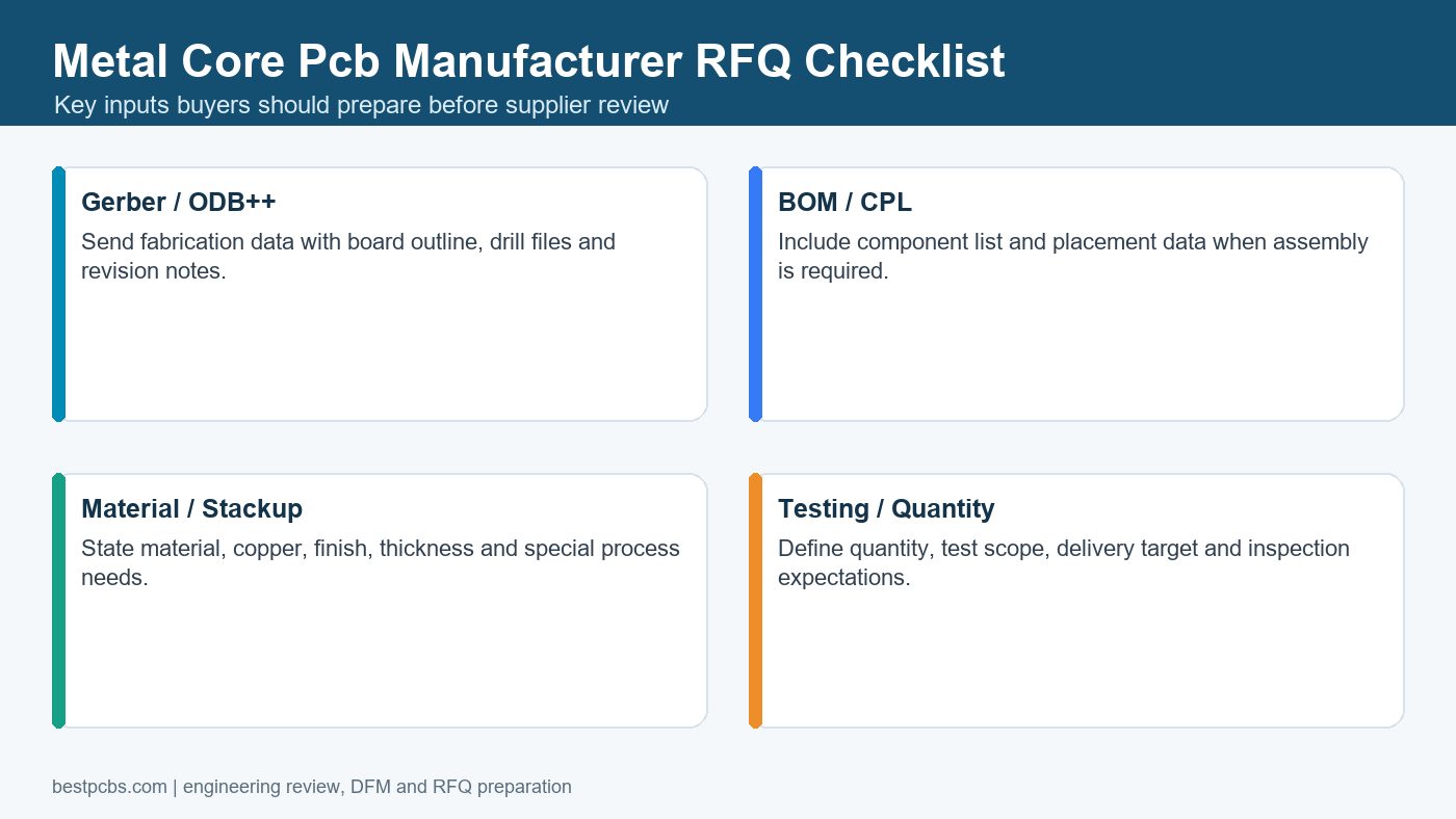
What Should You Include in a Metal Core PCB RFQ?

A complete RFQ reduces both price padding and schedule surprises. Send the same controlled package to every supplier:

  • Gerber or ODB++, drill files and revision-controlled fabrication drawing;
  • metal type and alloy, dielectric, finished copper and total thickness;
  • required thermal and electrical-isolation performance;
  • outline, slots, holes, countersinks, flatness, burr and V-score limits;
  • surface finish, solder mask, legend, panelisation and breakaway method;
  • electrical, isolation, dimensional and traceability deliverables;
  • prototype, pilot and repeat quantities, plus annual demand;
  • requested factory dispatch date, delivery address and Incoterm;
  • BOM, approved alternates, CPL, assembly drawing and test specification when PCBA is required.

Require the quotation to list deviations and exclusions beside the price. If the supplier proposes a different dielectric, omits a test or starts lead time only after a later approval, you should see that before comparing totals.

Metal Core PCB manufacturers in Spain, quality evidence and RFQ documents checked before ordering

FAQs About Metal Core PCB Manufacturers in Spain

Q1: Which Spanish supplier publishes a lead time for aluminium IMS?

A1: Fast PCB states 5 working days for short series and 10 working days for large series. CIPSA publishes a broader PCB prototype service of 24 hours to 5 days, but the requested IMS construction should be confirmed for that service.

Q2: Which companies publish copper IMS capability?

A2: CIRLAN and Maxwell Atlantic list copper as well as aluminium IMS. The quote should still identify the copper base, dielectric, factory and process limits for the part.

Q3: Which supplier publishes double-sided or PTH IMS structures?

A3: CIPSA publishes aluminium IMS options that include double-sided and PTH constructions. Ask for the current capability revision and the isolation method around plated features.

Q4: How should I compare metal core PCB prices?

A4: Compare the same material, quantity, tooling, tests, reports, packing, freight and delivery term. Separate bare-board and PCBA costs so missing work does not make one quote look artificially low.

Q5: What quality records should I request?

A5: Typical records include material identity, electrical-test results, isolation-test results, dimensional inspection, lot traceability and any agreed first-article report. Put required documents in the purchase order.

Q6: Does a short fabrication lead time include delivery to Spain?

A6: Usually not unless the quotation says so. Ask for the clock start, fabrication days, dispatch date, freight method and expected arrival date.

Q7: Can one supplier handle both metal-core PCB and assembly?

A7: Some overseas suppliers, including EBest Circuit, offer metal-core PCB fabrication, component sourcing, PCBA and testing together. The Spanish suppliers reviewed here mainly present bare PCB manufacturing services.

Q8: What files are needed for an accurate quotation?

A8: Send Gerber or ODB++, drills, stackup, fabrication drawing, thermal and isolation requirements, quantity and delivery target. Add BOM, CPL, assembly drawing and test instructions for PCBA.

Conclusion

The best supplier depends on the exact structure and delivery model. CIRLAN publishes detailed single-sided aluminium and copper IMS limits. Fast PCB provides the clearest stated series lead times for single-sided aluminium. Maxwell Atlantic offers broad in-house PCB processing and traceability. CIPSA publishes aluminium IMS structures that include double-sided and PTH options.

Compare quality evidence, total delivered cost, clock start, dispatch date and service scope before choosing. If you need a combined metal-core PCB and PCBA route for delivery to Spain, send Gerber or ODB++, stackup, quantities, BOM, CPL, assembly drawing, test requirements and target arrival date to sales@bestpcbs.com. EBest Circuit will provide a free DFM review and a project-specific quotation.

You may also like

Top Robotics 3D Vision Illuminator PCB Manufacturers in Germany
Thursday, August 27th, 2026

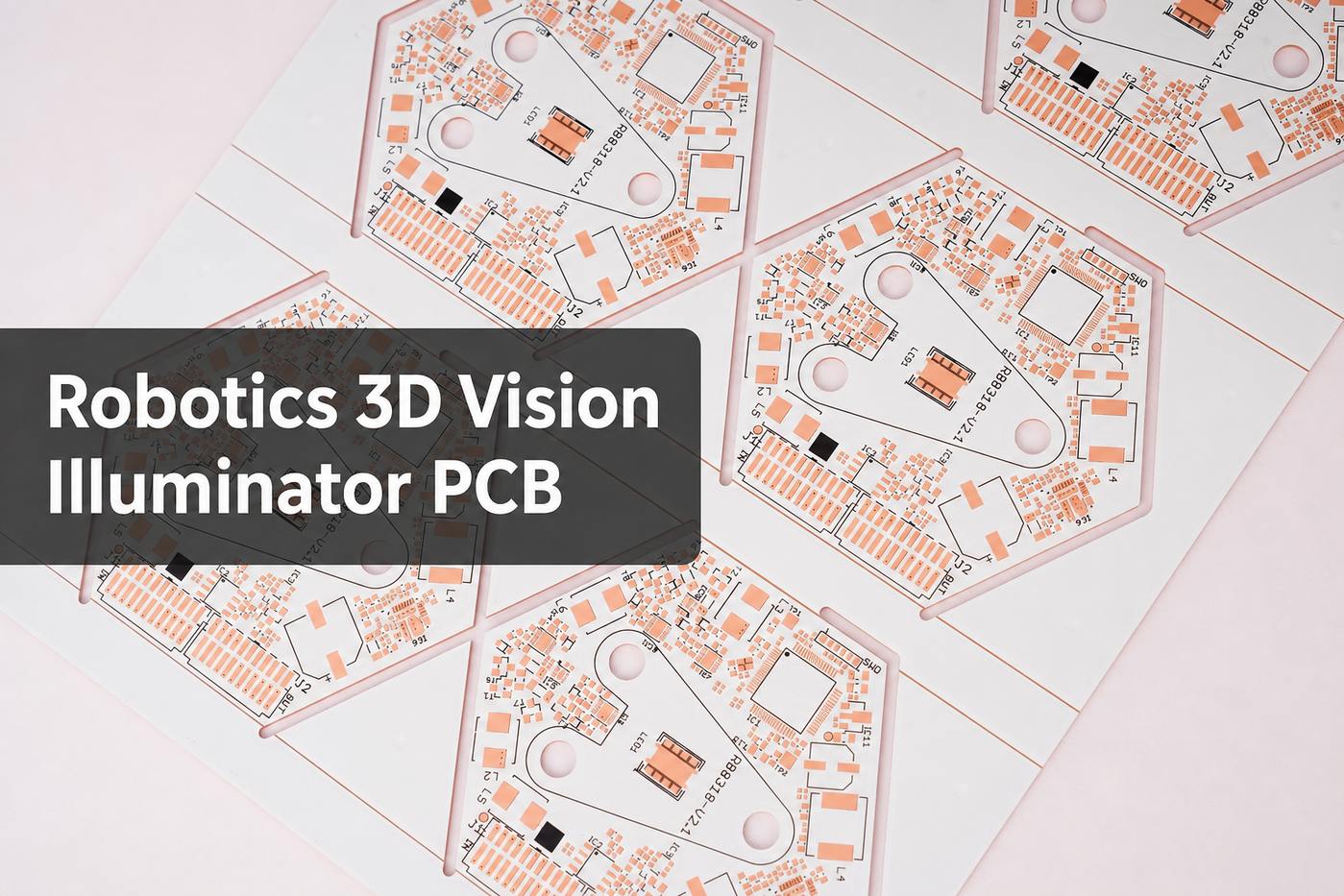
Top robotics 3D vision illuminator PCB manufacturers in Germany support lighting hardware that helps cameras capture stable depth data on reflective, dark, textured, or fast-moving objects. Choosing a supplier is not simply a matter of finding a company that can produce an aluminum PCB: the board must carry the LED load, remove heat, preserve optical consistency, fit the mechanical assembly, and arrive in time for camera and robot validation.

This guide helps German buyers assess manufacturers, prices, lead times, thermal capabilities, and sourcing routes for an illuminator PCB project. Buyers who also need a China manufacturing option can work with EBest Circuit, founded in 2006 and supported by 160 employees, more than 20 years of PCB and PCBA experience, 1,800+ customers across 40 countries, and a reported 97% on-time delivery rate. Its service combines PCB fabrication, component sourcing, PCBA, and testing. Send your Gerber files, BOM, target quantity, and required delivery date to sales@bestpcbs.com for an initial engineering review.

robotics 3D vision illuminator PCB

What Is a Robotics 3D Vision Illuminator PCB?

A 3D vision illuminator PCB is the circuit board that supports and drives the light source used by a robotic vision system. Depending on the sensing method, the illuminator may project infrared flood light, a structured pattern, a line, or synchronized pulses. The camera records the reflected light so that the vision system can calculate depth, locate parts, inspect surfaces, or guide a robot.

The PCB may look simple because LEDs dominate the visible side of the assembly, but its performance affects the complete optical system. Uneven LED current can create inconsistent brightness. Poor heat spreading can shift wavelength, reduce light output, shorten LED life, or distort calibration. Mechanical error can move the emitting surface away from the intended optical axis.

A buyer should therefore define the illuminator as an electro-optical assembly rather than as a generic LED board. Important inputs include:

  • illumination wavelength and optical power;
  • continuous, strobed, or pulsed operating mode;
  • LED quantity, package, current, and forward voltage;
  • required thermal resistance and maximum junction temperature;
  • board outline, mounting holes, connector position, and height restrictions;
  • driver topology, synchronization signals, and protection circuits;
  • camera distance, field of view, enclosure, lens, diffuser, or projector interface;
  • operating temperature, vibration, contamination, and service-life targets.

MCPCB is often suitable when the main challenge is removing heat from a compact LED array. A more complex illuminator may instead need a multilayer FR-4 board, a hybrid construction, or separate LED and control boards. The correct choice depends on the thermal path, signal requirements, component density, and mechanical design.

robotics 3D vision illuminator PCB

Top 3D Vision Illuminator PCB Manufacturers in Germany

The following companies are worth evaluating for thermal, high-reliability, prototype, or advanced PCB requirements in Germany. Their available services fit parts of an illuminator PCB project, but buyers should still confirm the MCPCB construction, PCBA scope, optical testing, available capacity, and production location for each quotation.

CONTAG AG, Berlin: CONTAG manufactures IMS and metal-core PCBs for LED, industrial, automotive, energy, and other thermally demanding applications. It also offers multilayer, HDI-SBU, high-frequency, flex, and rigid-flex boards. It is a strong candidate when an illuminator requires thermal engineering support, a fast German prototype, or a hybrid solution rather than a basic one-layer aluminum board.

Unimicron Germany GmbH, Geldern: Unimicron Germany offers multilayer boards up to 24 layers, HDI, high-frequency technology, metal-inlay solutions, IMS/heatsink technology, and other heat-management options. The company serves industrial and robotics applications, making it relevant when an illuminator combines power, control, communication, and thermal functions.

Becker & Müller Schaltungsdruck GmbH, Steinach: Becker & Müller provides in-house German production for prototypes and small batches and keeps IMS, FR-4, high-Tg, HF, and flex materials in stock. Its express service covers one- and two-sided boards, multilayers, and rigid-flex products. Buyers should ask which delivery option applies to the selected IMS material and stack-up.

Hotoprint Elektronik: Hotoprint manufactures PCBs in Germany, including multilayers up to 12 layers, flexible, rigid-flex, semiflex, and aluminum boards. Prototype and express services can begin from three working days, although the actual delivery date depends on the final MCPCB specification.

Leiton GmbH, Berlin: Leiton offers aluminum and copper IMS boards, German prototype production, an online calculator, and custom quotation support. Its Copper-IMS guide lists different lead-time options by layer count and shows which constructions require a direct enquiry.

This shortlist should begin a technical comparison, not end it. Some German companies focus mainly on bare PCBs, while a robotics buyer may need component sourcing, LED bin management, SMT assembly, programming, and functional testing. Ask each supplier to state exactly which operations are included and where they will be performed.

3D Vision Illuminator PCB Prices in Germany: What Buyers Should Compare

There is no reliable standard market price for a custom 3D vision illuminator PCB. Two boards with the same outline can have very different costs because price depends on material, panel utilization, copper weight, thermal dielectric, layer count, surface finish, tolerances, testing, quantity, and delivery speed.

For MCPCB prototypes, the main price drivers normally include:

  • aluminum versus copper base;
  • standard versus high-performance thermal dielectric;
  • one-layer, two-layer, or multilayer IMS construction;
  • board thickness and copper weight;
  • routed outline, slots, countersinks, or tight mechanical tolerances;
  • white solder mask, special marking, ENIG, or another nonstandard finish;
  • electrical test, documentation, and expedited manufacturing;
  • assembly quantity, LED package, placement density, and test coverage.

The lowest bare-board price is not always the lowest project cost. A cheaper board can become expensive if it needs a separate assembler, additional incoming inspection, repeated engineering communication, or rework after thermal testing. Conversely, paying a German prototype premium may be justified when local engineering contact or a very short iteration loop prevents a delayed robot trial.

Request quotations with the same manufacturing package and commercial assumptions. Each RFQ should specify quantity, panelization responsibility, material, copper, surface finish, test scope, tooling, delivery term, destination, and whether freight and tax are included. If PCBA is required, compare the BOM price, approved component sources, alternates, setup charges, programming, functional testing, and packaging separately.

A practical comparison uses at least three totals: prototype cost, landed cost, and cost of the next production quantity. This prevents an attractive sample price from hiding an unsuitable scale-up model.

What Lead Times Do German Manufacturers Offer for 3D Vision Illuminator MCPCBs?

German manufacturers publish useful benchmarks, but buyers must distinguish manufacturing time from delivery to the project site. The clock may begin only after data approval, material confirmation, DFM closure, and order release.

Leiton’s Copper-IMS technology document dated May 26, 2025, provides the clearest layer-specific public reference:

Copper-IMS constructionOnline calculationStandard on explicit enquiry
1 layer12 working days5 working days
2 layersNot availableFrom 4 working days
4-6 layersNot availableFrom 5 working days

These are Leiton’s manufacturing options for Copper-IMS boards. They are not universal German market lead times and do not automatically include assembly or shipping.

Eurocircuits lists five working days for bare boards and ten working days for assembled boards in its one-layer aluminum IMS pool. Because its PCB and assembly services are handled by factories in Germany and Hungary, buyers who require production specifically in Germany should confirm the assigned plant.

For project planning, separate the schedule into five parts:

  1. DFM review and clarification;
  2. special-material or component procurement;
  3. bare-board fabrication;
  4. assembly, programming, and functional testing;
  5. packing and transport to the German destination.

An advertised four- or five-day build does not help if a selected LED has a six-week procurement lead time. Send the complete BOM and approved-alternate policy early, and ask the supplier to state the ready-to-ship date rather than only the fabrication cycle.

Germany vs China for Robotics 3D Vision Illuminator PCB Manufacturing

Germany and China should not be compared through a single price or speed claim. The better choice depends on the development stage, specification stability, order quantity, communication needs, supply chain, and required manufacturing scope.

Buyer priorityGermanyChina
Local iterationStrong fitRemote review required
Integrated PCBASupplier-dependentCommonly available
Repeat-volume costQuote-dependentOften competitive
TransportShorter regional routeAdd freight and customs
Best useUrgent local prototypesIntegrated builds and scaling

A sensible sourcing strategy may use German manufacturing for an urgent local iteration and an approved China partner for integrated PCBA or repeat volume. Compare both options using the same material, stack-up, tolerances, surface finish, inspection scope, Incoterm, and delivery destination. If two sources will be used, approve the same golden sample before transfer.

Which MCPCB Process Capabilities Does EBest Circuit Offer for Robotics 3D Vision Illuminators?

For illuminator projects, EBest Circuit supports the following metal-base PCB production ranges:

ItemStandard capabilitySpecial capability
Thermal conductivity1-3 W/(m·K)3-8 W/(m·K), subject to material confirmation
Board constructionSingle-sided, double-sided, single-sided two-circuit-layer aluminum/copper baseSingle-sided four-layer, subject to review
Thermoelectric separationCopper-base PCBCopper-aluminum composite construction
Inner-layer copper0.5-3 oz4 oz or above, subject to review
Outer-layer copper1-3 ozAbove 3 oz, subject to review
Processing thickness0.8-3.0 mm4.0 or 5.0 mm by material order; bendable aluminum: 0.4-1.0 mm
Maximum aluminum-board size480 × 1180 mmSingle-sided aluminum: 1600 × 480 mm

Final capability depends on the complete files, material availability, and quantity.

robotics 3D vision illuminator PCB

What Lead Times Does EBest Circuit Offer for Robotics 3D Vision Illuminator PCBs?

For standard MCPCB prototypes below one square meter, buyers can use the following fabrication times as an initial planning reference. The confirmed schedule depends on the released specification and current capacity.

MCPCB layersNormal serviceFastest service
1 layer4 days24 hours
2 layers14 days168 hours
4 layers21 daysConfirm before ordering

These timings apply to standard MCPCB prototypes with a total order area below one square meter. The standard specification uses conventional aluminum material, 0.8-2.0 mm board thickness, 0.5 oz or 2 oz copper, lead-free HASL, white solder mask, black silkscreen, and nominal thermal conductivity of 0.8 W/(m·K).

High-conductivity materials, thermoelectric-separation copper-base PCBs, OSP, special copper weights, unusual thicknesses, tight tolerances, and nonstandard panel requirements need a project-specific schedule. Production timing begins after the manufacturing data, material choice, technical questions, and commercial terms are confirmed.

The table covers bare-board production only. Component purchasing, PCBA, functional testing, packing, international freight, customs clearance, and delivery within Germany must be added separately. If the project deadline is fixed, send the files and required arrival date to sales@bestpcbs.com so EBest Circuit can check current capacity and provide a realistic ready-to-ship schedule.

EBest Circuit Engineering Case: Building a Robotics 3D Vision Illuminator PCB

In a robotics 3D vision system, the illuminator must project repeatable light while the camera captures depth information. If heat builds up unevenly beneath the LED array, brightness can drift across the field of view and make optical calibration less stable. The PCB therefore acts as part of the lighting system, not just as a carrier for LEDs.

For one German illuminator project, EBest Circuit manufactured 180 pieces of a single-sided, two-circuit-layer thermoelectric-separation copper-base PCB. Its direct thermal path moved heat from the LED mounting area into the 1.5 mm copper base, while the isolated circuit layer carried power to the emitters. The specified 3 W/(m·K) material and 1 oz / 1 oz copper were selected to balance heat removal, current distribution, and the required 1.6 mm ±10% finished thickness.

The confirmed production specification was:

  • 1.5 mm copper base;
  • 1 oz / 1 oz copper;
  • thermal conductivity of 3 W/(m·K);
  • finished board thickness of 1.6 mm ±10%;
  • white solder mask and black silkscreen;
  • OSP surface finish;
  • delivery according to the customer’s panel drawing, with each individual board retaining its specified process rails.

White solder mask kept the LED side visually clean, black legend made polarity and assembly marks easy to identify, and OSP provided a flat surface for LED soldering. The boards were delivered in the customer’s released panel format with the required process rails, allowing the panels to enter LED assembly without repanelization.

Before production, the customer approved the final board configuration and panel format. The completed 180-piece lot was supplied with the requested COC and electrical test report. The German team therefore received one consistent board build for LED assembly and later camera-and-illuminator validation, without having to reconcile different thermal, mechanical, and panel specifications after delivery.

Why Choose EBest Circuit for 3D Vision Illuminator PCB Manufacturing?

EBest Circuit is a China-based PCB and PCBA manufacturing partner serving German and international buyers. Founded in 2006, the company has more than 20 years of industry experience, 160 employees, 1,800+ customers across 40 countries, and a reported 97% on-time delivery rate. It is most relevant when the project needs more than a bare-board price.

Technical support around the buyer: One sales contact is supported by three technical team members. DFM review, BOM optimization, and process-fit suggestions are available from engineers with long PCB and PCBA experience.

One project scope from board to test: PCB fabrication, component sourcing, PCBA, and customer-defined testing can be coordinated together, reducing handoffs between unrelated suppliers.

Prototype and low-volume support: Engineering samples and small batches help teams verify thermal behavior, mechanical fit, assembly, and optical performance before scaling.

Factory and supply-chain coverage: In-house PCB and PCBA resources are supported by more than 1,000 supply-chain partners, helping coordinate materials, components, quality controls, and delivery.

Traceability and quality systems: The digital workshop can trace material and product batches, production cycles, and progress. Available quality certifications include ISO 9001, ISO 13485, IATF 16949, and AS9100D.

A German manufacturer may still be preferable when physical production in Germany or immediate local iteration is mandatory. EBest Circuit is a stronger candidate when the buyer values integrated China sourcing, technical support, coordinated PCBA, traceability, and a route from prototypes to repeat production.

What Should You Send EBest Circuit for a 3D Vision Illuminator PCB Quote?

A first quotation does not need a perfect document package. To let EBest Circuit understand the project and identify missing information, start with five essentials:

  • your Gerber or ODB++ data, plus the board outline;
  • the LED or PCBA BOM if assembly is required;
  • prototype and expected production quantities;
  • known thermal targets, such as base material, conductivity, copper weight, or heatsink interface;
  • the German delivery location and the date the boards or assemblies are needed.

If your files are not complete yet, that is fine. Send what you have, and the engineering team will identify the few details needed next to evaluate price, manufacturability, thermal performance, and lead time. You do not need to prepare the full production package before requesting an initial review.

Email the available files to sales@bestpcbs.com and state that the request is for a robotics 3D vision illuminator PCB. EBest Circuit will review the current design, explain any information still needed, and prepare the quotation around your actual development stage.

FAQs About Robotics 3D Vision Illuminator PCB

Should a 3D vision illuminator use an aluminum or copper-base PCB?

Aluminum MCPCB is often suitable for cost-controlled LED heat spreading. Copper-base and thermoelectric-separation constructions can provide a more direct thermal path for higher heat density or tighter thermal targets. The right choice depends on LED power, pulse conditions, dielectric performance, mechanical structure, and the heatsink interface.

Can German manufacturers provide fast MCPCB prototypes?

Yes. Some German suppliers offer express or short prototype services. Leiton lists a five-working-day option for a one-layer Copper-IMS construction by direct enquiry, while more complex constructions require confirmation. Always check when the production clock begins and whether assembly and transport are included.

What should buyers compare besides the quoted PCB price?

Compare the metal base, dielectric, thermal conductivity, copper weight, board thickness, surface finish, tolerances, electrical test, documentation, tooling, panel delivery format, freight, and tax. For PCBA, also compare component sources, assembly setup, programming, functional testing, and approved alternatives.

Does EBest Circuit manufacture thermoelectric-separation copper-base PCBs?

Yes. EBest Circuit manufactures thermoelectric-separation copper-base PCBs. One completed German customer order used a single-sided, two-circuit-layer construction with a 1.5 mm copper base, 1 oz / 1 oz copper, 3 W/(m·K) thermal conductivity, OSP, and a finished thickness of 1.6 mm ±10%.

How can a German buyer reduce risk when sourcing an illuminator PCB from China?

Release a complete manufacturing package, approve the production data before fabrication, define acceptable materials and substitutions, agree on inspection and test reports, confirm the shipping term, and approve the pilot or golden sample before repeat production. These controls make the comparison more reliable than selecting a supplier by unit price alone.

Have a robotics 3D vision illuminator PCB ready for review? Email the available files, quantity, thermal requirements, and German delivery target to sales@bestpcbs.com. EBest Circuit will check the design, clarify the key manufacturing decisions, and respond with a quotation and project-specific schedule.

You may also like

Metal Core PCB Manufacturer for Heat-Critical Electronics
Saturday, July 18th, 2026
Metal core PCB manufacturer for aluminum and copper core circuit board fabrication

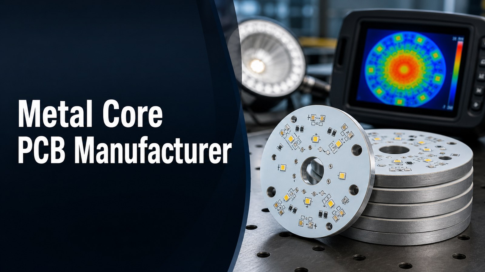
A metal core PCB manufacturer should help you control base material, dielectric performance, copper thickness, heat flow, DFM risk, assembly fit, testing scope and quote details before fabrication starts. Metal core PCB projects are usually chosen because heat cannot be treated as a secondary issue. If the board supports LEDs, power modules, motor controls, converters, industrial electronics or compact thermal assemblies, the manufacturing review must connect the circuit design with the real heat path.

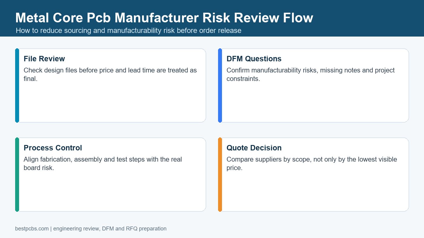
EBest Circuit supports metal core PCB buyers with metal core PCB manufacturing capabilities, file review, MCPCB material discussion, DFM feedback, optional PCBA coordination and RFQ planning. Send Gerber or ODB++, stackup notes, drawings, quantity, copper, surface finish, thermal requirements and assembly files early so the quote can be reviewed as a heat-critical build instead of a generic circuit board.

What Should a Metal Core PCB Manufacturer Help You Control?

A metal core PCB manufacturer should help control the thermal path, manufacturability and quotation scope of the board, not only the bare PCB price. A metal core PCB places an aluminum, copper or other metal base under the circuit structure so heat can move away from hot components more efficiently than on a normal FR4-only board.

The buyer’s main decision is not simply whether the board is called MCPCB, IMS PCB, aluminum PCB or metal-backed PCB. The practical questions are: which metal base is suitable, what dielectric is required, how much copper is needed, whether the stackup can be fabricated, how the board will be assembled, and how the finished build will be tested.

Is your metal core PCB quote risky because the heat path is not fully defined?

Metal core PCB projects often lose time before the first order because the RFQ package does not make the manufacturing risk visible enough:

  • The drawing names aluminum or copper core, but the dielectric, thermal conductivity target or final board thickness is not clear.
  • LED or power components create concentrated heat, yet the PCB files do not show how the heat should move through the board and mounting structure.
  • Copper thickness, hole size, line/space, solder mask bridge or surface finish expectations are copied from a standard PCB quote without MCPCB review.
  • The buyer asks for fast pricing, but the supplier cannot explain which values are standard, which need material confirmation and which need engineering review.
  • Assembly, test access and thermal inspection are discussed after fabrication, when layout and panel decisions are already harder to change.

Where Metal Core PCB Buyers Usually Lose Time Before Quotation

Metal core PCB buyers usually lose time when the supplier cannot separate standard manufacturing items from project-dependent thermal and material decisions. A fast quote is useful only when the manufacturing assumptions are correct. Otherwise, the first price can hide dielectric changes, copper changes, tooling review, thermal testing needs or assembly constraints.

For many teams, the first slowdown happens because the files describe the circuit, but not the thermal target. The next slowdown comes when the PCB quote and PCBA quote are handled separately. If the board will carry high-power LEDs or power devices, the bare board, mounting plan, soldering process and final test method should be reviewed together.

EBest Circuit helps buyers make metal core PCB risk visible before fabrication:

  • We review Gerber or ODB++ files together with stackup notes, base metal, dielectric, copper, surface finish, board thickness and drawing requirements.
  • We help identify whether aluminum, copper or stainless steel base material is a better starting point for the application and quote target.
  • We connect MCPCB fabrication review with PCBA support when BOM, CPL, LED orientation, soldering and test access affect the manufacturing result.
  • We keep special values as review items instead of turning them into unsupported promises when material sourcing or factory routing must be confirmed.
  • We help buyers compare quote scope, not only price, so the chosen supplier can support prototype, low-volume and repeat builds more predictably.

How EBest Circuit Reviews Metal Core PCB Projects Before Fabrication

EBest Circuit reviews metal core PCB projects by checking the thermal structure and manufacturing route before the buyer commits to fabrication. Our review starts with the file package, then checks base material, dielectric, copper, line/space, holes, solder mask, surface finish, routing, assembly files and test expectations.

This matters because metal core boards can look simple from the top copper layer, while the manufacturing risk sits inside the base material, insulation layer and heat-transfer path. When a value depends on the original files, material availability or special process route, we confirm it as part of the project review instead of writing it as a blanket claim.

Is a Metal Core PCB the Right Fit for Your Board?

A metal core PCB is a good fit when the board must move heat away from components more efficiently than a standard FR4 board can support. Common use cases include LED lighting, power supplies, automotive lighting modules, motor drives, industrial controls, converters, battery systems, RF power devices and compact electronics with concentrated heat sources.

Project Situation Why Metal Core Helps RFQ Question to Ask
High-power LED board Moves heat away from LED packages and solder joints What dielectric and base metal should support the thermal target?
Power electronics module Improves heat spreading under switching or power devices Does copper thickness, finish and assembly route match the load?
Compact thermal design Reduces dependence on board area alone for heat control How will the PCB connect to enclosure, heat sink or mounting surface?
Prototype moving to production Creates a clearer thermal manufacturing baseline Which values are standard and which need production confirmation?

Metal Core PCB Materials: Aluminum, Copper and Stainless Steel

Metal core PCB material selection should match the heat path, mechanical needs, cost target and fabrication route. EBest Circuit’s verified MCPCB capability source lists aluminum, copper and stainless steel as base material options. Aluminum is common for many LED and industrial thermal boards. Copper can be considered when higher heat spreading is required. Stainless steel is more application-specific and should be reviewed against the actual design.

Material naming alone is not enough for a good quote. Include the base metal, base material thickness, final board thickness, dielectric target, copper thickness, surface finish and mechanical drawing when you send the RFQ. If you are not sure which metal base is best, send the use case and thermal concern so the quote can start from a realistic structure.

Layer Count, Thickness, Copper and Line/Space Capability

Metal core PCB capability should be checked against the actual stackup because layer count, copper and thickness can change the manufacturing path. EBest Circuit’s verified MCPCB capability sheet lists 1-10 layers, 0.6 mm minimum board thickness, 4.0 mm maximum board thickness, 0.5 oz to 10 oz copper, 4/4 mil line/space, 8 mil minimum solder mask bridge and 10 mil minimum hole diameter.

Capability Area Verified Reference Buyer Note
Base materials Aluminum, copper, stainless steel Confirm against heat, cost and mechanical requirements
Layers 1-10 layers Send stackup for multilayer MCPCB review
Board thickness 0.6 mm to 4.0 mm in MCPCB sheet Some thicker material routes require confirmation
Copper thickness 0.5 oz to 10 oz in MCPCB sheet Heavy copper and fine features should be reviewed together
Line/space 4/4 mil (0.10/0.10 mm) Actual approval depends on copper, layout and process route
Surface treatment ENIG, ENEPIG, OSP, lead-free HASL Choose by soldering, shelf life and assembly needs

Dielectric and Thermal Conductivity Choices

The dielectric layer is one of the most important MCPCB quote decisions because it separates the circuit from the metal base while controlling heat transfer. EBest Circuit’s verified MCPCB capability sheet lists thermal conductivity examples of 1 W, 1.5 W, 2 W and 3 W. Higher thermal-conductivity material routes can be possible in some cases, but they require material and project confirmation.

For buyers, the best question is not “what is the highest number you can quote?” The better question is whether the dielectric, copper, base metal, soldering process and final mechanical assembly can meet the product’s thermal need at a controlled cost. A 3 W material may not automatically solve a poor heat path, and a lower thermal-conductivity material may still work when the layout, mounting and heat sink are well designed.

Metal core PCB stackup showing copper circuit dielectric metal core heat flow DFM review and testing

Metal Core PCB Manufacturing Process

The metal core PCB manufacturing process should be planned around stackup, insulation, copper patterning, drilling, surface finish, routing and inspection. A typical process starts with file intake and engineering review, then moves through material confirmation, imaging, etching, drilling, plating where applicable, solder mask, surface finish, profiling, electrical test and final inspection.

Metal core boards need special attention because the metal base affects drilling, routing, thermal behavior and handling. For double-sided, multilayer or thermally separated structures, the process route must be checked more carefully than a simple single-sided aluminum LED board.

Metal core PCB process overview from Best Technology.

DFM Checks Before MCPCB Fabrication

DFM review before MCPCB fabrication should check whether the design can be built, assembled, mounted and tested without avoidable thermal or manufacturing risk. Key review points include base metal, dielectric target, copper weight, line/space, hole size, solder mask bridge, surface finish, board outline, mounting holes, panelization, component heat sources and inspection method.

EBest Circuit’s process evidence shows why review language matters. Some values are standard; others depend on copper thickness, ordered material, special process route or factory confirmation. A good manufacturer should state this clearly before quoting so the buyer understands what is firm and what needs engineering confirmation.

Metal Core PCB Assembly and PCBA Support

Metal core PCB assembly should be planned with the thermal board from the beginning because component placement, soldering and test access can affect the final result. High-power LEDs, power packages, connectors and thermal interface points should be reviewed together with BOM, CPL, assembly drawing, polarity, package size and test requirements.

If your project needs turnkey support, EBest Circuit can connect metal core PCB fabrication with PCBA manufacturing and prototype PCB assembly planning. This helps avoid a common problem: the bare board is quoted first, but the soldering and final test assumptions are discovered too late.

Testing and Quality Checks for Heat-Critical Boards

Testing for heat-critical metal core boards should confirm both electrical function and manufacturing consistency. Depending on the project, checks may include electrical test, visual inspection, dimensional inspection, solderability review, thermal inspection, assembly inspection and project-specific documentation.

For LED and power electronics, test planning should be realistic. Ask what is included in the PCB quote, what belongs to assembly inspection, and whether any thermal or functional test needs a special fixture. A quote that ignores testing can look cheaper but create risk later.

What Determines Metal Core PCB Cost?

Metal core PCB cost is driven by material, dielectric, copper, board size, thickness, layer count, surface finish, inspection and assembly scope. The cheapest quote is not always the lowest-cost build if it leaves out thermal review, PCBA planning or test requirements.

Cost Driver Why It Matters RFQ Control Point
Base material Aluminum, copper and stainless steel have different cost and use cases State the preferred base metal or describe the thermal requirement
Dielectric Thermal conductivity and insulation affect performance and material cost Provide target thermal conductivity or ask for review
Copper and geometry Heavy copper, fine spacing and small holes change fabrication risk Send finished copper, line/space and drill requirements
Surface finish Finish affects solderability, shelf life and assembly path Choose ENIG, OSP, ENEPIG or lead-free HASL based on assembly needs
PCBA and test Assembly and testing can change total project cost more than bare PCB price Send BOM, CPL, assembly drawing and test plan with the PCB RFQ

How to Compare Metal Core PCB Suppliers

Compare metal core PCB suppliers by engineering review depth, thermal manufacturing fit and quote scope, not only by online unit price. A useful supplier should explain which requirements are standard, which are project-dependent, and what must be confirmed before production.

Check Item What to Ask Why It Matters
Thermal review Can they review base metal, dielectric and heat path before quote? MCPCB success depends on thermal structure, not only copper traces
Capability clarity Do they separate standard capability from values needing confirmation? It prevents unsupported assumptions from entering the purchase order
PCBA support Can they review BOM, CPL, LED orientation and test access? Thermal PCB risk often continues into assembly
Testing scope What inspection and test items are included? Quotes are not comparable unless test scope is clear
Production planning Can they support prototype, low-volume and repeat builds? The first build should not create a dead end for production

RFQ Checklist for a Metal Core PCB Manufacturer

A complete metal core PCB RFQ package should let the manufacturer review the board as a thermal product from the first message. Send these items when available:

  • Gerber or ODB++ files.
  • Fabrication drawing and board outline.
  • Base material preference: aluminum, copper, stainless steel or open for review.
  • Dielectric target or thermal conductivity requirement.
  • Layer count, final thickness, copper thickness and surface finish.
  • Quantity for prototype, low-volume or production order.
  • BOM, CPL, assembly drawing and test plan for PCBA projects.
  • Heat sink, enclosure, mounting, screw hole or mechanical interface notes.
  • Inspection, documentation, packaging and target delivery requirements.

Why Put EBest Circuit on Your MCPCB Quote List?

EBest Circuit is worth adding early to your metal core PCB quote list because thermal PCB sourcing works best when manufacturing, DFM, PCBA and cost control are reviewed together. We directly serve overseas buyers who need responsive engineering communication, stable quality, practical cost control, PCBA coordination and clear production planning for non-sensitive industrial, communication, LED, medical electronics, consumer electronics and small-to-medium batch projects.

Our advantage is not just that we can quote an MCPCB. The stronger reason to include EBest Circuit is that we can help you check the board before the quote becomes a purchase mistake. If your current supplier only prices the Gerber files, send the same package to us and compare the review depth, questions, manufacturing route and total project scope. For related thermal board planning, you can also read our aluminum PCB manufacturer guide and prototype PCB manufacturing RFQ guide.

FAQ About Metal Core PCB Manufacturers

What is a metal core PCB manufacturer?

A metal core PCB manufacturer fabricates circuit boards that use a metal base such as aluminum, copper or stainless steel to improve heat transfer from components. The manufacturer should review base material, dielectric, copper, surface finish, DFM risk, assembly needs and testing before quotation.

Is a metal core PCB the same as an aluminum PCB?

An aluminum PCB is one common type of metal core PCB, but not every metal core PCB uses aluminum. Metal core boards can also use copper or stainless steel depending on the project. The correct choice depends on heat flow, mechanical needs, cost and manufacturing route.

What files are needed for a metal core PCB quote?

Send Gerber or ODB++, fabrication drawing, stackup notes, base metal preference, dielectric target, copper thickness, surface finish, quantity and delivery target. For assembly, also send BOM, CPL, assembly drawing and test requirements.

Does a higher thermal conductivity dielectric always make the board better?

No. Higher thermal conductivity can help, but the full heat path matters. Copper layout, base metal, dielectric thickness, mounting method, heat sink contact, component placement and assembly quality also affect thermal performance.

Can EBest Circuit support metal core PCB assembly?

Yes. EBest Circuit can connect metal core PCB fabrication with PCBA support when the project needs BOM review, CPL checking, SMT assembly, test planning and production coordination. Send the assembly files together with the PCB files for a more complete review.

Final Recommendation

Choose a metal core PCB manufacturer that reviews the thermal structure before quoting, not one that only returns the fastest unit price. For heat-critical electronics, the right quote must match the base material, dielectric, copper, surface finish, assembly plan and inspection scope.

If you are preparing a metal core PCB or MCPCB assembly project, send your Gerber or ODB++ files, stackup notes, fabrication drawing, BOM, CPL, quantity, base material preference, dielectric or thermal target, copper thickness, surface finish, testing requirements and target schedule to sales@bestpcbs.com. EBest Circuit will review the files and help you build a clearer metal core PCB manufacturing quotation path.

You may also like

LED PCB Manufacturer for Heat-Controlled Lighting Boards
Friday, July 17th, 2026
LED PCB manufacturer inspecting high power LED metal core circuit boards

An LED PCB manufacturer should help buyers control heat, assembly risk, material choice and RFQ assumptions before the board moves into prototype or production. For LED lighting and power electronics, the board is not only a carrier for components. It is part of the thermal path, mechanical mounting system and quality-control plan.

EBest Circuit supports LED PCB and MCPCB projects where buyers need DFM review, metal-core material confirmation, PCB fabrication, PCBA support, component sourcing and clear quote communication. A useful quote should review the LED package, current, substrate, copper, dielectric, heat sink interface, assembly files, test expectations and production quantity together.

Are heat, assembly and mounting risks clear before you approve the LED PCB quote?

Many LED PCB problems become visible only after samples are powered, mounted or exposed to real operating conditions. A low board price is not useful if the thermal path, LED orientation or mounting surface was never reviewed.

  • The quote does not confirm whether FR-4, aluminum core, copper core, ceramic or a direct thermal path structure fits the heat load.
  • The LED package and solder pad design are reviewed separately from the housing, heat sink or thermal interface material.
  • The BOM and CPL are sent late, so LED polarity, driver parts, connector direction and test points are not checked before assembly.
  • The board outline looks simple, but mounting holes, flatness, dielectric choice and surface finish create production or installation risk.
  • The buyer compares prices without knowing which inspection, illumination check, electrical test or thermal check is included.

EBest Circuit reviews LED PCB projects as heat-control and assembly projects, not only as bare boards.

  • We review Gerber or ODB++ files, stackup, substrate notes, copper, finish, outline, LED package, BOM, CPL and quantity together.
  • We check whether the heat path from LED package to board, metal core, thermal interface and housing is clearly defined.
  • We help buyers identify missing RFQ details such as power level, mounting method, test requirements, polarity notes and target production stage.
  • We can connect LED PCB fabrication with PCBA support, component sourcing, inspection and production planning.
  • We keep material and process claims tied to project review, so special thermal structures are not treated as generic standard boards.

How Should Buyers Choose an LED PCB Manufacturer?

A buyer should choose an LED PCB manufacturer by checking thermal review, substrate options, assembly support, inspection scope, cost assumptions and RFQ communication.

For LED projects, a supplier that only quotes from Gerber files may miss the conditions that decide product reliability. The LED package, current, board material, copper, dielectric layer, heat sink interface, mounting pressure and enclosure design all affect how the finished board behaves.

The strongest supplier fit is not always the nearest or the lowest line item. It is the supplier that can review board construction, assembly data and production risk before tooling or mass production starts.

LED PCB Manufacturing Capabilities Buyers Should Confirm

LED PCB buyers should confirm metal-core material, layer count, board thickness, copper weight, thermal conductivity, trace/space, hole size and surface finish before approving a manufacturer.

Capability Area What to Confirm EBest Circuit Evidence Basis
Base material Aluminum, copper, stainless steel or another project-specific route MCPCB capability sheet lists Aluminum / Copper / Stainless steel
Thermal conductivity Dielectric thermal class and heat path expectation Sheet lists 1 W / 1.5 W / 2.0 W / 3.0 W entries
Layer count Simple metal-core board or multilayer MCPCB structure Sheet lists 1-10 layers
Board thickness Mechanical fit and mounting requirement Sheet lists 0.6 mm minimum and 4.0 mm maximum board thickness
Copper and routing Current path, trace width and heat spreading Sheet lists 0.5 oz-10 oz conductor thickness and 4/4 mil line/space
Finish Solderability, storage and assembly process Sheet lists ENIG, ENEPIG, OSP and HASL (LF)

These values are useful screening points, not a replacement for file review. The final quote should still check the drawing, LED package, assembly method, acceptance criteria and quantity.

LED PCB Thermal Path: What the Board Must Move Away From the LED

The thermal path should move heat from the LED package through the solder pad, copper, dielectric, metal core, thermal interface and heat sink or housing.

LED PCB thermal path from LED package through solder pad copper dielectric metal core and heat sink

In a high-power LED board, heat does not disappear inside the PCB. It must be guided toward a larger heat-spreading or heat-dissipating structure. If any part of the path is weak, the LED may still light during a sample test but lose brightness stability, solder reliability or service life under real load.

That is why LED PCB quotation should ask for more than outline, copper and quantity. The buyer should share LED power, expected mounting method, heat sink contact, operating environment, test conditions and whether the board is part of a lighting fixture, driver module or power electronics assembly.

MCPCB Materials: Aluminum, Copper and Stainless Steel Options

MCPCB material choice should follow heat load, mechanical support, weight, cost target and production method.

Aluminum core is often considered for LED lighting because it can provide a practical balance of heat spreading, weight and cost. Copper core can be considered when the design needs stronger heat spreading or current handling, but the quote must reflect material and process requirements. Stainless steel may be relevant for specific mechanical or environmental needs, but it should not be assumed without project review.

EBest Circuit’s checked MCPCB capability sheet lists aluminum, copper and stainless steel base material options. The right choice still depends on the LED package, board size, thermal target, mechanical installation and quantity.

FR-4, Metal Core, Ceramic or Direct Thermal Path: Which Route Fits?

The correct LED PCB route depends on heat density, electrical isolation, mounting, cost and product reliability requirements.

FR-4 can be suitable for low-power indicators, control sections or LED boards where heat density is modest and the system has enough margin. Metal core PCB is often considered when the board must spread heat away from LEDs more effectively. Ceramic PCB or direct thermal path structures may be evaluated for more demanding thermal designs, compact modules or high-power applications.

EBest Circuit has relevant internal-link paths for metal core PCB, direct thermal path board structures and ceramic PCB. The article does not claim one route is always best because the final choice depends on project files and operating conditions.

Copper Weight, Dielectric, Board Thickness and Surface Finish Choices

Copper weight, dielectric performance, board thickness and surface finish affect both thermal behavior and manufacturability.

Higher copper can support current and heat spreading, but it also changes etching, spacing and cost. Dielectric selection affects heat transfer and electrical isolation. Board thickness affects mechanical mounting, flatness and compatibility with the final housing. Surface finish affects solderability, storage and assembly planning.

The checked MCPCB sheet lists conductor thickness from 0.5 oz to 10 oz, board thickness from 0.6 mm to 4.0 mm, and surface treatments including ENIG, ENEPIG, OSP and HASL (LF). These should be treated as quote-review ranges because the final build depends on the drawing, stackup and process route.

LED Package, Polarity, Driver and Connector Assembly Checks

LED PCB assembly should verify LED polarity, package orientation, driver components, connectors, soldering access and test points before production.

A bare LED board can be fabricated correctly and still fail as an assembled product if LED polarity is unclear, the CPL is wrong, driver components are substituted without review, or connectors face the wrong direction. For PCBA work, the manufacturer should review Gerber, BOM, CPL and assembly drawings as one package.

For projects that need assembly, EBest Circuit can connect PCB fabrication with PCBA and PCB assembly support and component sourcing. That is important when LED binning, driver availability, approved alternates or connector lead time affects the final build.

DFM Review for LED PCB Manufacturing

DFM review should check whether the LED board can be fabricated, assembled, mounted, inspected and tested without avoidable risk.

Useful DFM checks include LED pad design, solder mask clearance, copper balance, thermal pad geometry, mounting holes, panelization, board outline, fiducials, silkscreen polarity marks, connector location, heat sink interface and test point access. If the board is metal core, the review should also consider mechanical processing and isolation requirements.

Buyers should treat DFM as part of supplier selection. A fast quote that ignores heat path and assembly data can become expensive after sample failure, fixture changes, rework or delayed production approval.

Testing and Inspection for LED PCB Projects

LED PCB testing should confirm electrical function, assembly correctness, visual quality and project-specific thermal or illumination requirements.

Common checks can include visual inspection, AOI, polarity checks, continuity, electrical test, solder joint review, connector inspection, sample illumination check and functional verification. For higher-risk products, the buyer may also define thermal test conditions, aging expectations or fixture-based tests.

Do not assume all LED PCB manufacturers include the same test scope in the base quote. If the project needs illumination, burn-in, thermal observation or functional testing, write those requirements into the RFQ.

What Drives LED PCB Manufacturing Cost?

LED PCB manufacturing cost is mainly driven by substrate, copper, dielectric, layer count, board size, assembly scope, testing, quantity and special thermal requirements.

Cost Factor Why It Changes the Quote Buyer Action
Substrate FR-4, aluminum, copper, ceramic and special thermal structures use different material and process routes State the preferred route or ask for engineering review
Thermal target Heat path requirements can affect dielectric, copper, metal base and inspection scope Share LED power, mounting and operating conditions
Assembly LEDs, drivers, connectors, sourcing and testing add process scope Send BOM, CPL and assembly drawings with the RFQ
Finish and copper Surface finish and copper weight affect fabrication and soldering Confirm finish preference and current requirements early
Quantity and stage Prototype, pilot and production orders have different setup and validation needs Give both first-build and repeat-order expectations

The lowest quoted board price is not always the lowest project cost. If a quote excludes assembly, LED sourcing, test requirements or thermal review, the missing scope can reappear later as delay or rework.

Prototype, Pilot and Production Planning for LED Boards

LED PCB prototypes should be planned so the same design can move toward pilot and production without rebuilding the supplier assumptions from zero.

A prototype often proves fit, brightness, current path and early thermal behavior. A pilot build checks repeatability, assembly flow, test method, packaging and production handling. A production run needs stable material sourcing, inspection records, approved alternates and a clear quality plan.

Tell the manufacturer whether the order is only a one-time prototype or the first step toward repeat production. That helps the supplier review panelization, material availability, test scope and cost assumptions more realistically.

Supplier Evaluation Checklist for LED PCB Buyers

A strong LED PCB supplier should ask about thermal path, material route, assembly files, testing and production stage before final quote approval.

  • Can the supplier explain whether FR-4, MCPCB, ceramic or a direct thermal path board fits the heat load?
  • Can they review LED package data, power level, current path, mounting and heat sink interface?
  • Can they support metal-core fabrication and PCBA when the project needs assembly?
  • Can they check BOM, CPL, LED polarity, driver parts, connectors and test requirements?
  • Can they separate standard capability from project-dependent thermal structures?
  • Can they give a quote that states assumptions instead of hiding missing scope?
  • Can they support prototype, pilot and production planning without forcing the same process on every order?

RFQ File Checklist for LED PCB Manufacturing

A complete LED PCB RFQ should include fabrication files, LED and thermal requirements, assembly data, testing scope, quantity and target schedule.

  • Gerber or ODB++ files, drill files and board outline.
  • Stackup notes, substrate preference, copper weight, board thickness and surface finish.
  • LED package, power/current information, heat path notes and mounting method.
  • Mechanical drawing, heat sink interface, mounting holes and enclosure constraints if available.
  • BOM, CPL, assembly drawing, LED polarity notes, driver details and connector direction.
  • Inspection, illumination, electrical, functional or thermal test requirements.
  • Prototype quantity, pilot quantity, production forecast and target schedule.

If some details are still open, mark them clearly. A good manufacturer can help review open questions, but it cannot safely quote assumptions that are never stated.

FAQ About LED PCB Manufacturers

What is an LED PCB manufacturer?

An LED PCB manufacturer builds printed circuit boards used for LED lighting, display, driver and power electronics projects. A strong supplier reviews thermal path, substrate, copper, assembly, testing and RFQ files, not only bare board fabrication.

What type of PCB is best for LED lighting?

The best type depends on heat load, current, mounting and cost. FR-4 can fit low-power LED boards, while aluminum core, copper core, ceramic or direct thermal path structures may be considered when heat density is higher.

What files are needed for an LED PCB quote?

Send Gerber or ODB++ files, drill files, stackup, material notes, LED package information, BOM, CPL, assembly drawing, quantity, surface finish and testing requirements. Heat sink or mounting information is useful for thermal review.

Can EBest Circuit support LED PCB assembly?

Yes. EBest Circuit can review LED PCB fabrication together with BOM, CPL, component sourcing, assembly drawings, inspection and testing requirements when the project needs PCBA support.

Why do LED PCB quotes vary so much?

Quotes vary because substrate, copper, dielectric, board size, finish, assembly, test scope, quantity and thermal requirements can all change the real work. A useful comparison must include the same RFQ files and assumptions.

Send Your LED PCB RFQ

If you need an LED PCB manufacturer for prototype, pilot or production work, send your Gerber or ODB++ files, stackup, LED package details, power/current notes, BOM, CPL, assembly drawing, quantity, material preference, surface finish, test requirements and target schedule to sales@bestpcbs.com. EBest Circuit will review the heat path, MCPCB options, fabrication details, assembly scope and quote assumptions before your project moves into production.

You may also like

Aluminum PCB Manufacturing Guide
Wednesday, July 15th, 2026
Aluminum PCB manufacturing for metal core thermal circuit boards

Aluminum PCB manufacturing builds a metal core circuit board by combining a copper circuit layer, thermally conductive dielectric and aluminum base so heat can move away from power components more efficiently than on a standard FR-4 board. It is commonly used for LED modules, power electronics, motor controls, automotive lighting and other heat-sensitive electronics.

This guide explains how aluminum PCBs are made, what supplier comparison landscape show for the topic, how to compare materials and thermal requirements, and what to send when requesting a quote.

Aluminum PCB Manufacturing at a Glance

An aluminum PCB is a type of metal core PCB designed to move heat from the copper circuit layer through a dielectric layer into an aluminum base. Buyers should confirm the thermal path, dielectric, copper thickness, surface finish, soldering method and testing requirements before ordering.

Layer or decision What to confirm Why it matters
Copper circuit layer Trace width, copper weight and component pads Controls electrical performance and current capacity.
Thermal dielectric Insulation, thermal transfer and manufacturability Moves heat while maintaining electrical isolation.
Aluminum base Thickness, flatness, outline and mounting needs Affects mechanical support and heat spreading.
Assembly and test LEDs, power parts, soldering, inspection and thermal checks Determines whether the finished board can handle the real load.

Is Your Aluminum PCB Project Being Held Back by Thermal Design Uncertainty?

Aluminum PCB buyers need more than a metal base; they need review of dielectric layer, copper, heat path, finish and assembly plan.

Customer Pain Point Project Risk How bestpcbs Helps
Heat source and thermal path are not defined The board may not remove heat from LEDs or power components effectively bestpcbs asks for operating environment, heat source location and board structure before quoting.
Dielectric layer assumptions are unclear Thermal performance and manufacturing cost can shift after release bestpcbs reviews material, thickness, copper and finish requirements during RFQ review.
Assembly requirements are not tied to thermal design Component placement and soldering can affect reliability bestpcbs checks BOM, CPL and assembly notes together with the fabrication package.
Testing and inspection are left open The buyer may not know whether the board was checked against project needs bestpcbs confirms electrical and project-specific inspection requirements before shipment.

Aluminum PCB Buyer Priorities Before Production

Aluminum PCB manufacturing should be reviewed around heat transfer, dielectric layer, copper, solder mask, LED or power component placement, surface finish and assembly needs. Thermal performance depends on more than the metal base alone.

Before quoting, share heat source location, operating environment, board thickness, copper weight, surface finish, component data and testing expectations. This lets the supplier check whether the design is ready for prototype or production manufacturing.

Aluminum PCB vs Metal Core PCB

Aluminum PCB is the most common type of metal core PCB, but metal core PCB can also refer to other metal base constructions depending on the project. In most buyer conversations, aluminum PCB and MCPCB overlap because aluminum is widely used for thermal boards.

For broader supplier selection, compare this article with the metal core PCB manufacturer RFQ guide.

When Aluminum PCB Is the Right Choice

Aluminum PCB is a good fit when the board needs better heat transfer, mechanical stability and a direct thermal path for components such as LEDs, power ICs or switching devices. It is not automatically required for every board with heat, but it is often considered when FR-4 cannot move heat away fast enough.

  • LED lighting boards and high-brightness LED modules
  • Power conversion, drivers and current-control boards
  • Motor control and industrial power interfaces
  • Automotive lighting and thermal electronics modules
  • Heat-sensitive assemblies mounted to a chassis or heat sink

Aluminum PCB Manufacturing Process

The manufacturing process generally starts with material selection and circuit imaging, then moves through etching, drilling, solder mask, surface finish, profiling, inspection and packaging. The process must protect both electrical isolation and thermal performance.

  1. Review Gerber or ODB++ files, drawings, copper, finish and thermal notes.
  2. Select the aluminum base and thermally conductive dielectric according to the application.
  3. Create the copper circuit pattern through imaging and etching.
  4. Drill, route and profile holes, slots and board outlines.
  5. Apply solder mask, silkscreen and surface finish.
  6. Inspect dimensions, circuit quality, solderability and packaging condition.

Thermal Design Questions Buyers Should Answer

The supplier cannot judge thermal suitability from Gerber files alone; the buyer should describe the heat source, operating environment and mechanical heat path. This helps prevent a board from being quoted as a generic aluminum PCB when the real thermal risk is higher.

  • What components generate the most heat?
  • What is the expected current, power or temperature rise concern?
  • Will the aluminum base contact a heat sink, chassis or thermal interface material?
  • Are there mounting holes, flatness needs or insulation requirements?
  • Is the build a prototype, pilot run or production order?

Materials, Copper and Surface Finish

Material choices should match the electrical load, soldering process, thermal path and final operating environment. Aluminum base thickness, copper weight, dielectric behavior and surface finish can change both manufacturability and cost.

If the board also needs assembly, the soldering method and component package should be discussed early. For boards that require mounted LEDs, power parts or connectors, use the PCBA service path so fabrication and assembly are reviewed together.

DFM Checks Before Aluminum PCB Production

DFM review should confirm that thermal, electrical and mechanical requirements are all manufacturable before the quote is approved. Important checks include copper clearance, solder mask openings, mounting holes, board outline, slots, thermal pad geometry, component-to-edge distance and panelization.

For layout preparation, the PCB design and manufacturing DFM guide gives a useful framework before releasing files.

Testing and Quality Control

Quality control should verify the electrical circuit, visual condition, dimensions, solderability and any customer-defined thermal or assembly requirements. A basic board test does not replace application-level thermal validation, so buyer and supplier responsibilities should be separated clearly.

Check Purpose Buyer note
Electrical test Finds opens and shorts in the circuit Provide netlist or accepted test scope.
Dimensional inspection Confirms outline, mounting holes and mechanical fit Send drawing and critical tolerances.
Assembly inspection Checks solder joints, polarity and component placement Send BOM, CPL and assembly drawing.
Thermal validation Confirms heat performance in real use Define whether buyer or supplier performs this test.
aluminum pcb manufacturing RFQ checklist for supplier review
aluminum pcb manufacturing RFQ checklist for supplier review.
aluminum pcb manufacturing risk review flow before production
aluminum pcb manufacturing risk review flow before production.

What Determines Aluminum PCB Cost?

Aluminum PCB cost depends on board size, aluminum base, dielectric, copper weight, finish, drill and routing complexity, quantity, assembly and testing requirements. Thermal boards can look simple but still require careful quote assumptions.

For cost planning, compare the project with the custom PCB cost guide and list the thermal requirements instead of only asking for the cheapest aluminum PCB.

RFQ Checklist for Aluminum PCB Manufacturing

A complete RFQ should tell the supplier what the aluminum PCB must do thermally, electrically and mechanically. This prevents quote revisions after the supplier discovers missing thermal or assembly details.

  • Gerber or ODB++ files, drill files and board outline drawing.
  • Material, aluminum base thickness, copper weight, board thickness and surface finish.
  • Thermal load, heat sink or chassis contact notes if available.
  • Quantity, prototype or production stage, target lead time and shipment destination.
  • BOM, CPL, assembly drawing and polarity notes if assembly is required.
  • Electrical test, dimensional inspection, packaging and thermal validation expectations.

Frequently Asked Questions About Aluminum PCB Manufacturing

Is aluminum PCB the same as metal core PCB?

Aluminum PCB is a common type of metal core PCB. Metal core PCB is the broader category, while aluminum PCB specifically uses an aluminum base layer.

Why use aluminum PCB instead of FR-4?

Aluminum PCB is used when heat needs to move away from components more efficiently. Standard FR-4 may still be suitable for boards without strong thermal requirements.

Can aluminum PCB be assembled with LEDs and power components?

Yes, but the BOM, CPL, soldering process, polarity, thermal interface and inspection requirements should be reviewed before production.

What should I send for an aluminum PCB quote?

Send Gerber or ODB++, drill data, material and thermal notes, copper weight, finish, quantity and delivery target. For assembly, also send BOM, CPL and assembly drawings.

Final RFQ Recommendation

Before ordering aluminum PCB manufacturing, define the thermal path as clearly as the circuit pattern. The supplier needs to know whether the board is a simple metal core build, an LED thermal board, a power electronics board or an assembly-ready module.

For an aluminum PCB quote, send your Gerber or ODB++ files, drill data, BOM, CPL, assembly drawing, quantity, material expectations, copper weight, surface finish, thermal requirements, testing needs and target lead time to sales@bestpcbs.com. The Best Technology / bestpcbs team can review the files and confirm what needs project-specific checking before production.

You may also like

Metal Core PCB Manufacturer Selection Guide
Wednesday, July 15th, 2026
Metal core PCB manufacturer guide showing aluminum LED boards and thermal inspection

A metal core PCB manufacturer builds printed circuit boards that use an aluminum, copper or stainless steel base to move heat away from components more effectively than standard FR4 boards. Buyers usually search this keyword when they need MCPCB fabrication for LED lighting, power electronics, motor control, thermal modules or compact assemblies where heat cannot be ignored.

This guide explains how to compare metal core PCB manufacturers, what capability data to ask for, which files to prepare and how to avoid quote errors. It is based on the current supplier comparison landscape and verified Best Technology MCPCB capability data from the company process capability sheet.

Metal Core PCB Manufacturer at a Glance

A good metal core PCB manufacturer should be evaluated by thermal path, core material, dielectric, layer count, copper thickness, mechanical tolerance, surface finish, DFM review and assembly support. The lowest quote is not useful if the thermal requirement is misunderstood.

Decision area What to confirm Why it matters
Core material Aluminum, copper or stainless steel Controls heat spreading, weight, machining and cost.
Thermal conductivity Dielectric thermal performance and heat path Determines whether heat can leave LEDs or power devices.
Layer structure Single layer, double layer or multilayer MCPCB Changes routing freedom and manufacturing complexity.
Assembly scope BOM, CPL, polarity, thermal pads and inspection Many MCPCB projects fail at assembly details.

Is Your Metal Core PCB Project Being Limited by Thermal Assumptions?

Metal core PCB buyers need a supplier review that connects heat path, dielectric layer, copper, finish and assembly requirements.

Customer Pain Point Project Risk How bestpcbs Helps
Thermal path is not defined The board may not move heat away from LEDs or power devices as expected bestpcbs asks for heat source location, operating environment and board structure before confirming the build path.
Dielectric and copper choices are unclear Thermal behavior, cost and manufacturability can shift after quoting bestpcbs reviews material, copper, thickness and finish expectations during RFQ review.
Assembly needs are separated from board design Component placement and soldering constraints may affect thermal performance bestpcbs checks BOM, CPL and assembly notes together with fabrication files when PCBA is needed.
Testing expectations are not written down The buyer may not know which checks protect shipment quality bestpcbs confirms electrical and project-specific inspection requirements before production.
metal core pcb manufacturer RFQ checklist for supplier review
metal core pcb manufacturer RFQ checklist for supplier review.
metal core pcb manufacturer risk review flow before production
metal core pcb manufacturer risk review flow before production.

What Is the Metal Core of a PCB?

The metal core of a PCB is the heat-spreading base layer, usually aluminum or copper, placed under the circuit layer and dielectric to conduct heat away from high-power components. It is the reason MCPCBs are common in LED and power designs.

A basic metal core board includes a copper circuit layer, a thermally conductive dielectric and a metal base. Some designs use a direct thermal path structure such as 1 Layer SinkPAD Board when the heat path must be shorter than a conventional insulated metal substrate.

Metal Core PCB Buyer Priorities Before Supplier Selection

Metal core PCB buyers should confirm thermal path, dielectric selection, copper thickness, surface finish, assembly needs and testing before choosing a supplier. The lowest quote can become expensive if heat transfer or LED reliability requirements are unclear.

Share operating environment, heat source location, board thickness, copper weight, insulation expectations and assembly details so the supplier can review the project as a thermal product rather than a standard FR-4 board.

Metal Core PCB Capability Checklist

Best Technology capability data lists aluminum, copper and stainless steel base material options for MCPCB projects, with multiple base thicknesses, thermal conductivity levels and surface finishes. Use these figures as a quoting checklist, not as a substitute for project-specific engineering review.

Capability item Verified Best Technology data
Base materials Aluminum, copper and stainless steel
Base material thickness, excluding copper 0.30mm to 3.0mm listed options
Thermal conductivity 1W, 1.5W, 2.0W and 3.0W options
Layer count 1-10 layers
Board thickness 0.6mm to 4.0mm
Copper thickness 0.5oz to 10oz
Minimum line width/space 4/4mil, 0.10/0.10mm
Surface treatment ENIG, ENEPIG, OSP and lead-free HASL

Aluminum, Copper and Stainless Steel Core Options

Aluminum core boards are common for cost-effective heat spreading, copper core boards are used when stronger thermal performance is needed, and stainless steel may fit projects with mechanical or environmental constraints. The right base depends on heat, weight, machining and budget.

The Metal Core PCB product page is the primary internal capability page for MCPCB, IMS boards, copper core boards and aluminum core boards.

Thermal Conductivity and Heat Path Decisions

Thermal conductivity should be selected from the heat target, component power, board area, dielectric, metal base and final heat sink connection. Do not choose a thermal value only because it sounds higher.

For high-power LEDs or power modules, ask whether the heat must pass through the dielectric or whether a direct thermal path structure is more suitable. If routing needs more copper layers on one side, review the Double Layers MCPCB option.

Layer Count, Thickness, Copper and Feature Limits

Metal core PCB complexity is controlled by layer count, total thickness, copper thickness, minimum line width/space, hole requirements and board size. These features should be fixed before comparing quotes.

Best Technology’s MCPCB sheet lists 1-10 layers, 0.6mm to 4.0mm board thickness, 0.5oz to 10oz copper and 4/4mil minimum line width/space. These values help buyers decide whether the board belongs in standard MCPCB, multilayer MCPCB or a more specialized thermal board review.

Surface Finishes, Solder Mask and Mechanical Details

Surface finish, solder mask color, hole tolerance and outline tolerance affect assembly quality and mechanical fit, especially on LED boards and metal housings. They should appear in the RFQ rather than being left to default settings.

The verified MCPCB sheet lists ENIG, ENEPIG, OSP and lead-free HASL as surface treatments, plus solder mask oil options in white, black, green, blue, yellow and red. White solder mask is common for LED lighting designs, but it should still be specified.

LED, Power Electronics and Heat Sink Applications

Metal core PCBs are commonly used when components generate enough heat that FR4 would make the design less reliable or less compact. Typical applications include LED lighting, power converters, motor controls, automotive lighting, heat sink modules and high-current control boards.

For LED projects, thermal path, surface reflectivity, mounting holes and polarity markings should be checked together. For high-current power projects, copper weight, creepage, clearance and mechanical grounding should be reviewed before release.

DFM Review Before MCPCB Manufacturing

DFM review for MCPCB should check thermal pads, dielectric isolation, drilling, routing, board outline, metal exposure, solder mask bridge, copper weight and assembly clearance. A file that works for FR4 may not automatically be ready for metal core production.

Ask the manufacturer to review Gerber or ODB++ files, drill files, drawings and stackup notes before accepting the order. If the project has dense assembly, include the PCBA and PCB assembly service scope in the same conversation.

PCB Assembly and Component Sourcing for MCPCB

MCPCB assembly should be planned around thermal pads, LED polarity, component height, solder profile, heat-sensitive parts and inspection method. The bare board may be correct while the assembled board still fails if thermal and assembly details are separated.

Provide BOM, CPL, assembly drawing, polarity notes and any LED binning or approved substitution rules. If components are included, component sourcing support should be reviewed before the quote is finalized.

What Determines Metal Core PCB Cost?

Metal core PCB cost is driven by base material, thermal conductivity, layer count, copper thickness, board size, surface finish, machining, assembly scope, testing and lead time. A useful quote makes these assumptions visible.

Cost factor Why it matters Buyer action
Base metal Copper and special cores can cost more than standard aluminum. State the thermal reason for the base choice.
Thermal conductivity Higher thermal dielectric requirements can change material cost. Use thermal simulation or component data to justify the value.
Mechanical work Slots, countersinks, special holes and metal machining add process steps. Send clear mechanical drawings.
Assembly LED placement, polarity and thermal soldering add inspection needs. Include BOM, CPL and assembly notes in the first RFQ.

How to Compare Metal Core PCB Manufacturers

Compare metal core PCB manufacturers by verified capability, thermal engineering support, application fit, quote clarity and assembly readiness. A supplier that only repeats “MCPCB available” has not answered the real sourcing question.

  • Can the manufacturer explain aluminum versus copper core tradeoffs?
  • Do they ask for thermal conductivity and heat sink assumptions?
  • Can they support single-layer, double-layer or multilayer MCPCB if needed?
  • Do they review mechanical holes and board outline before quoting?
  • Can they support assembly and testing for LED or power boards?
  • Do they provide a clear RFQ path for prototype and repeat orders?

For broader supplier checks, the PCB assembly manufacturer RFQ checklist is useful when the MCPCB will be assembled rather than ordered as a bare board.

RFQ File Checklist for Metal Core PCB Projects

A complete MCPCB RFQ should describe the thermal requirement, not only the copper artwork. This is where many metal core PCB quotes become unclear.

  • Gerber or ODB++ files and drill files.
  • Layer count, base metal, dielectric and total thickness.
  • Thermal conductivity requirement and heat sink contact area.
  • Copper thickness, surface finish and solder mask color.
  • Mechanical drawing for holes, slots, cutouts and tolerances.
  • BOM, CPL and assembly drawing if PCBA is included.
  • Testing, inspection, quantity and target lead time.

Frequently Asked Questions About Metal Core PCB Sourcing

What is a metal core PCB?

A metal core PCB is a printed circuit board with a metal base, usually aluminum or copper, used to improve heat spreading from components such as LEDs and power devices.

Is aluminum or copper better for MCPCB?

Aluminum is common for cost-effective thermal boards, while copper is selected when stronger heat spreading is required. The best choice depends on thermal load, weight, machining and budget.

Can metal core PCB include assembly?

Yes. MCPCB projects can include assembly, but the RFQ should include BOM, CPL, polarity notes, thermal pad requirements and inspection criteria.

What should I ask a metal core PCB manufacturer?

Ask about base material, thermal conductivity, thickness, copper, layer count, surface finish, mechanical tolerance, DFM review, assembly support and testing.

Final RFQ Recommendation

Choose a metal core PCB manufacturer only after the thermal path, core material, dielectric, copper, surface finish, mechanical details and assembly scope are clear. MCPCB is a heat-management decision as much as a PCB fabrication decision.

For a metal core PCB quote, send Gerber or ODB++ files, drill files, stackup and base material notes, thermal conductivity target, board thickness, copper thickness, surface finish, solder mask color, quantity, BOM, CPL, assembly drawings, testing requirements and target lead time to sales@bestpcbs.com. Best Technology / bestpcbs can review the package and help confirm whether the project fits standard MCPCB, aluminum PCB, copper core PCB, SinkPAD, PCBA or another thermal-board structure.

You may also like

Custom Metal-Backed PCB Lead Times: Materials and Supplier Checks
Monday, July 13th, 2026
Metal-backed PCB lead time planning with aluminum core PCB samples and RFQ documents

Custom metal-backed PCB lead times depend on material availability, stackup complexity, copper or aluminum base selection, surface finish, routing profile, testing requirements and how complete the RFQ files are. A supplier can usually quote faster when the Gerber files, drill data, stackup, base metal requirement, thermal target, quantity, finish and assembly needs are clear before review. If any of those items are missing, the schedule often stalls before production even starts.

This guide is written for buyers and engineers comparing custom metal-backed PCB lead times between suppliers. It focuses on the practical checks that affect delivery risk for aluminum PCB, copper core PCB, MCPCB and direct thermal path boards, not generic promises about speed.

What affects custom metal-backed PCB lead times?

The biggest schedule drivers are material choice, thermal structure, fabrication process, assembly scope and review quality before release. Metal-backed boards are not always difficult, but they are less forgiving than a simple FR4 prototype because the base metal, dielectric layer and mechanical profile all affect thermal performance and manufacturability.

For a standard single-layer Metal Core PCB, the factory review usually starts with the aluminum or copper base, dielectric thermal conductivity, copper weight, solder mask, finish and outline method. For double-sided or multi-layer designs, the review becomes more detailed because plated holes, layer registration, insulation, flatness and heat path design must be checked together.

Lead time factorWhat the supplier checksWhy it can slow the schedule
Base metalAluminum, copper, iron alloy or direct thermal path structureNon-standard base thickness or copper base availability may need confirmation
Dielectric layerThermal conductivity, insulation strength and thicknessSpecial dielectric materials may require extra sourcing or DFM review
Copper weightTrace width, spacing, current load and etching controlHeavy copper changes etching, solder mask and inspection risk
Mechanical profileCNC routing, V-cut, milling, countersink or unusual shapeMetal substrates often need slower tool paths and tighter fixture planning
Assembly and testLED polarity, thermal pad contact, functional test and packagingPCBA adds component sourcing, SMT scheduling and quality checks

Which RFQ files should be ready before asking suppliers?

A complete RFQ package removes the most common waiting time: back-and-forth clarification. At minimum, prepare Gerber files, drill files, board drawing, stackup request, base material notes, copper weight, surface finish, solder mask color, quantity, target date and whether the order includes assembly.

Engineer reviewing metal-backed PCB samples, stackup drawing and production schedule before RFQ
Complete files help the supplier confirm material, stackup, routing and schedule before production release.
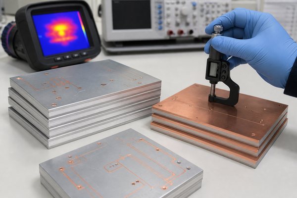
For boards with LEDs or power devices, include thermal assumptions instead of only sending the circuit image. The supplier needs to know whether the board is a general aluminum PCB, copper core PCB, SinkPAD Board, or another direct thermal path design. If the design needs a special heat path, the lead time should not be judged from a normal MCPCB quote.

  • Gerber and drill data with clear revision control.
  • Mechanical drawing with board thickness, outline tolerance and hole notes.
  • Stackup or construction requirement, including base metal and dielectric.
  • Copper weight, surface finish and solder mask requirement.
  • Assembly BOM, centroid file and polarity notes if PCBA is included.
  • Testing requirement, packaging method and any thermal validation request.

Which material choices change the schedule?

Material choices change lead time when they are outside the supplier’s normal stock, need tighter thermal control or require a different fabrication route. A basic aluminum substrate is usually easier to plan than a copper core board, a double-sided MCPCB or a multi-layer metal-backed build.

A double-sided MCPCB needs closer review than a single-sided board because the supplier must confirm insulation, drilling, plating, alignment and surface preparation through a metal base structure. High-current areas may also push the design toward heavier copper, larger spacing or local thermal relief. If the same design also needs SMT, conformal coating, box build or special packaging, the buyer should treat fabrication and assembly as one schedule instead of two separate dates.

When the material is the main risk, ask the supplier to confirm whether the base metal, dielectric and copper foil are stocked, reserved or still pending procurement. A fast quote is not the same thing as confirmed material availability.

How should suppliers review manufacturability before committing a date?

A reliable supplier should check the thermal structure, mechanical profile, copper design and test plan before promising a ship date. The best warning sign is not a long lead time; it is a very fast promise made before anyone has checked the metal substrate details.

For metal-backed PCB projects, DFM review should include conductor spacing, copper-to-edge distance, dielectric isolation, heat path, milling risk, solder mask coverage and finish compatibility. If assembly is included, the review should also include component availability through Component Sourcing, stencil design, polarity, thermal pad soldering and inspection method.

Ask the supplier to identify what is fixed and what is still conditional. A clear answer might say: material is available, outline needs CAM review, assembly components need two substitutes approved, and functional testing needs a fixture. That kind of detail is more useful than a one-line promise.

Where do testing and assembly fit into the lead time?

Testing and assembly should be scheduled before the order is released, not discovered after boards are fabricated. A bare board schedule only covers fabrication. A real project schedule may also include SMT, through-hole assembly, cleaning, AOI, electrical test, thermal contact checks, fixture setup and final packaging.

MCPCB production panels under probe testing before shipment
Electrical inspection, routing and final handling can affect the delivery date for metal-backed PCB panels.

If your order includes prototype PCB assembly, the supplier must align PCB fabrication, component arrival, SMT line time and quality checks. For production builds, test fixtures and packaging can matter just as much as board fabrication. Use the supplier’s PCB test equipment capability as a schedule discussion point, especially when the board drives LEDs, power modules, sensors or high-current loads.

Metal core PCB process footage can help buyers understand why material preparation, routing and inspection need schedule space.

Supplier checklist before placing the order

The safest order decision comes from confirming files, materials, DFM status, assembly scope and test requirements in writing. Use the checklist below before approving a custom metal-backed PCB lead time.

  1. Confirm the supplier has reviewed the latest Gerber, drill, drawing and stackup files.
  2. Ask whether the aluminum, copper or special dielectric material is in stock or needs procurement.
  3. Confirm the board type: standard MCPCB, copper core, double-sided MCPCB, SinkPAD or another thermal structure.
  4. Ask which process step is most likely to affect delivery: material, CAM, drilling, routing, finish, assembly or testing.
  5. Confirm whether component sourcing and substitutes are approved before SMT scheduling.
  6. Require a final delivery date after DFM review, not before the supplier has checked the files.
  7. Keep one controlled revision package so the quote, production order and inspection plan match.

For high-power or thermal products, also review related material guidance such as Metal Core PCB Material. Material choice is often where schedule, cost and reliability meet.

FAQ

How should buyers compare custom metal-backed PCB lead times between suppliers?

Compare suppliers after the same RFQ package has been reviewed. If one supplier quotes from a finished DFM review and another quotes from an email summary, the dates are not equal. Ask each supplier to state material availability, CAM status, assembly scope, testing needs and open questions.

Is an aluminum PCB always faster than a copper core PCB?

Not always, but a standard aluminum PCB is often easier to schedule when material is stocked and the design is simple. Copper core, direct thermal path and unusual mechanical profiles usually need more review because heat transfer, insulation and routing risks are higher.

What causes the most common RFQ delays?

Missing drawings, unclear base material, incomplete drill data, uncertain copper weight, unapproved component substitutes and vague testing requirements cause many delays. The supplier can quote faster when the buyer sends a controlled file set and answers technical questions before release.
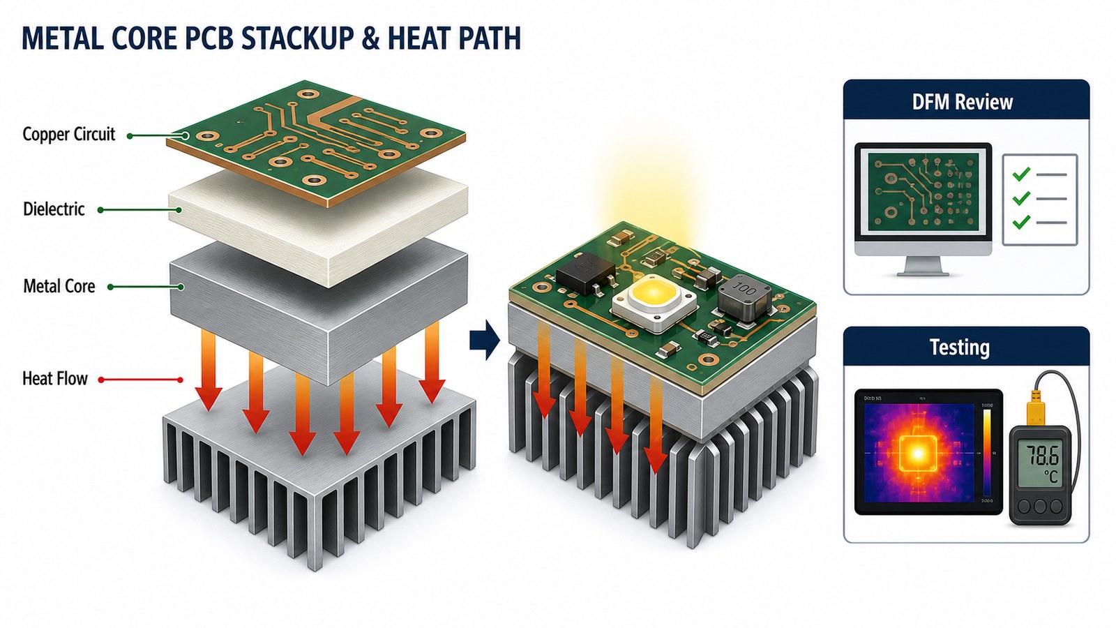
Should assembly lead time be counted separately from PCB fabrication?

For planning, count it as part of the same project schedule. PCB fabrication, component sourcing, SMT scheduling, inspection and final testing affect the delivery date seen by the buyer. A bare board lead time is useful, but it does not describe a finished PCBA order.

When should I use SinkPAD or direct thermal path boards?

Use SinkPAD or another direct thermal path structure when heat must move from a component pad into the metal base more directly than a normal dielectric layer allows. The design should be reviewed early because this structure affects stackup, fabrication route and schedule.

Conclusion

Custom metal-backed PCB lead times are easiest to control when the RFQ is specific, the material path is confirmed and the supplier performs DFM before promising a date. Treat the schedule as an engineering decision: verify the stackup, base metal, thermal path, assembly scope and test plan first, then compare suppliers on confirmed delivery risk instead of headline speed.

You may also like

Wireless Charging MCPCB: Ultra-Thin for Automotive Interior
Thursday, April 23rd, 2026

Ultra-thin wireless charging MCPCB delivers superior thermal conductivity, automotive-grade certifications, and extreme environment reliability. It is ideal for seamless integration into tight automotive interior spaces while maintaining stable high-power wireless charging performance.

Wireless Charging MCPCB, https://www.bestpcbs.com/blog/2026/04/wireless-charging-mcpcb/

Why EBest Stands Out for Wireless Charging MCPCB?

We prioritize your project success by delivering tangible value that reduces costs, accelerates timelines, and minimizes risks. Below are reasons why EBest stands out for wireless charging MCPCB:

  • Quality You Can Trust: We achieve a 99.8% yield rate for wireless charging MCPCB production. This means you receive consistent, defect-free boards that eliminate rework costs and production delays.
  • Fast Lead Times to Keep Your Project On Track: We offer 3–5 day prototype delivery and 7–10 day mass production lead times. This is 30% faster than industry averages, helping you meet tight automotive launch deadlines.
  • Stable Supply Chain for Uninterrupted Production: Our global network of 12+ certified material suppliers ensures 99.5% supply continuity. You won’t face production halts due to material shortages.
  • Dedicated Support to Optimize Your Design: Our engineering team provides free DFM analysis within 24 hours of receiving your design. We identify potential issues early, reducing design iterations by 40% and saving you time and resources.
  • Reliable Performance Guaranteed: Every wireless charging MCPCB undergoes 100% electrical and thermal performance testing. This ensures 0% field failure rates in the first two years of vehicle operation.

Specifications of EBest’s Automotive-Grade Wireless Charging MCPCB

Specification CategoryDetailsAutomotive Application Benefit
Thermal Conductivity2.0–4.0 W/m·KOptimized for high-power heat dissipation during 15W–50W charging
Board Thickness0.4–1.0 mmUltra-thin profile for compact center console and armrest integration
Operating Temperature-40°C to 125°CFully compliant with harsh automotive interior and exterior conditions
Copper Weight1–3 ozSupports high-current wireless charging coils without performance loss
Surface FinishENIGEnsures long-term reliability and solderability for automotive SMT assembly
Wireless Standard ComplianceWPC Qi 1.3, Qi2Fully compatible with all Qi-enabled mobile devices used by drivers and passengers

EBest Certifications & Quality Assurance for Wireless Charging MCPCB

Here are EBest’s certifications and quality assurance for wireless charging MCPCB:

  • IATF 16949 Certification: This automotive-specific quality management system certification ensures full process control throughout production. It eliminates quality risks by standardizing every step from material sourcing to final testing, aligning with global automotive manufacturing requirements.
  • ISO 9001 Certification: Our ISO 9001 certification guarantees consistent manufacturing standards across all batches. This means you receive the same high-quality wireless charging MCPCB every time, ensuring reliable performance in your automotive applications.
  • ISO 13485 Certification: While originally designed for medical devices, this certification extends our quality standards to support high-reliability, zero-failure critical automotive applications. It is ideal for wireless charging MCPCB used in safety-related vehicle systems.
  • AEC-Q100 Certification: Compliant with automotive electronic component reliability requirements, this certification validates that our wireless charging MCPCB can withstand the harsh conditions of automotive environments, including extreme temperatures and vibration.
  • RoHS/REACH Compliance: Our wireless charging MCPCB meets global automotive environmental regulations. This ensures your vehicles comply with regional standards, avoiding costly penalties and expanding your market reach.
  • WPC Qi Certification: Full compliance with WPC Qi 1.3 and Qi2 standards ensures our wireless charging MCPCB works seamlessly with all Qi-enabled devices. This eliminates compatibility issues for end users and enhances the overall vehicle experience.

What Are the Top Pain Points of Wireless Charging MCPCB in Automotive?

Challenge 1: How to prevent excessive heat buildup in tight automotive console spaces for wireless charging MCPCB?

Solution 1: High-thermal-conductivity metal core substrate and optimized thermal via design, which dissipates heat efficiently to prevent performance degradation.

Challenge 2: How to fit wireless charging MCPCB into modern car interiors with limited space for thick PCBs?

Solution 2: Ultra-thin 0.4–1.0 mm profile and flexible design for flush mounting under trim panels, solving the space constraint challenge.

Challenge 3: How to prevent wireless charging MCPCB from causing EMI interference with vehicle electronics?

Solution 3: Integrated magnetic shielding and optimized coil layout that meets automotive EMC standards, eliminating interference with vehicle electronics.

Challenge 4: How to ensure wireless charging MCPCB maintains reliability under extreme automotive temperature cycles?

Solution 4: Automotive-grade materials, a -40°C to 125°C operating range, and passing thermal shock testing to ensure long-term reliability.

Challenge 5: How to improve the charging efficiency of wireless charging MCPCB affected by suboptimal design?

Solution 5: Precision coil patterning and low-loss copper traces, achieving >85% wireless power transfer efficiency to resolve efficiency issues.

Wireless Charging MCPCB, https://www.bestpcbs.com/blog/2026/04/wireless-charging-mcpcb/

How Does Ultra-Thin Wireless Charging MCPCB Improve Automotive Interior Design?

Ultra-thin wireless charging MCPCB is a game-changer for automotive interior design, addressing the industry’s demand for sleek aesthetics, space efficiency, and functional integration. Its slim profile and flexible design allow it to blend seamlessly with modern vehicle interiors, enhancing both visual appeal and user experience without compromising charging performance.

  • Enables flush, seamless integration into center consoles, armrests, and door panels, preserving the sleek, premium aesthetics of modern automotive interiors without bulky protrusions.
  • Eliminates bulky charging modules that waste valuable interior space, creating more room for storage compartments, control panels, or other user-centric features.
  • Supports thin-profile wireless charging pads that blend perfectly with premium interior materials like leather, wood, or carbon fiber, maintaining a cohesive and high-end look.
  • Offers flexible design options to match unique interior layouts, allowing automotive designers to maintain creative freedom without sacrificing wireless charging functionality.
  • Reduces visual clutter in the cabin by integrating charging capabilities directly into existing interior components, avoiding the need for standalone charging devices.
  • Accommodates the trend toward minimalistic automotive interiors, aligning with consumer preferences for clean, uncluttered cabin spaces while adding essential functionality.
  • Facilitates integration with ambient lighting features, allowing the wireless charging MCPCB to complement interior lighting designs and enhance the overall cabin ambiance.

What Thermal Performance Should You Expect from Automotive Wireless Charging MCPCB?

Thermal performance is a critical factor for automotive wireless charging MCPCB, as it directly impacts charging efficiency, component lifespan, and overall reliability in harsh vehicle environments. High-power wireless charging (15W–50W) generates significant heat, so understanding the expected thermal performance helps ensure your MCPCB meets automotive-grade standards and end-user expectations.

  • Thermal conductivity ranges from 2.0–4.0 W/m·K, with our high-end options (4.0 W/m·K) designed to rapidly dissipate heat from high-power wireless charging, preventing performance drops.
  • Maintains stable charging efficiency even in hot cabin environments (up to 60°C), preventing overheating during continuous use in extreme weather conditions.
  • Reduces component temperature by up to 25°C compared to standard PCBs, extending the lifespan of both the wireless charging MCPCB and connected mobile devices.
  • Meets strict automotive thermal standards, passing thermal shock (-40°C to 125°C, 1000 cycles) and thermal aging tests to ensure long-term reliability.
  • Minimizes thermal hotspots through optimized thermal via placement and high-purity aluminum core, ensuring uniform heat distribution across the board.
  • Supports consistent performance during temperature fluctuations, a key requirement for automotive components that operate in varying climates.
  • Complies with AEC-Q100 thermal reliability requirements, ensuring the wireless charging MCPCB performs reliably throughout the vehicle’s service life.
Wireless Charging MCPCB, https://www.bestpcbs.com/blog/2026/04/wireless-charging-mcpcb/

How to Design for Manufacturability (DFM) with Wireless Charging MCPCB?

Designing for manufacturability (DFM) is critical to ensuring your wireless charging MCPCB is cost-effective, reliable, and easy to produce at scale. Here are key best practices tailored to automotive applications:

  • Minimize coil trace width variation: Consistent trace width (±0.05 mm) ensures uniform inductance across the board. This prevents charging efficiency inconsistencies and reduces production defects.
  • Optimize thermal via placement: Place thermal vias directly under coil pads and high-heat components. Space vias 2–3 mm apart to maximize heat transfer to the metal core, reducing hotspots.
  • Use automotive-grade materials compatible with SMT assembly: Choose materials that can withstand high-temperature reflow soldering (260°C for 10 seconds). This ensures compatibility with standard automotive manufacturing processes.
  • Allow sufficient clearance for components: Maintain a minimum 0.5 mm clearance between coil traces and other components. This avoids short circuits and EMI interference with vehicle electronics.
  • Follow IPC-6012 Class 3 standards: These standards ensure high-reliability performance for automotive applications. They cover requirements for dielectric integrity, copper adhesion, and solderability.
  • Integrate FOD (Foreign Object Detection) circuits early: Design FOD sensors into the PCB layout to prevent overheating from metal objects. This complies with automotive safety standards and protects end users.
  • Consult with your manufacturer for DFM feedback: Early DFM analysis (like the free service EBest offers) identifies design flaws before production. This reduces iterations and saves time and costs.

What Are the Material Choices for High-Performance Wireless Charging MCPCB?

Below are material choices for high-performance wireless charging MCPCB:

  • Metal core: Aluminum (Al) with high-purity alloy for optimal thermal transfer. It balances thermal conductivity and cost-effectiveness for automotive applications.
  • Dielectric layer: High-temperature resistant, low-loss epoxy resin. It maintains stability at extreme temperatures and reduces signal loss during charging.
  • Copper foil: Electrodeposited copper, 1–3 oz for low resistance. Thicker copper (3 oz) is ideal for high-power charging applications.
  • Surface finish: ENIG (Electroless Nickel Immersion Gold) for corrosion resistance and solderability. It ensures long-term reliability in harsh automotive environments.
  • Ferrite shielding: Thin, high-permeability sheets to enhance magnetic coupling and reduce EMI. This improves charging efficiency and prevents interference with vehicle systems.

How Does Wireless Charging MCPCB Ensure Reliability in Automotive Environments?

Our wireless charging MCPCB undergoes rigorous automotive reliability testing to ensure performance in harsh conditions:

  • Thermal shock testing (-40°C to 125°C, 1000 cycles) to simulate extreme temperature changes.
  • Vibration testing (per ISO 16750-3) to withstand road vibrations and vehicle movement.
  • Humidity testing (85°C/85% RH, 1000 hours) to prevent moisture damage.
  • Thermal cycling and thermal aging tests to ensure long-term stability.
  • Electrical performance validation under extreme conditions to guarantee consistent charging.

What Customization Options Are Available for Wireless Charging MCPCB?

Here are customization options for wireless charging MCPCB:

  • Board thickness: 0.4–1.0 mm, tailored to your space constraints.
  • Coil design: Single/dual/multi-coil configurations for larger charging areas.
  • Layer count: 1–4 layers for complex circuit integration.
  • Size and shape: Custom profiles to fit specific console designs.
  • Special features: Integrated shielding, thermal vias, LED indicators, FOD circuits.

Automotive Application Case Study: Wireless Charging MCPCB in Premium EV Interiors

Project Requirements

  • A leading premium electric vehicle manufacturer needed a wireless charging MCPCB for their new EV model’s slim center console.
  • Maximum board thickness: 0.6 mm to fit the tight interior space.
  • Thermal conductivity: Minimum 3.0 W/m·K to handle 15W high-power charging without overheating.
  • EMI compliance: Must not interfere with the vehicle’s infotainment and navigation systems.
  • Reliability: Meet AEC-Q100 standards for long-term automotive use.

  • Timeline: Prototype delivery within 4 days, mass production within 8 days to meet vehicle launch deadlines.

EBest’s Solution

  • Designed an ultra-thin 0.6 mm wireless charging MCPCB with 3.0 W/m·K thermal conductivity using high-purity aluminum core.

  • Integrated high-permeability ferrite shielding to minimize EMI interference with vehicle electronics.
  • Optimized coil patterning with 2 oz copper foil to ensure 88% charging efficiency and consistent inductance.
  • Provided free DFM analysis within 24 hours to optimize the design for SMT assembly.
  • Delivered prototypes in 3 days (1 day ahead of schedule) and mass production in 7 days.

Project Output & Results

  • The wireless charging MCPCB fit seamlessly into the slim center console, maintaining the vehicle’s premium interior aesthetics.
  • Operating temperature reduced by 22°C compared to the manufacturer’s previous solution, eliminating overheating issues.
  • EMI emissions were 40% below automotive EMC standards, ensuring no interference with vehicle systems.
  • Charging efficiency reached 88%, exceeding the manufacturer’s 85% target.
  • Yield rate for mass production was 99.9%, eliminating rework costs and production delays.
  • The solution helped the manufacturer meet their vehicle launch deadline and receive positive feedback from end users.
Wireless Charging MCPCB, https://www.bestpcbs.com/blog/2026/04/wireless-charging-mcpcb/

FAQ About Wireless Charging MCPCB

Q1: What is the minimum thickness available for EBest’s wireless charging MCPCB?

A1: The minimum thickness for EBest’s wireless charging MCPCB is 0.4 mm. This ultra-thin profile is ideal for ultra-slim automotive interior integration, including tight center consoles and armrests.

Q2: Does your wireless charging MCPCB support Qi 1.3 and Qi2 standards?

A2: Yes, our wireless charging MCPCB is fully designed to support WPC Qi 1.3 and Qi2 standards. It includes compatibility with 15W EPP and higher power profiles, ensuring seamless use with all Qi-enabled mobile devices.

Q3: What is the operating temperature range for automotive-grade wireless charging MCPCB?

A3: Our automotive wireless charging MCPCB operates reliably from -40°C to 125°C. This range meets AEC-Q100 requirements and ensures performance in extreme hot and cold automotive environments.

Q4: How does your wireless charging MCPCB handle EMI in automotive environments?

A4: We integrate optimized ferrite shielding and controlled impedance design to minimize EMI. Our solution ensures compliance with automotive EMC standards, preventing interference with vehicle infotainment, navigation, and safety systems.

Q5: What is the typical lead time for prototype and mass production of wireless charging MCPCB?

A5: Prototype lead time is 3–5 days. Mass production lead time is 7–10 days. We also offer expedited options for urgent projects, helping you meet tight launch deadlines.

Q6: Can you customize coil patterns for specific automotive charging pad designs?

A6: Yes, we provide full custom coil design and patterning services. Our engineering team works with you to match your exact charging area, power requirements, and interior design constraints.

Q7: What quality testing do you perform on wireless charging MCPCB before shipment?

A7: We conduct 100% electrical testing, thermal performance validation, and visual inspection for every board. We also perform sample-level reliability testing per automotive standards, including thermal shock and vibration tests.

How to Source Reliable Wireless Charging MCPCB for Automotive Projects?

Follow these steps to ensure you source a high-quality, reliable wireless charging MCPCB for your automotive project:

  1. Define your requirements clearly. This includes thickness, thermal conductivity, power level, size, and required certifications.
  2. Request DFM analysis from your manufacturer. This helps optimize your design for manufacturability and reduces production issues.
  3. Validate prototype performance with thermal and electrical testing. Ensure it meets your project’s specific requirements.
  4. Confirm supply chain stability and production capacity. Choose a manufacturer with a proven track record of consistent delivery.
  5. Establish quality control protocols aligned with automotive standards. This ensures consistent performance across all batches.
  6. Partner with a manufacturer with proven automotive electronics experience. This reduces risks and ensures compliance with industry standards.

Ready to Order Your Custom Wireless Charging MCPCB from EBest?

EBest delivers high-quality, ultra-thin wireless charging MCPCB tailored for automotive interior applications. Take advantage of our batch order exclusive support, including dedicated engineering oversight and volume pricing and rapid prototype turnaround (3–5 days) to accelerate your automotive wireless charging project. Don’t miss your vehicle launch deadline. Contact us today at sales@bestpcbs.com to discuss your requirements and place your order before our limited production slots fill up.

You may also like