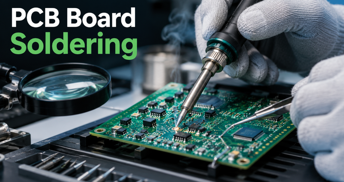
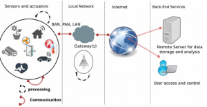
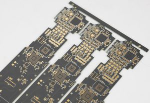
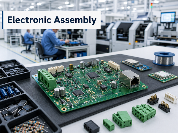
In the electronics manufacturing field, e assembly is usually understood as electronic assembly or electronics assembly. It refers to the process of turning bare circuit boards, components, cables, connectors, and sometimes enclosures into working electronic products. For many customers, especially hardware developers and purchasing teams, electronic assembly mainly refers to PCB assembly, also called PCBA assembly.
A well-planned electronic assembly project includes BOM review, component sourcing, process control, inspection, electrical testing, packaging, and production traceability. If the early engineering data is clear, the assembly supplier can quote faster, reduce production questions, and avoid preventable defects.
What Is Electronic Assembly?
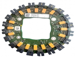
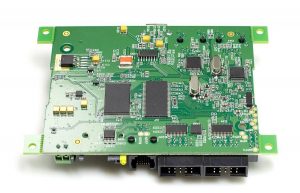
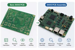
Electronic assembly is the manufacturing process of installing electronic components onto a circuit board or into an electronic product. In PCB-related projects, it usually starts with a fabricated bare PCB and ends with an assembled circuit board that can be tested, programmed, and integrated into a device.
A typical electronic assembly project may include SMT placement, through-hole insertion, soldering, cleaning, inspection, functional testing, conformal coating, cable connection, and final product assembly. The actual scope depends on how much work the customer wants the manufacturer to handle.
Is Electronic Assembly the Same as PCB Assembly?
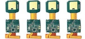
Electronic assembly and PCB assembly are closely related, but they are not exactly the same. PCB assembly focuses on mounting and soldering components onto a printed circuit board. Electronic assembly is broader and may include board-level assembly, wire harnesses, module integration, firmware loading, testing, labeling, and box build assembly.
If the work ends at the assembled board, it is usually PCB assembly. If the work continues into cables, housing, displays, keypads, batteries, or final product integration, it becomes electronic assembly.
| Item | PCB Assembly | Electronic Assembly |
|---|---|---|
| Main scope | Component mounting on PCB | Board, wiring, enclosure, and product integration |
| Output | PCBA | PCBA, module, or finished electronic product |
| Common process | SMT, DIP, soldering, inspection | PCBA, cable assembly, programming, testing, box build |
| Customer files needed | Gerber, BOM, pick-and-place, assembly drawing | PCB files plus mechanical drawings, test procedures, firmware, labels |
| Typical buyer | PCB designer, hardware engineer, purchasing team | OEM, product developer, system integrator |
What Are the Main Types of Electronic Assembly?
Different assembly types are used because products have different requirements for size, strength, cost, volume, and reliability. A compact IoT board, a power controller, and an industrial control box should not use the same assembly strategy.
| Assembly Type | Best Used For | Practical Notes |
|---|---|---|
| SMT assembly | Compact, high-density electronic boards | Suitable for ICs, resistors, capacitors, LEDs, sensors, and fine-pitch parts |
| Through-hole assembly | Connectors, relays, transformers, power parts | Provides stronger mechanical support than surface mounting |
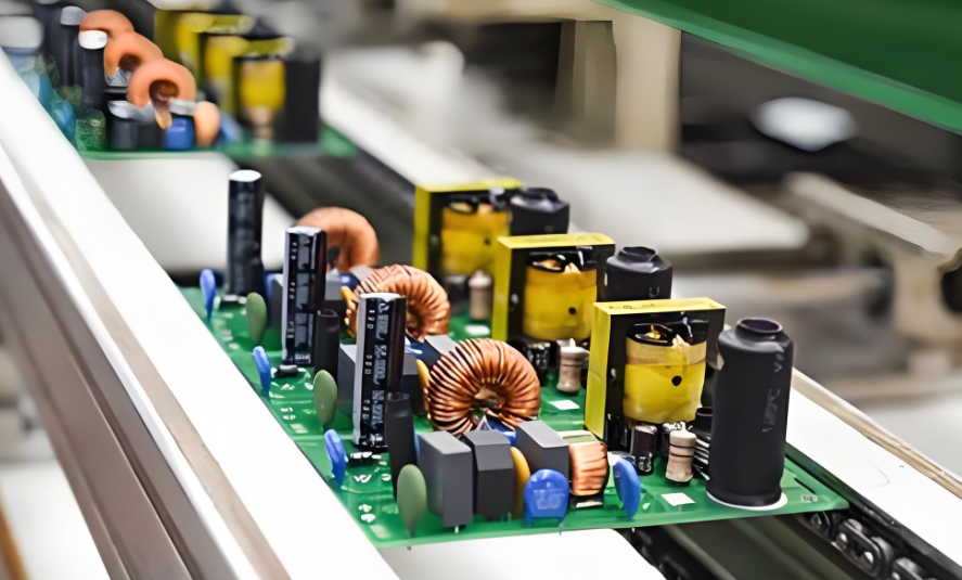
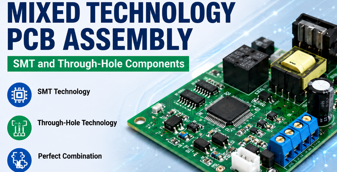
| Mixed assembly | Boards with both SMT and through-hole parts | Common in industrial, power, automotive, and control electronics |
| Turnkey assembly | Customers who want one supplier to manage PCB, parts, and assembly | Requires a clear BOM, approved alternatives, and sourcing rules |
| Box build assembly | Final product or module integration | Needs mechanical drawings, wiring instructions, labels, and test steps |
Most modern products use mixed assembly. SMT handles compact electronic functions, while through-hole parts are kept for components that face plugging force, vibration, high current, or mechanical stress.
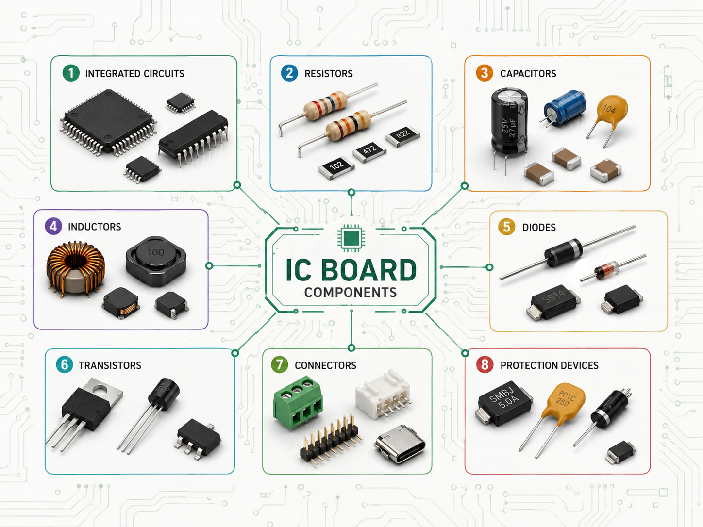
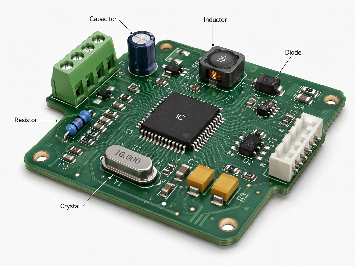
What Components Are Used in Electronic Assembly?
Electronic assembly uses different components depending on the circuit function, product size, power level, and reliability requirements. Common components include:
- Resistors: Control current, divide voltage, and set circuit values.
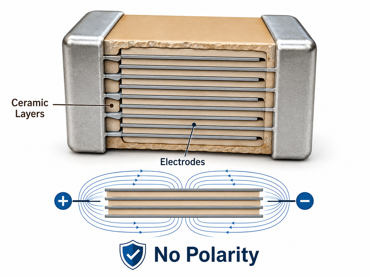
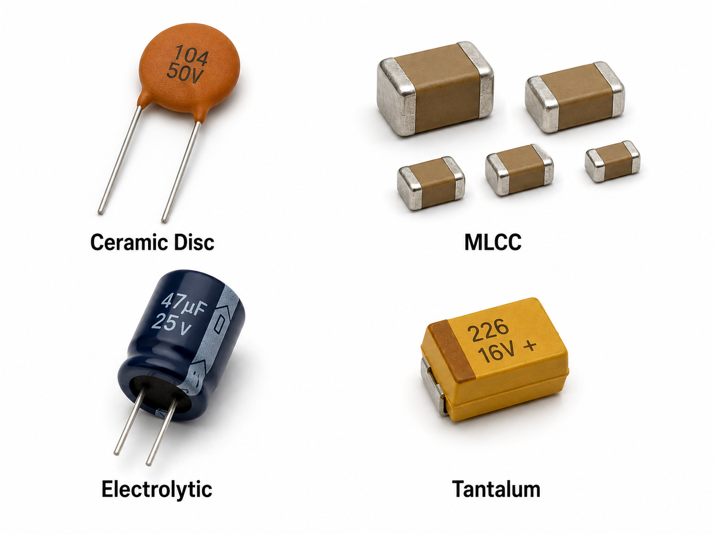
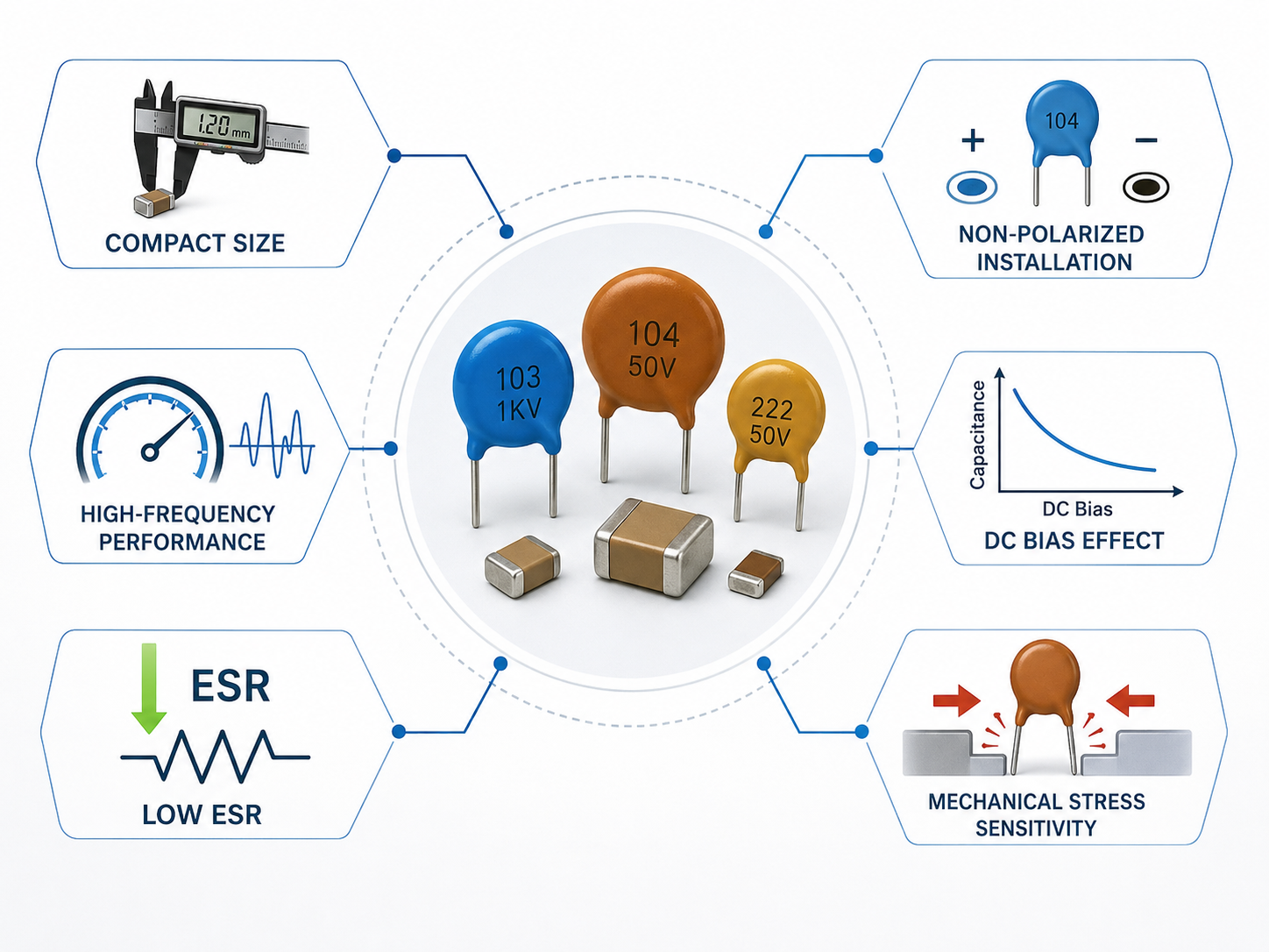
- Capacitors: Store energy, filter noise, and stabilize power supply lines.
- Inductors: Used in filters, power circuits, and EMI control.
- Diodes and LEDs: Support rectification, protection, lighting, and status indication.
- Transistors and MOSFETs: Used for switching, amplification, and power control.
- Integrated circuits: Handle processing, memory, communication, sensing, and power management.
- Connectors: Provide power, signal, programming, and cable connections.
- Relays and switches: Used for control, user input, and load switching.
- Sensors: Detect temperature, motion, pressure, light, humidity, or current.
- Fuses and protection devices: Protect circuits from overcurrent, ESD, and voltage surges.
- Modules: Used for wireless communication, GPS, Bluetooth, Wi-Fi, or power conversion.
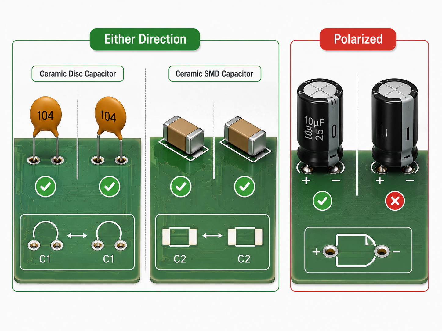
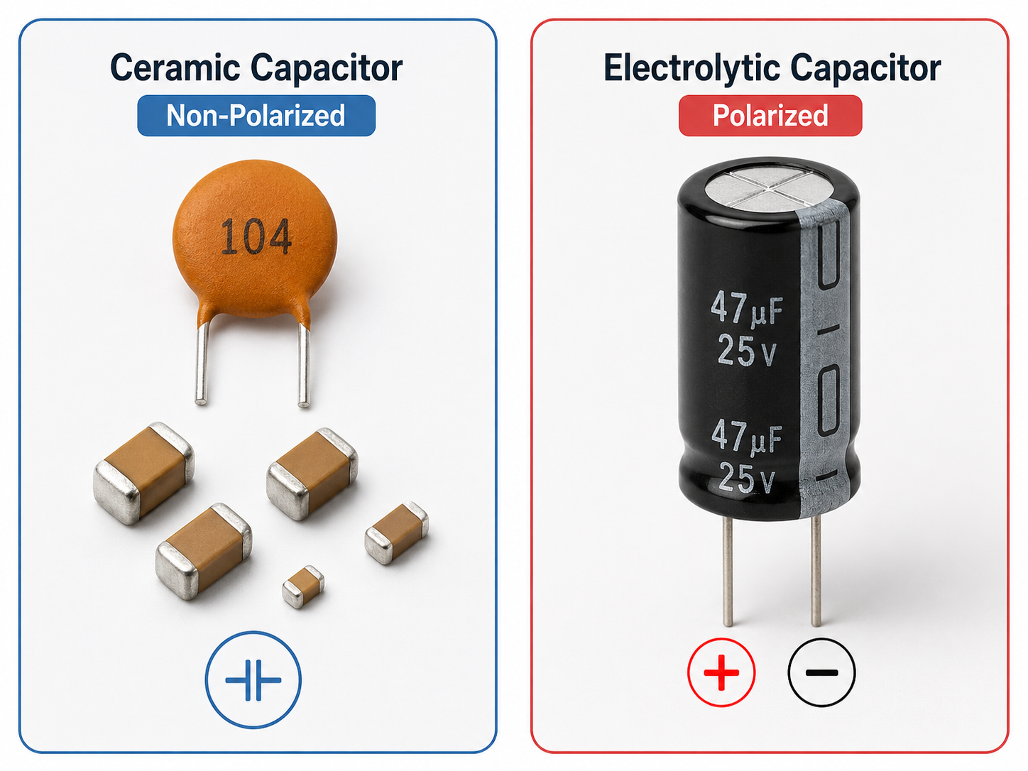
For PCB assembly quotation, the BOM should include part number, package size, value, tolerance, voltage rating, polarity, and approved alternatives. Clear component information helps avoid sourcing mistakes and assembly delays.
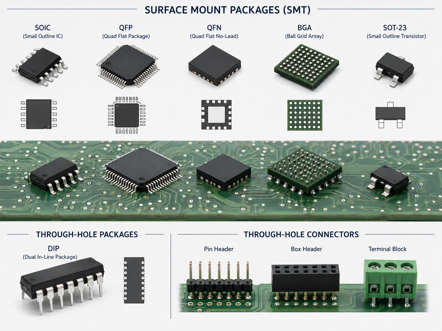
Why Is SMT Assembly Important in Modern Electronics?
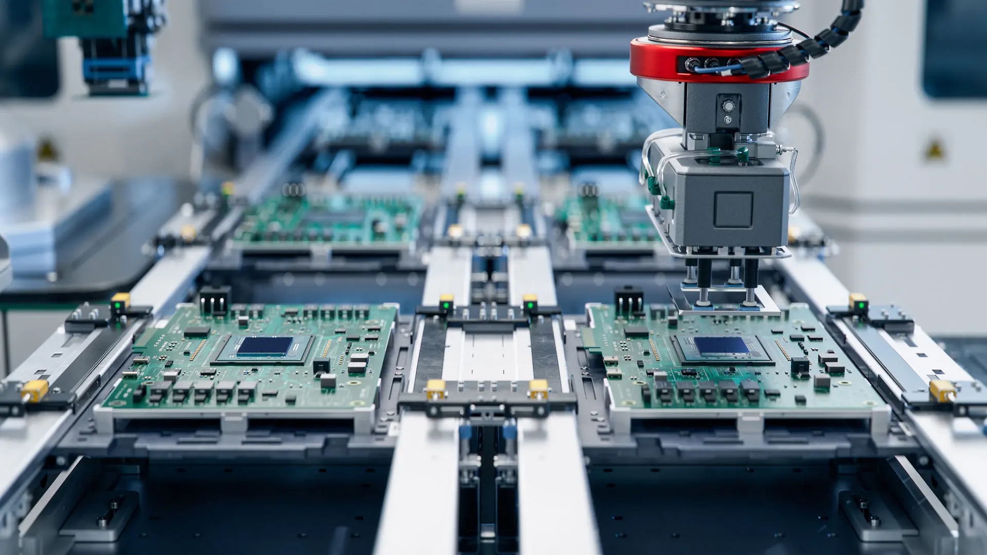
SMT assembly is important because most modern electronic products need compact size, repeatable production, and high component density. Surface mount components can be placed quickly by automated machines, which makes SMT suitable for prototypes, medium-volume production, and mass production.
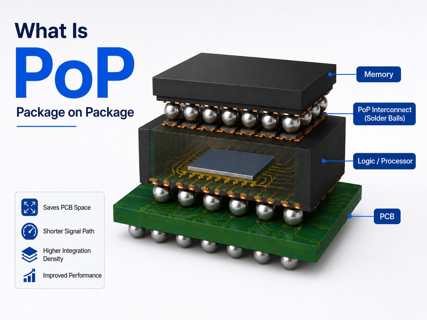
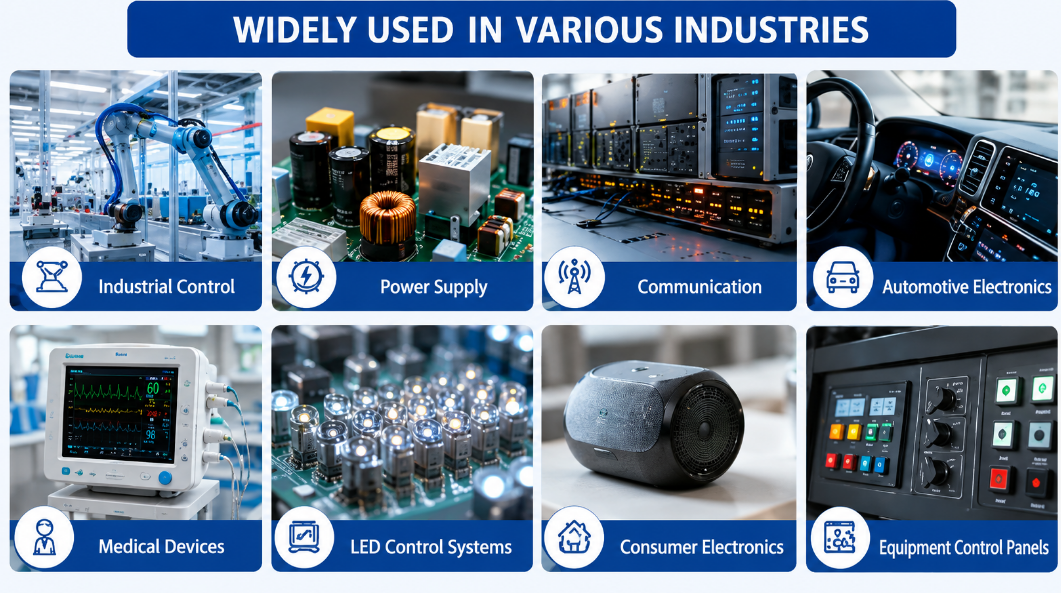
SMT is especially useful for products such as communication devices, IoT modules, LED drivers, industrial controllers, consumer electronics, medical devices, and automotive electronics. It supports small passive packages, fine-pitch ICs, QFNs, BGAs, and high-density layouts that are difficult to build with through-hole technology alone.
However, SMT is not automatically the best choice for every component. Large connectors, high-current terminals, heavy magnetic parts, and mechanically stressed parts may still need through-hole mounting or additional mechanical support. Good assembly planning uses SMT where density and automation matter, and through-hole where mechanical strength is more important.
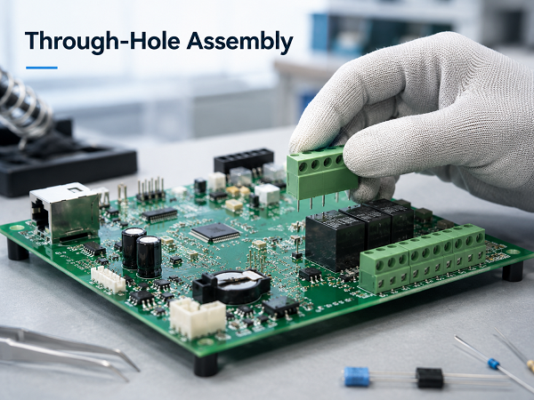
When Is Through-Hole Assembly Still Needed?
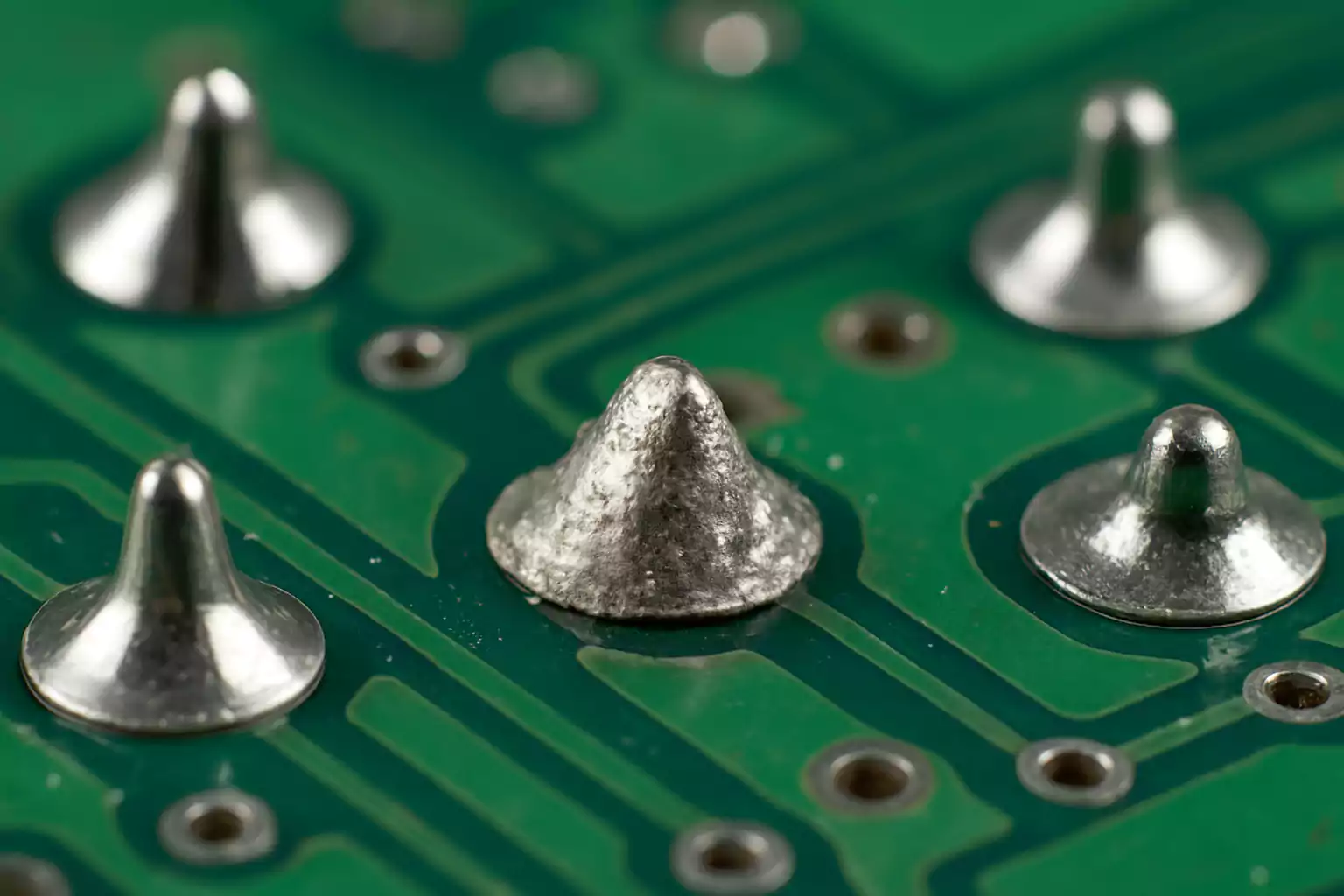
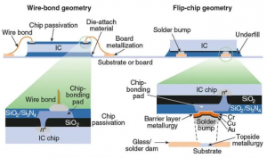
Through-hole assembly is still valuable when the component needs stronger board retention or better resistance to plugging force, vibration, pulling, or thermal cycling. The component leads pass through plated holes and are soldered on the opposite side, creating a stronger joint than many surface-mounted alternatives.
Typical through-hole components include terminal blocks, pin headers, relays, transformers, large electrolytic capacitors, power connectors, switches, fuses, and some high-current components. These parts often appear in industrial controls, power supplies, automotive modules, home appliances, and equipment with external cable connections.
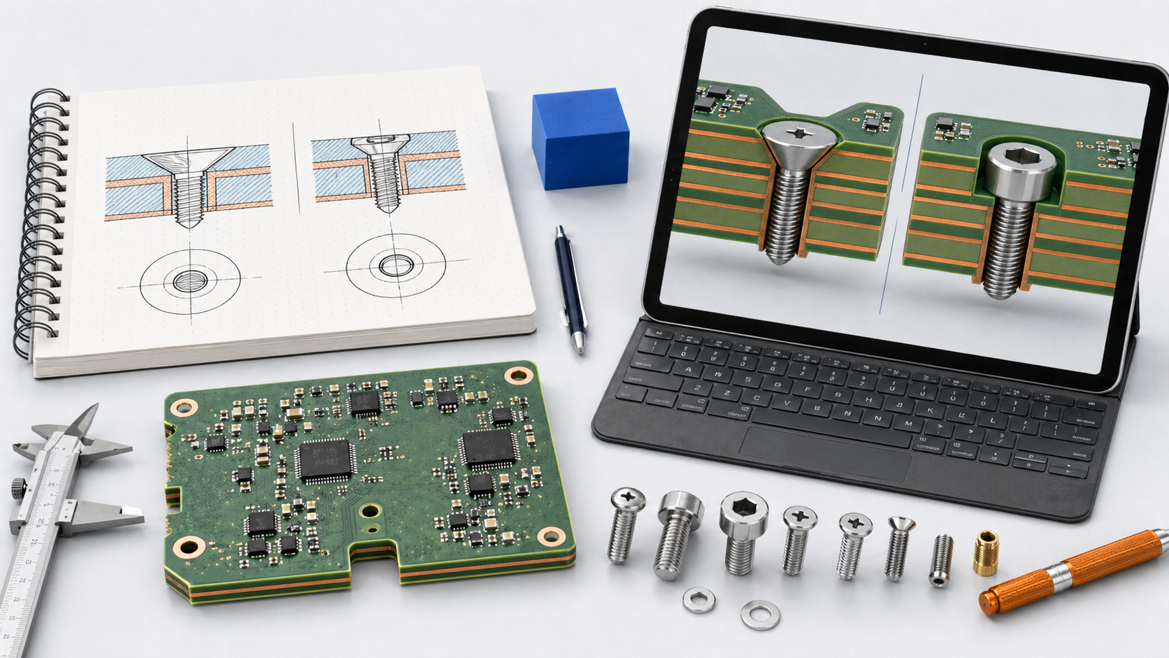
What Files Are Needed for Electronic Assembly?
Clear production files reduce quotation questions and prevent assembly mistakes. Missing or inconsistent files can cause wrong component placement, polarity errors, delayed sourcing, or incorrect test expectations.
| File | Why It Matters |
|---|---|
| Gerber files | Defines PCB copper layers, solder mask, silkscreen, drill data, and board outline |
| BOM | Lists all components needed for assembly and sourcing |
| Pick-and-place file | Provides component coordinates, side, and rotation |
| Assembly drawing | Shows placement reference, polarity, orientation, and special notes |
| PCB fabrication notes | Defines material, thickness, copper weight, surface finish, impedance, and tolerance |
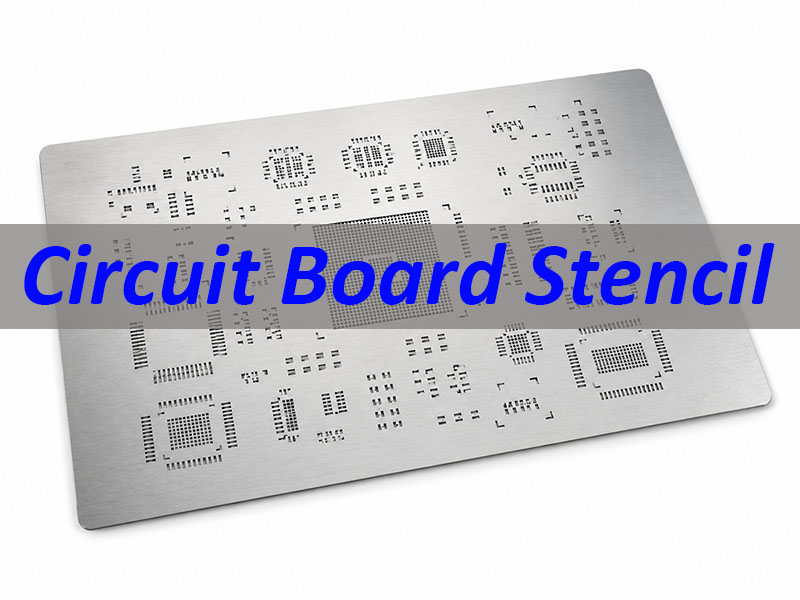
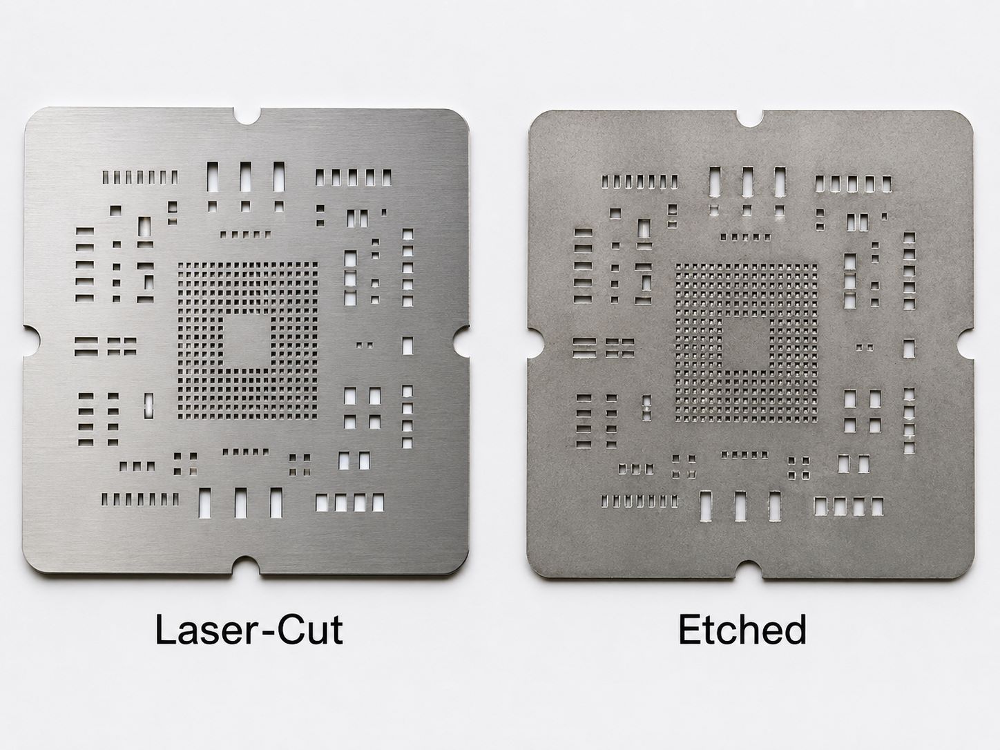
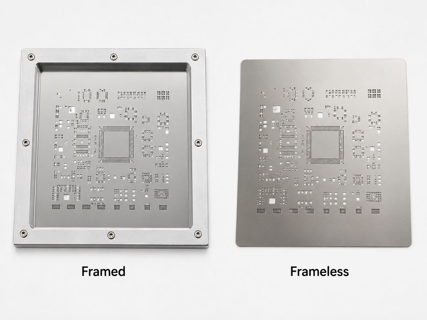
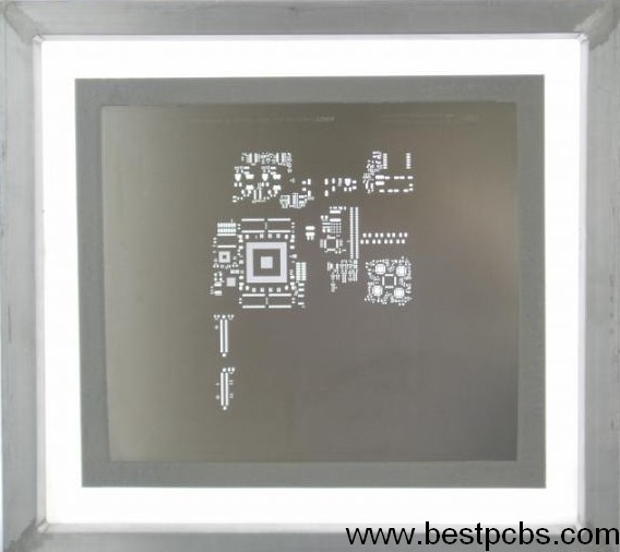
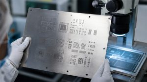
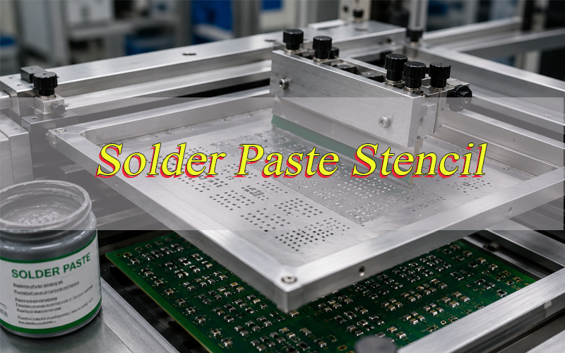
| Stencil requirement | Helps control solder paste volume for SMT assembly |
| Test procedure | Defines how the board should be tested and what result is acceptable |
| Firmware file | Needed if IC programming or module configuration is required |
| Mechanical drawing | Required for box build, enclosure fitting, connector alignment, or cable assembly |
| Approved vendor list | Controls which component brands or suppliers may be used |
For a fast quote, customers should send Gerber, BOM, pick-and-place, assembly drawing, quantity, lead time target, and testing requirements together. For turnkey electronic assembly, the BOM should be especially detailed because sourcing quality directly affects cost, delivery, and long-term reliability.
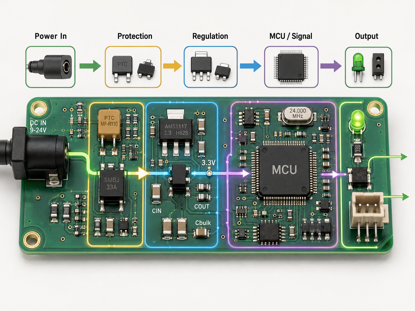
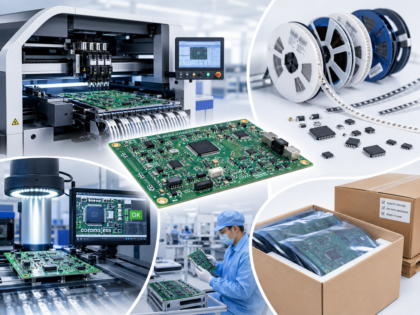
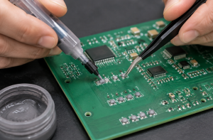
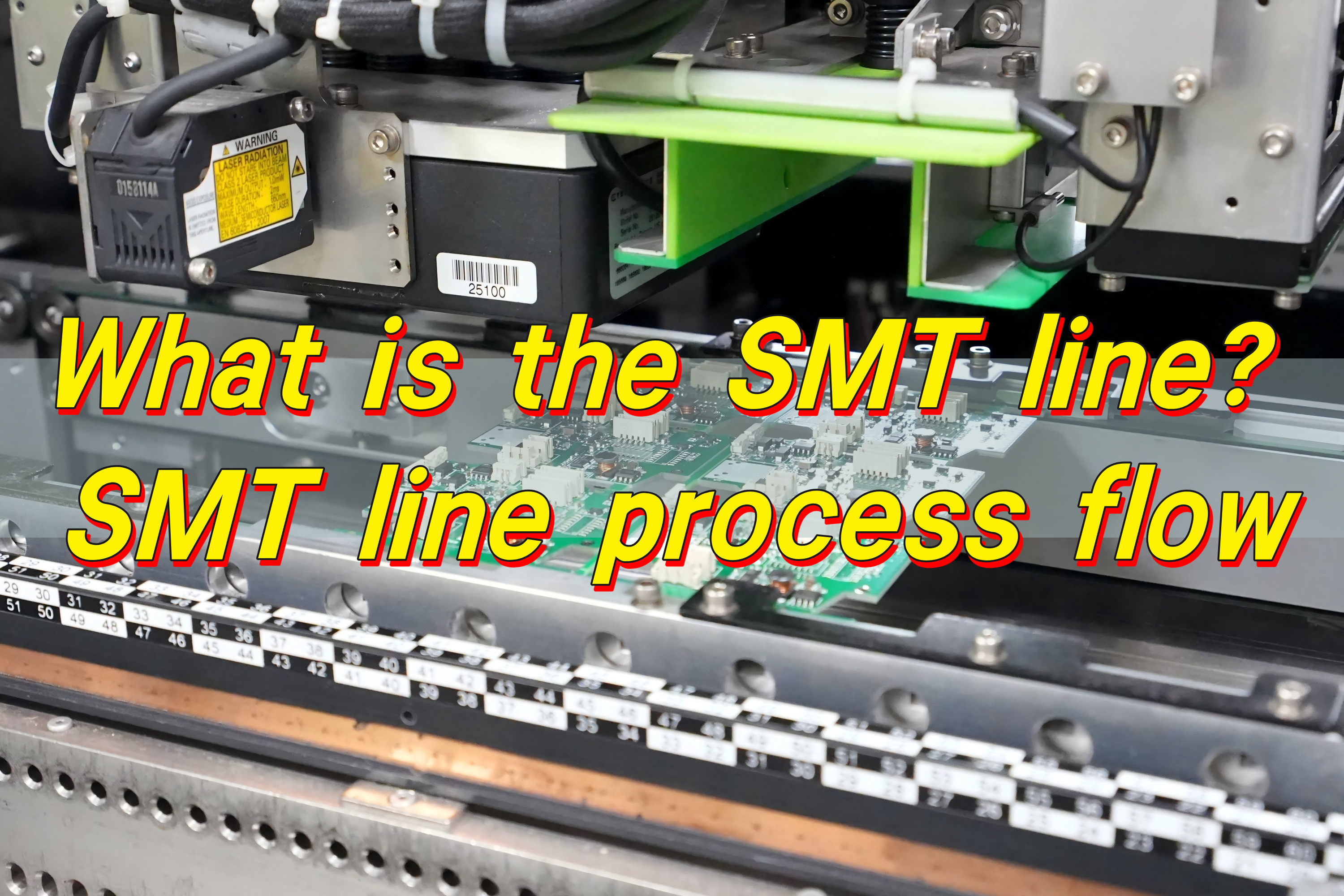
How Does the Electronic Assembly Process Work?
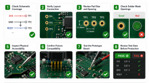
A reliable electronic assembly process starts before production. The manufacturer needs to check whether the PCB layout, BOM, package data, and test method match real production conditions.
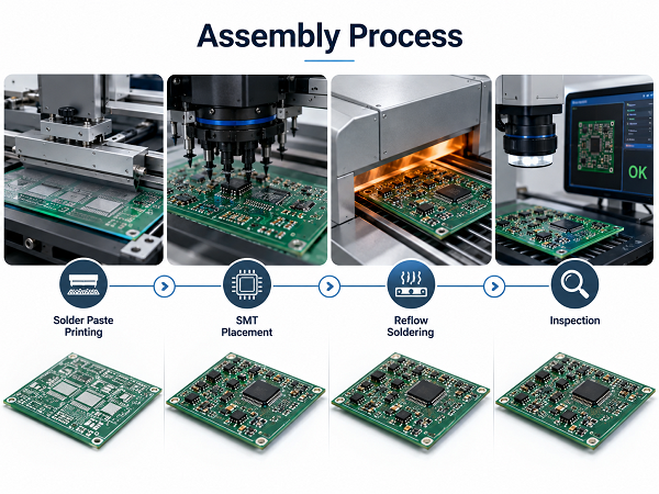
A common process includes:
- Engineering data review
The supplier checks Gerber files, BOM, pick-and-place data, polarity marks, package footprints, and assembly drawings. This step helps identify missing values, wrong package sizes, unclear part orientation, or component lifecycle risks. - DFM and DFA review
DFM checks PCB manufacturability, while DFA checks whether the board can be assembled efficiently. Useful review points include fiducial position, component spacing, solder mask clearance, BGA escape routing, panelization, and connector accessibility. - Component sourcing
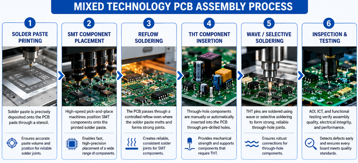
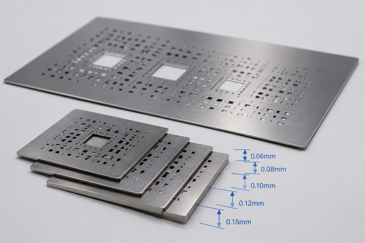
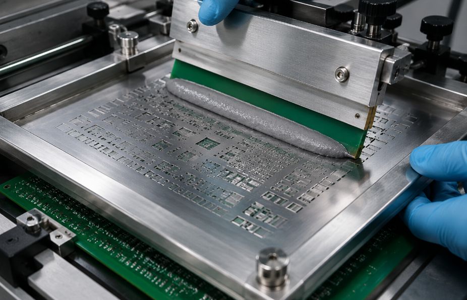
Components are purchased according to the BOM. For stable purchasing, the BOM should include manufacturer part number, package, value, tolerance, voltage rating, temperature rating, and approved substitutes where possible. - Solder paste printing
A stencil deposits solder paste onto PCB pads. Aperture design matters for fine-pitch ICs, QFNs, BGAs, small passives, and thermal pads. Poor stencil design can cause solder bridging, insufficient solder, or excessive voiding. - SMT placement
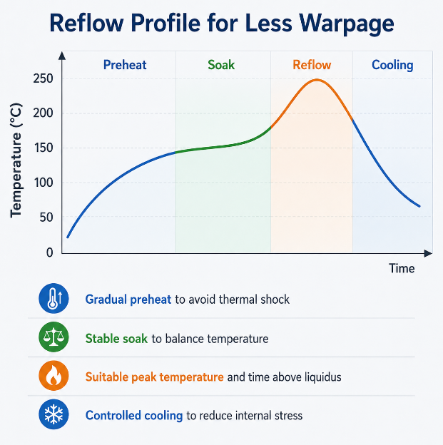
Pick-and-place machines mount SMD parts according to the placement file. Correct rotation and polarity are critical for diodes, LEDs, ICs, electrolytic capacitors, connectors, and sensor modules. - Reflow soldering
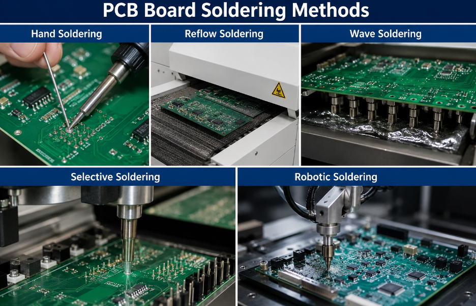
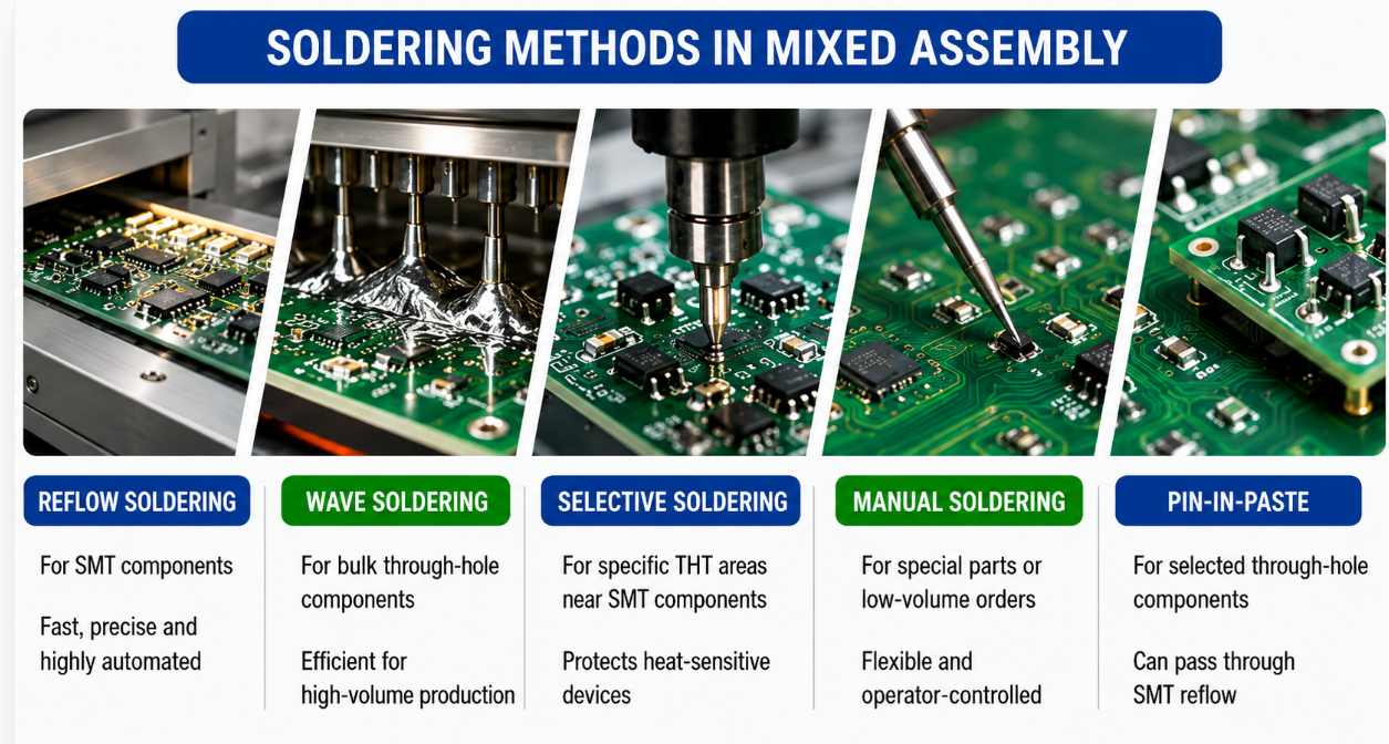
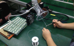
The PCB passes through a controlled temperature profile. The profile must match solder paste type, component heat tolerance, board thickness, copper weight, and thermal mass. - Through-hole assembly
DIP components are inserted after SMT if the board uses connectors, transformers, relays, terminal blocks, or large capacitors. Soldering may use wave soldering, selective soldering, or manual soldering depending on design and quantity. - Inspection and testing
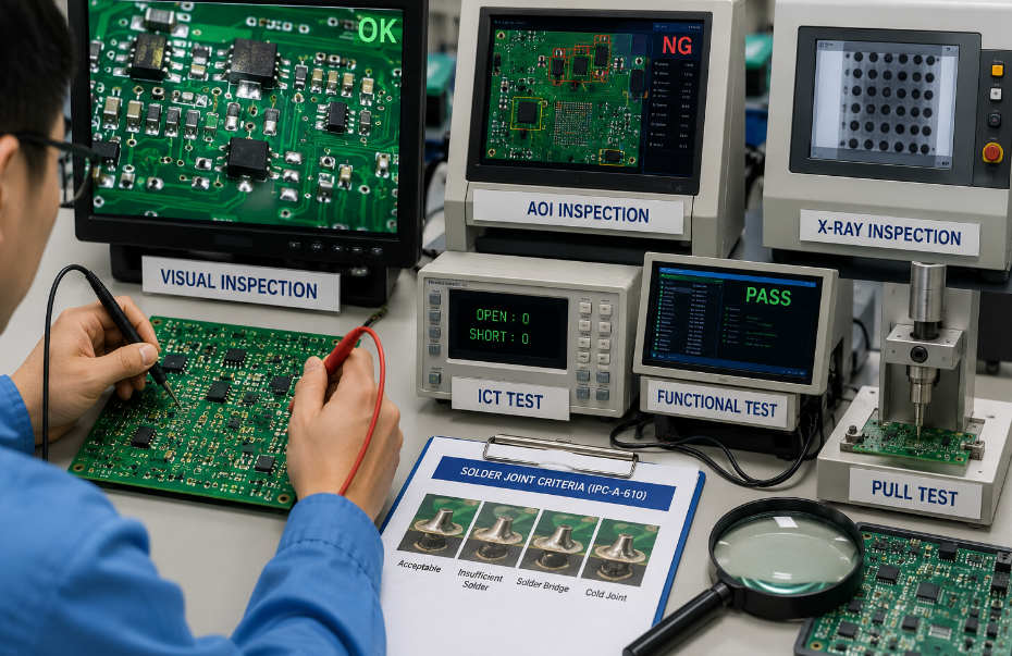
AOI, X-ray, ICT, flying probe, or functional testing may be used. The right inspection method depends on component type, board complexity, and reliability requirements. - Final operations
The board may need cleaning, conformal coating, firmware programming, labeling, cable connection, or box build assembly before shipment.
The most effective projects provide test instructions early. If the test method is only discussed after assembly, fixtures, programming tools, and pass/fail criteria may delay delivery.
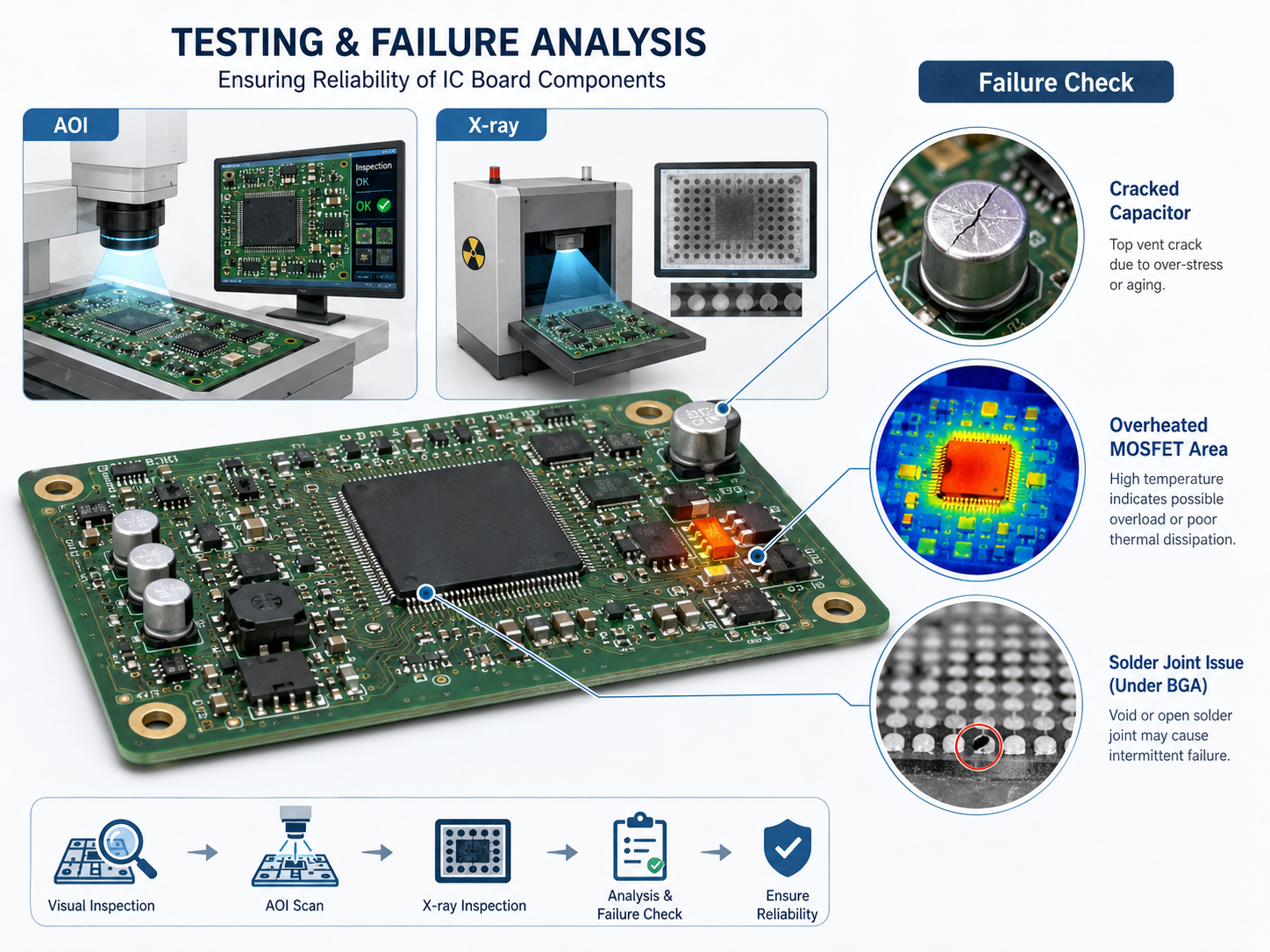
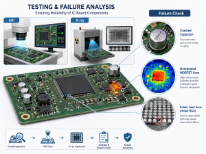
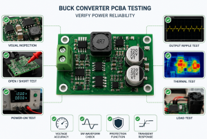
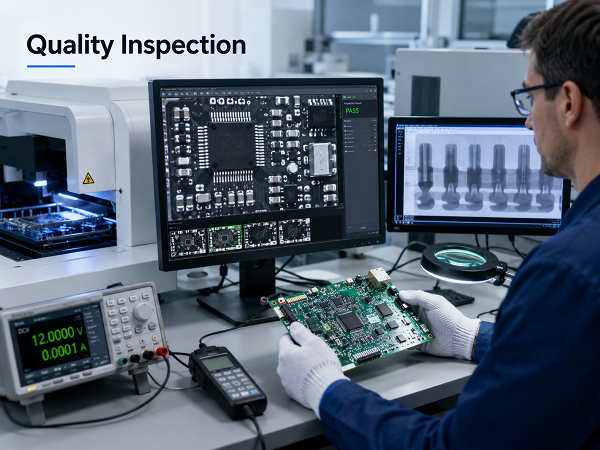
What Quality Checks Are Used in Electronic Assembly?
Quality checks should match the board’s complexity and risk level. A simple LED board may not need the same inspection plan as a BGA-based medical control board or automotive power module.
Common inspection and testing methods include:
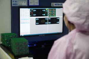
- SPI: Checks solder paste volume and position before component placement.
- AOI: Detects missing parts, polarity errors, skewed components, solder bridges, and visible solder defects.
- X-ray inspection: Used for hidden solder joints such as BGA, QFN, LGA, and some bottom-terminated components.
- First article inspection: Confirms the first assembled board against the BOM, drawing, and approved sample.
- ICT or flying probe testing: Checks electrical continuity, shorts, opens, resistance, and basic circuit conditions.
- Functional testing: Verifies whether the assembled board performs as intended in a real or simulated operating condition.
- Aging or burn-in test: Useful for products that must operate under load for a defined period before shipment.
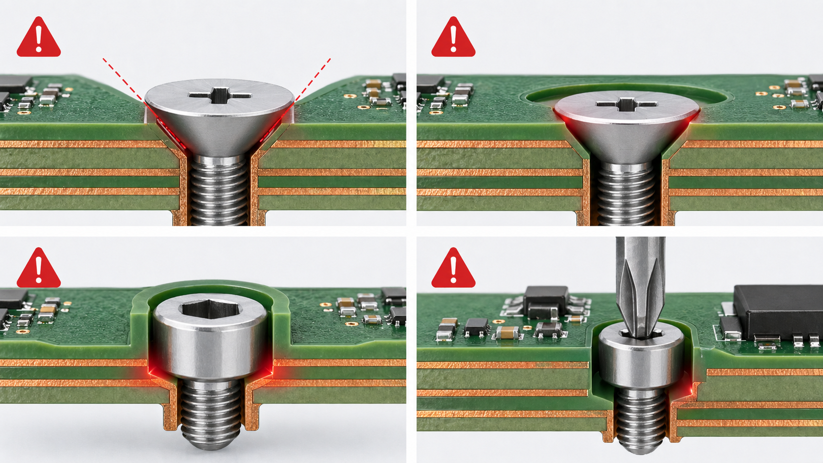
What Are Common Electronic Assembly Defects?
Most electronic assembly defects come from mismatched design data, unsuitable solder paste control, wrong component handling, poor thermal balance, or unclear production instructions. The earlier these risks are checked, the easier they are to prevent.
Common defects include solder bridges, tombstoning, insufficient solder, cold joints, wrong component values, missing parts, reversed polarity, lifted leads, BGA voiding, poor wetting, component cracking, connector misalignment, and flux residue.
Small passive parts can tombstone when pad design or thermal balance is uneven. Fine-pitch ICs can bridge when stencil openings deposit too much solder. QFN and power packages may show voids if the thermal pad design or reflow profile is not controlled. Connectors may shift if there is no mechanical alignment feature or if manual soldering is not supported by fixtures.
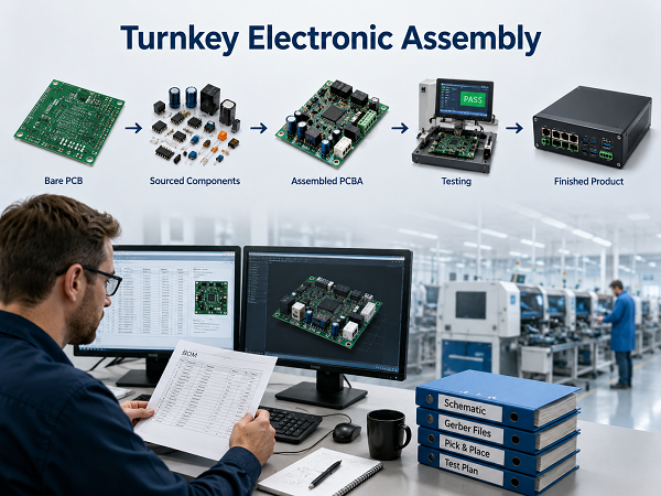
What Is Turnkey Electronic Assembly?
Turnkey electronic assembly means the manufacturer manages most or all production steps, including PCB fabrication, component sourcing, SMT assembly, through-hole assembly, inspection, testing, and sometimes box build assembly. It is useful when customers want fewer suppliers, simpler communication, and better coordination between PCB production and assembly.
Turnkey assembly is especially helpful for startups, engineering teams without internal purchasing support, and overseas buyers who want one manufacturer to manage fabrication and assembly together. It can also reduce mismatch problems between PCB fabrication and assembly because the same supplier can review stencil, panelization, surface finish, solderability, and component fit before production.
What Is the Difference Between Prototype and Mass Production Electronic Assembly?
Prototype and mass production assembly have different goals. Prototype assembly focuses on design validation and quick correction. Mass production focuses on stable yield, repeatability, cost control, and process documentation.
| Item | Prototype Electronic Assembly | Mass Production Electronic Assembly |
|---|---|---|
| Main goal | Verify design and function | Build stable products repeatedly |
| Quantity | Small batch | Medium to high volume |
| BOM status | May still change | Should be controlled and approved |
| Process setup | More flexible | More standardized |
| Testing | Often engineering-focused | Must be repeatable and documented |
| Cost focus | Speed and learning | Yield, efficiency, and unit cost |
| Risk control | Finds design or sourcing issues early | Prevents batch defects and variation |
For prototypes, customers should expect engineering questions and possible design improvements. For mass production, the design, BOM, test procedure, packaging, and acceptance criteria should be frozen before release. Moving to mass production too early can create avoidable cost if the board still has footprint errors, unstable components, or unclear test standards.
How to Choose an Electronic Assembly Manufacturer?
Choosing an electronic assembly manufacturer should be based on technical fit, communication quality, sourcing control, testing capability, and production range. The cheapest quote is not always the best choice if the project includes fine-pitch ICs, BGAs, mixed assembly, conformal coating, or product-level testing.
| Selection Factor | What Customers Should Check |
|---|---|
| PCB capability | Layer count, material options, copper thickness, impedance control, surface finish |
| SMT capability | Package size, BGA/QFN experience, placement accuracy, stencil control |
| Through-hole capability | Wave soldering, selective soldering, fixture support, manual soldering quality |
| Component sourcing | Original channels, substitute control, shortage handling, lifecycle awareness |
| Testing support | AOI, X-ray, ICT, flying probe, functional testing, aging test |
| Engineering review | BOM check, DFM, DFA, polarity review, panelization advice |
| Quality system | Traceability, inspection records, process control, standard operating procedures |
| Project range | Prototype, low-volume, high-mix, and volume production support |
| Communication | Fast engineering feedback, clear EQ handling, accurate quotation details |
A practical supplier should ask useful questions before production, not after defects appear. Good questions may involve unclear polarity, missing package data, solder mask opening, component substitutions, test fixture availability, and whether the product needs cleaning, coating, programming, or special packaging.
How EBest Circuit Supports Electronic Assembly Projects
EBest Circuit supports electronic assembly projects by combining PCB fabrication, component sourcing, SMT assembly, through-hole assembly, testing, and value-added PCBA services in one workflow. This is useful for customers who need both bare PCB production and assembled board delivery without coordinating multiple suppliers.
For PCB and PCBA projects, the team can review Gerber files, BOMs, pick-and-place data, and assembly drawings before quotation. This helps customers identify missing component information, footprint mismatch, unclear polarity, or manufacturing risks early. For boards with BGA, fine-pitch ICs, heavy copper areas, metal core substrates, ceramic PCB requirements, or mixed assembly, early engineering communication can reduce trial-and-error during production.
FAQs
What does electronic assembly mean?
Electronic assembly means building electronic products or modules by installing components, soldering connections, inspecting boards, testing functions, and sometimes integrating cables, housings, displays, batteries, or other product parts.
What is the difference between PCB and PCBA?
A PCB is a bare printed circuit board without components. A PCBA is the board after components have been mounted and soldered. PCBA is the functional assembly used inside the final electronic product.
What is included in electronic assembly services?
Electronic assembly services may include SMT assembly, through-hole assembly, component sourcing, inspection, X-ray, functional testing, IC programming, cleaning, conformal coating, cable assembly, and box build assembly.
Is SMT better than through-hole assembly?
SMT is better for compact size, automated production, and high-density layouts. Through-hole assembly is better for components that need stronger mechanical support, such as large connectors, relays, transformers, and terminal blocks.
What files are needed for PCB assembly?
The basic files include Gerber, BOM, pick-and-place file, and assembly drawing. For tested or turnkey projects, customers should also provide test procedures, firmware, approved vendor lists, and mechanical drawings if needed.
How do you test an assembled PCB?
An assembled PCB can be tested by visual inspection, AOI, X-ray, flying probe, ICT, functional testing, or burn-in testing. The best method depends on board complexity, component type, and reliability requirements.
What is turnkey electronic assembly?
Turnkey electronic assembly means the manufacturer handles PCB fabrication, component purchasing, assembly, inspection, and sometimes testing or box build service. It reduces supplier coordination but requires accurate BOM and production files.
How long does electronic assembly take?
Lead time depends on PCB complexity, component availability, assembly quantity, testing requirements, and whether fixtures or firmware programming are needed. Component sourcing often has more impact on lead time than the assembly process itself.
Can electronic assembly include box build service?
Yes. Box build assembly may include installing the PCBA into an enclosure, connecting cables, mounting displays or keypads, applying labels, loading firmware, and performing final product tests.
How do I choose a reliable electronic assembly supplier?
Choose a supplier based on PCB capability, SMT experience, component sourcing control, inspection equipment, testing support, engineering communication, and experience with your product type. For complex boards, technical fit is usually more important than the lowest unit price.
Conclusion
Electronic assembly is the bridge between circuit design and a working electronic product. Customers can make better purchasing decisions by understanding assembly types, required files, testing options, common defects, and supplier capabilities.
For PCB assembly, turnkey PCBA, component sourcing, or electronic assembly support, you can contact EBest Circuit at sales@bestpcbs.com.