Build It Right the First Time
Gerber, NC drill, line width, spacing, solder mask, board outline, stack-up, and special notes are reviewed before fabrication.



PCB prototype fabrication with no MOQ, DFM review, quick-turn support, special substrate options, and a clear path from prototype to small batch or volume production.
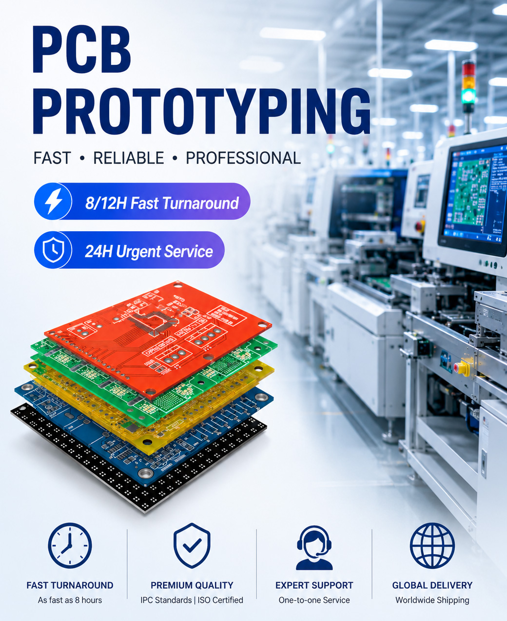
Reduce the chance of prototype failure, schedule delay, and quality uncertainty before fabrication starts.
Gerber, NC drill, line width, spacing, solder mask, board outline, stack-up, and special notes are reviewed before fabrication.
Schedule is confirmed according to layers, material, copper thickness, finish, board complexity, testing, and urgent needs.
Control points include dimensional tolerance, hole copper, impedance, solder mask, surface finish, warpage, and consistency.
HDI, flex, rigid-flex, aluminum, ceramic, high Tg, heavy copper, impedance boards, and fine-pitch BGA designs are supported.
Support for standard and advanced prototype boards, helping engineering teams verify design intent before moving into small batch or volume production.
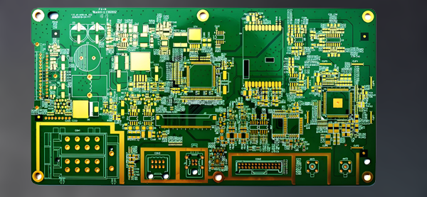
Prototype support for 4-layer, 6-layer, 8-layer, and higher-layer boards with stack-up and manufacturability review.
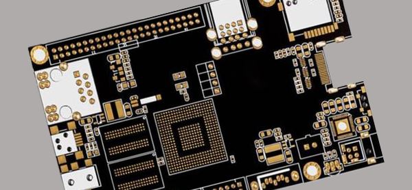
Prototype boards for compact electronics using fine lines, microvias, high-density routing, and controlled fabrication review.
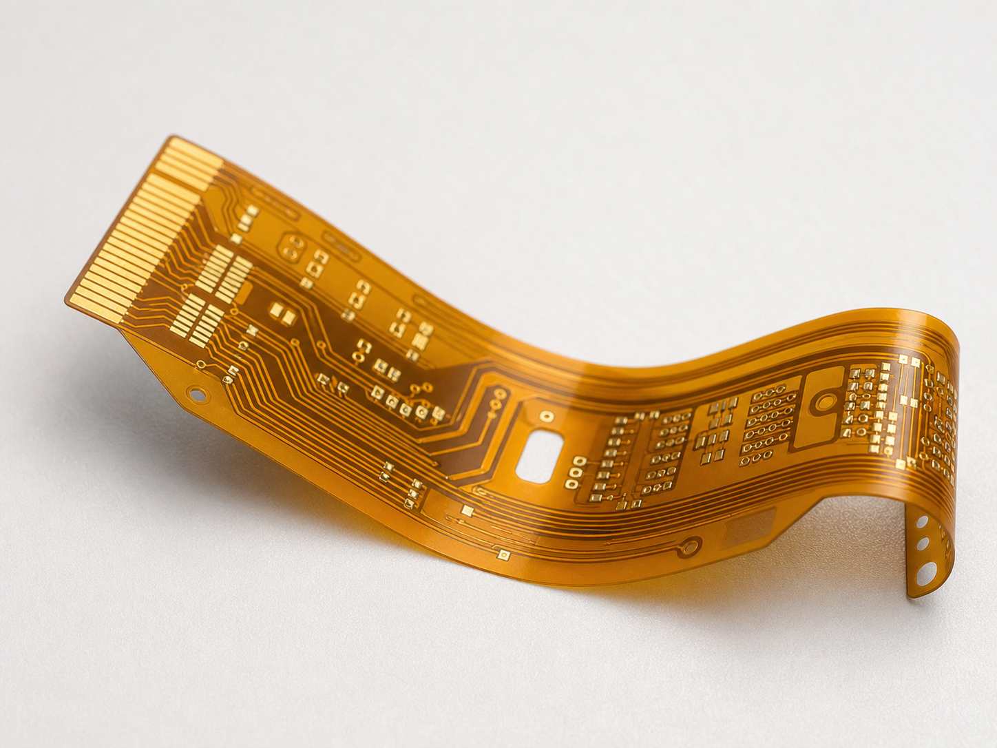
Flexible circuit prototypes for compact, bendable, lightweight, and space-constrained product designs.
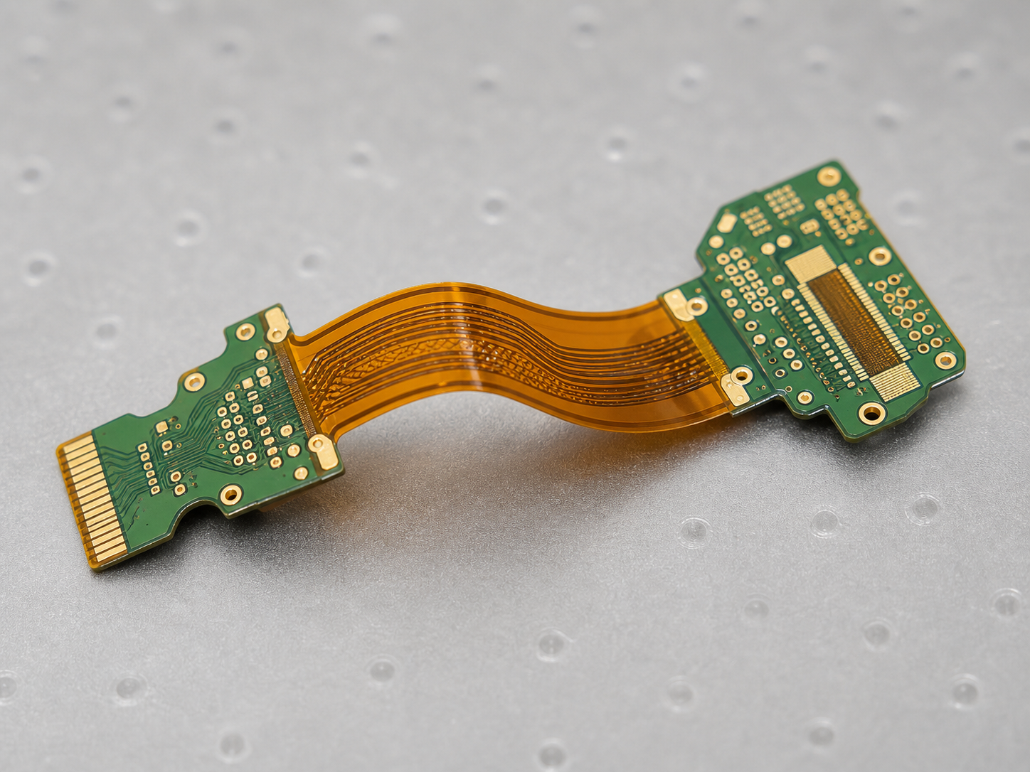
Prototype support for designs that combine rigid board areas with flexible interconnect sections.
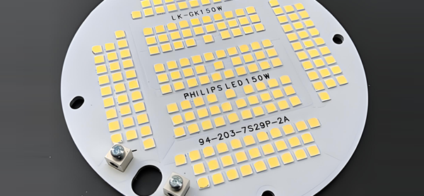
Metal substrate PCB prototypes for thermal testing, LED modules, power electronics, and heat-sensitive applications.
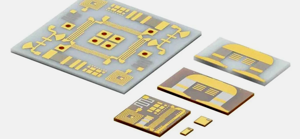
Ceramic substrate prototypes for high thermal conductivity, insulation performance, RF, LED, and high-reliability electronics.
Prototype examples help buyers and engineers compare board structure, material choice, validation purpose, and production path.
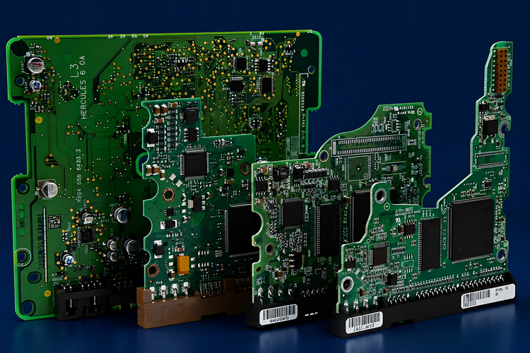
Prototype boards used to validate routing density, connector position, and production readiness before low-volume manufacturing.
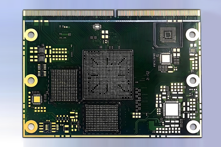
High-density prototype used to verify microvia strategy, fine-pitch routing, and electrical reliability in a compact device.
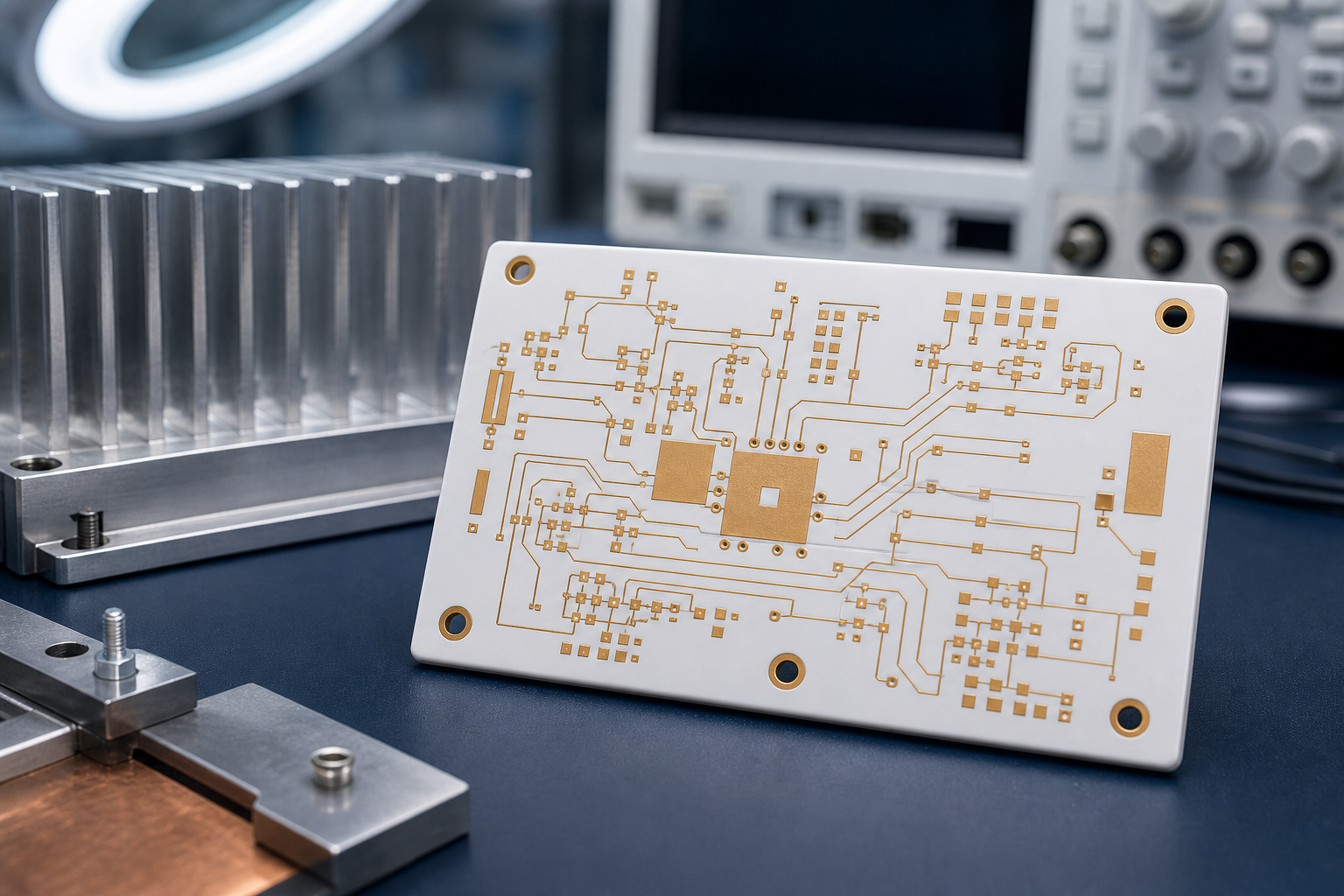
Ceramic substrate prototype used for high thermal conductivity, insulation performance, and demanding reliability evaluation.
We offer a wide range of prototype PCB materials and structures to match different engineering validation needs.
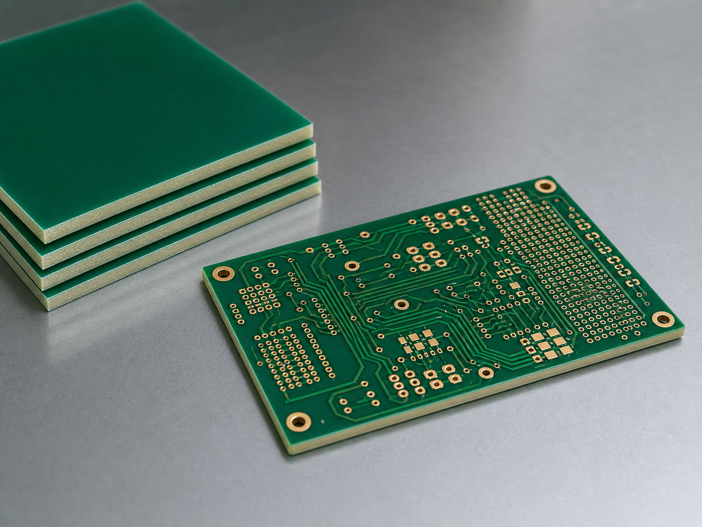
 FR4 PCB Materials
Standard FR4 material options for cost-controlled PCB samples, multilayer stack-up validation, and general engineering tests.
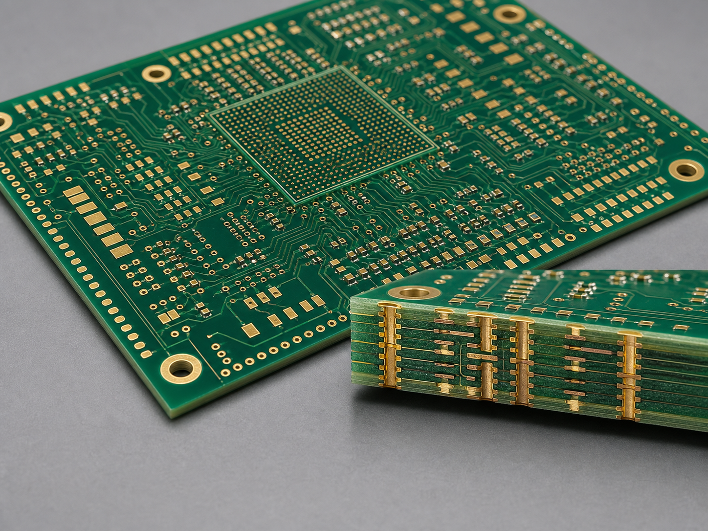 HDI PCB Structure
High-density PCB structure options for microvias, fine lines, compact BGA areas, and advanced routing validation.
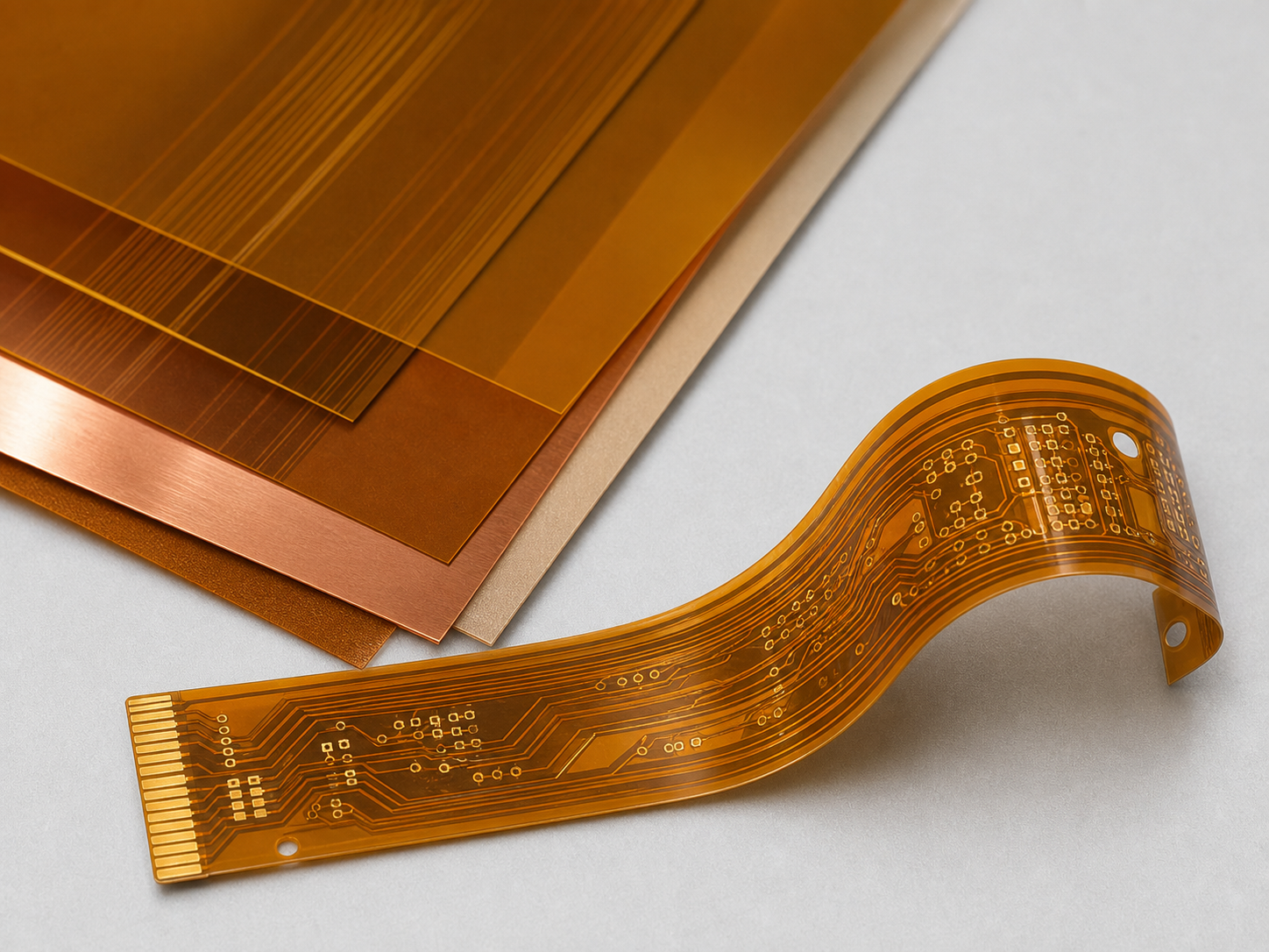 Flexible PCB Materials
Polyimide flexible circuit material options for bendable, lightweight, compact, and space-constrained designs.
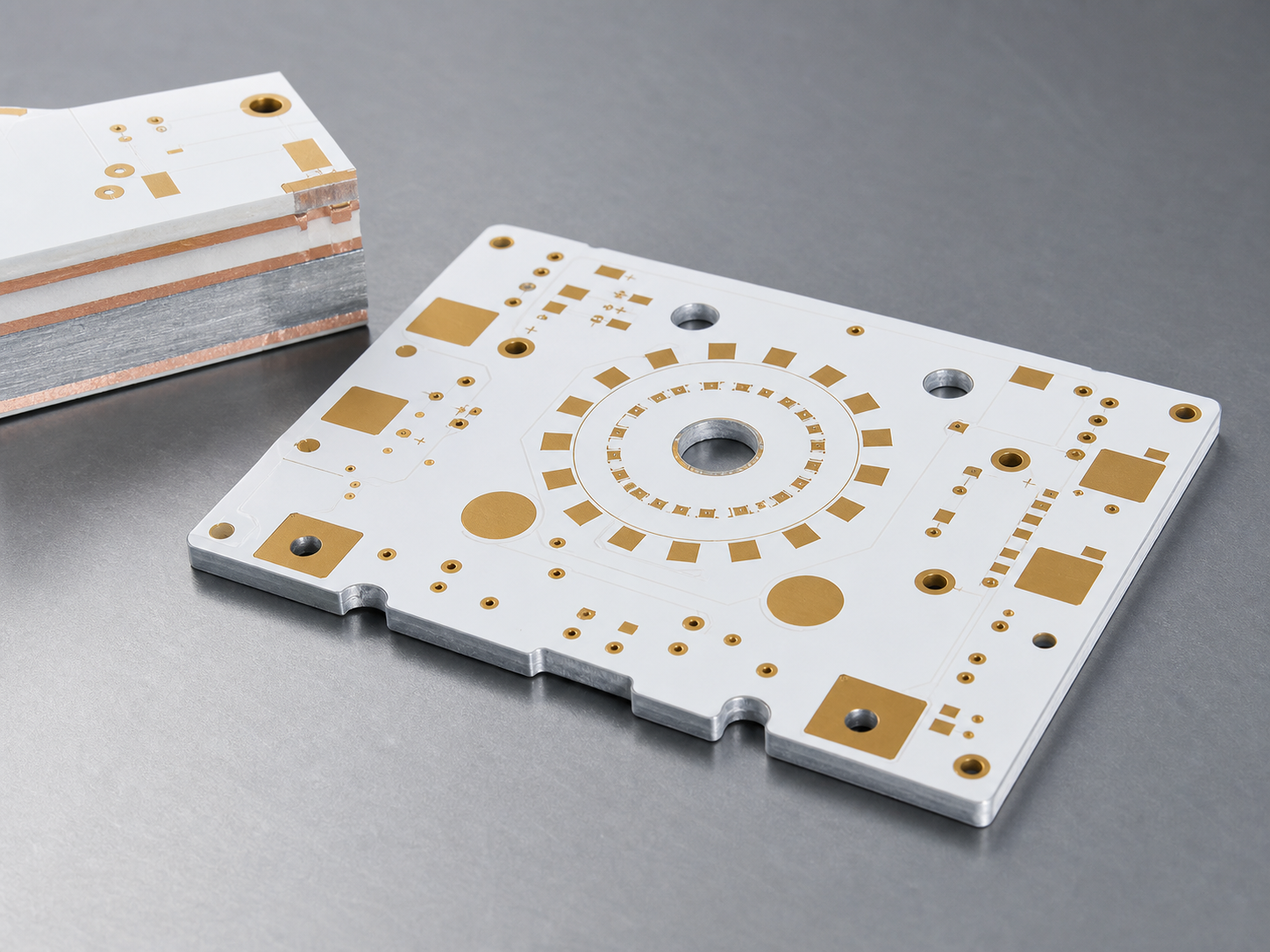 Aluminum PCB Materials
Metal core material options for LED modules, power electronics, thermal design, and heat-sensitive applications.
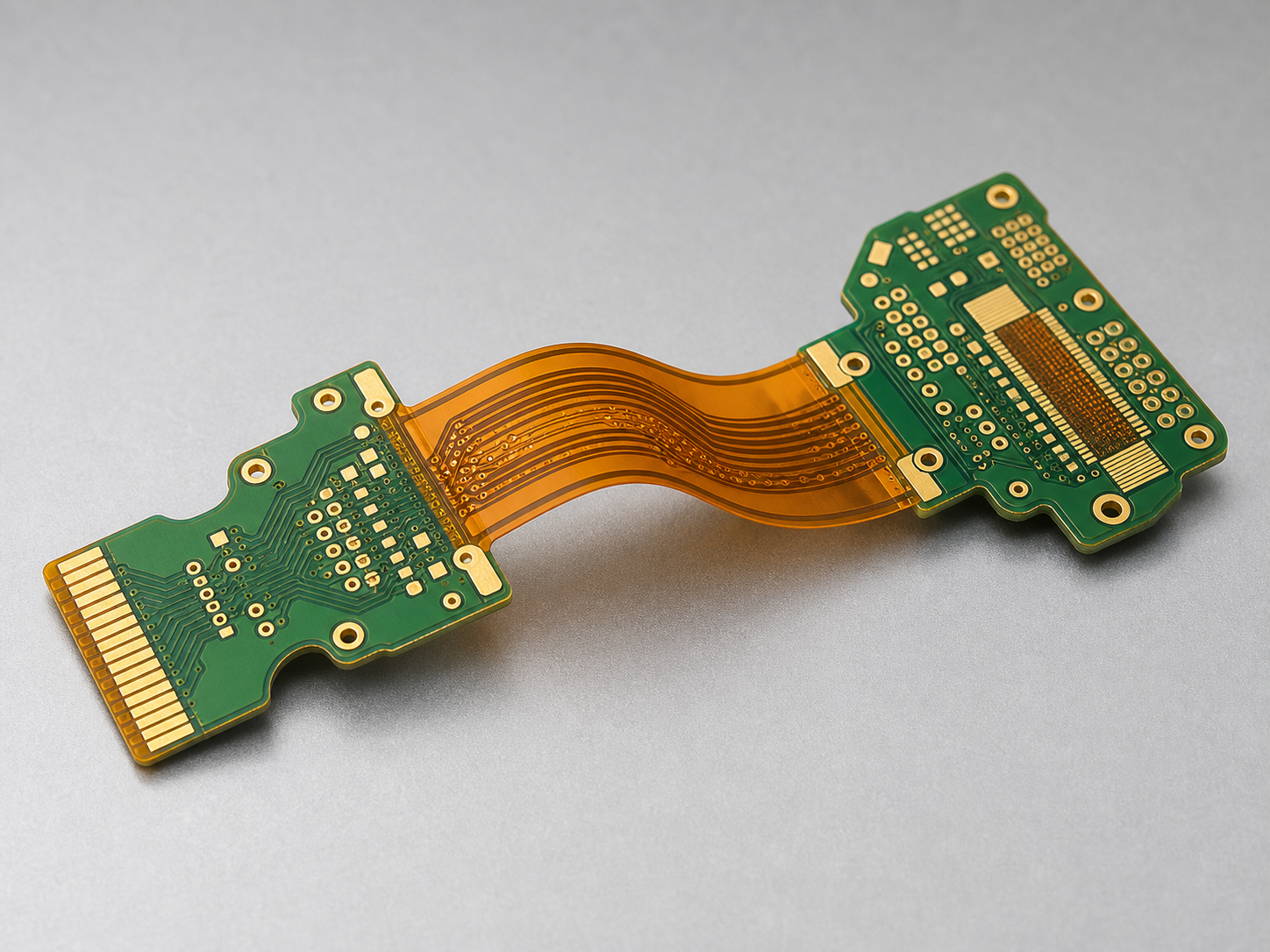 Rigid-Flex PCB Structure
Combined rigid and flexible PCB structure for products that need stable board areas and bendable interconnect sections.
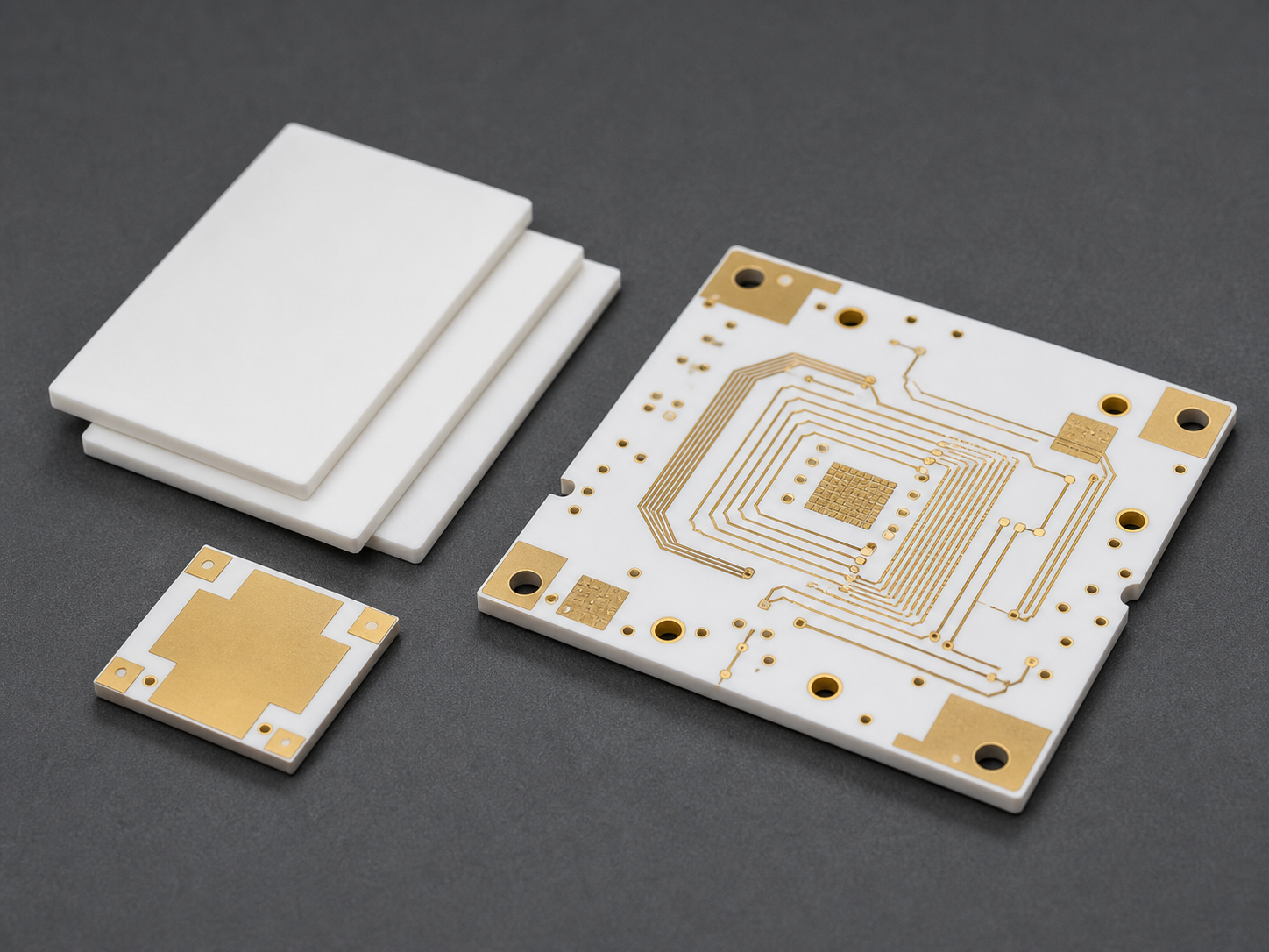 Ceramic PCB Materials
Ceramic substrate material options for thermal conductivity, insulation performance, RF, LED, and high-reliability use.
A clear process helps engineering teams reduce communication time and move from files to confirmed prototype production with less risk.
Prototype quality matters because one sample can decide design release, test schedule, and future production confidence. EBest Circuit focuses on stable fabrication control and clear engineering communication.
A DEDICATED ENGINEERING TEAM FOR EVERY CUSTOMER
You work with a dedicated engineering team, not just a salesperson. From prototype to production, we help solve problems and keep your project moving.
More Than a Supplier. Your Engineering Partner.
01
We review your files before production to reduce mistakes and delays.
02
If a component is unavailable, we help find a suitable alternative.
03
We keep your approved BOM and project details for future builds.
04
PCB, sourcing, assembly, testing and quality are managed together.
FROM PROTOTYPE TO PRODUCTION
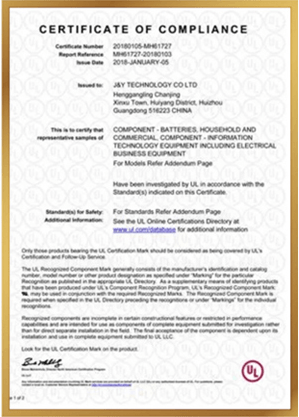
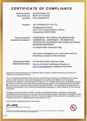
Are you worried about quality certification? We support relevant quality certifications and RoHS-compliant quality management communication to help overseas buyers reduce supplier risk.
Clear prototype requirements help engineering sales review price, lead time, material choice, test needs, and production risk more accurately.
Upload Gerber for QuoteAnswers for engineers and buyers evaluating PCB prototype manufacturing, quick-turn needs, advanced board types, and prototype-to-production planning.
Related articles for engineers researching PCB prototype manufacturing, fast turnaround options, DFM review, material choices, and advanced prototype boards.
View All Articles
Learn which files, board requirements, material notes, and testing details help manufacturers quote prototype PCB projects accurately.
Read Featured ArticleCompare PCB manufacturing options for New Zealand projects. Check local versus overseas supply, RFQ files, landed cost, DFM, quality evidence and delivery risk.
Read MoreCompare prototype PCB manufacture UK options by DFM response, PCB/PCBA scope, certificates, quote clarity, lead-time planning and RFQ readiness.
Read MoreCompare California PCB prototype manufacturer options by file review, DFM response, PCBA scope, certificates, service type and quote clarity.
Read MorePCB prototype service for rigid, HDI, RF, heavy copper, metal-core, ceramic, flex, rigid-flex, and turnkey PCBA projects with DFM review.
Read MoreLearn quick turn PCB lead times, quote files, manufacturing, assembly, quality controls, cost drivers and supplier checks.
Read MoreCompare quick turn PCB manufacturers by DFM review, files, lead-time risk, prototype needs, assembly scope, testing and RFQ checklist.
Read More