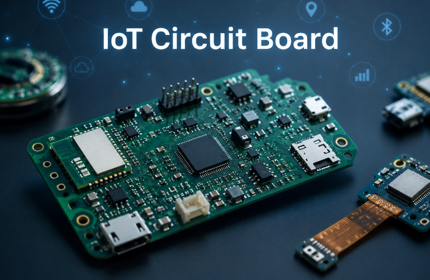
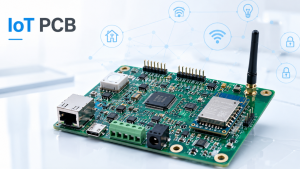
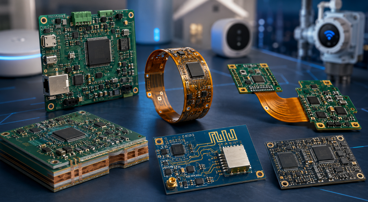
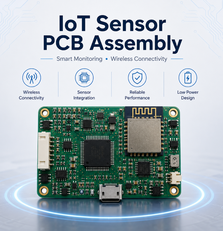
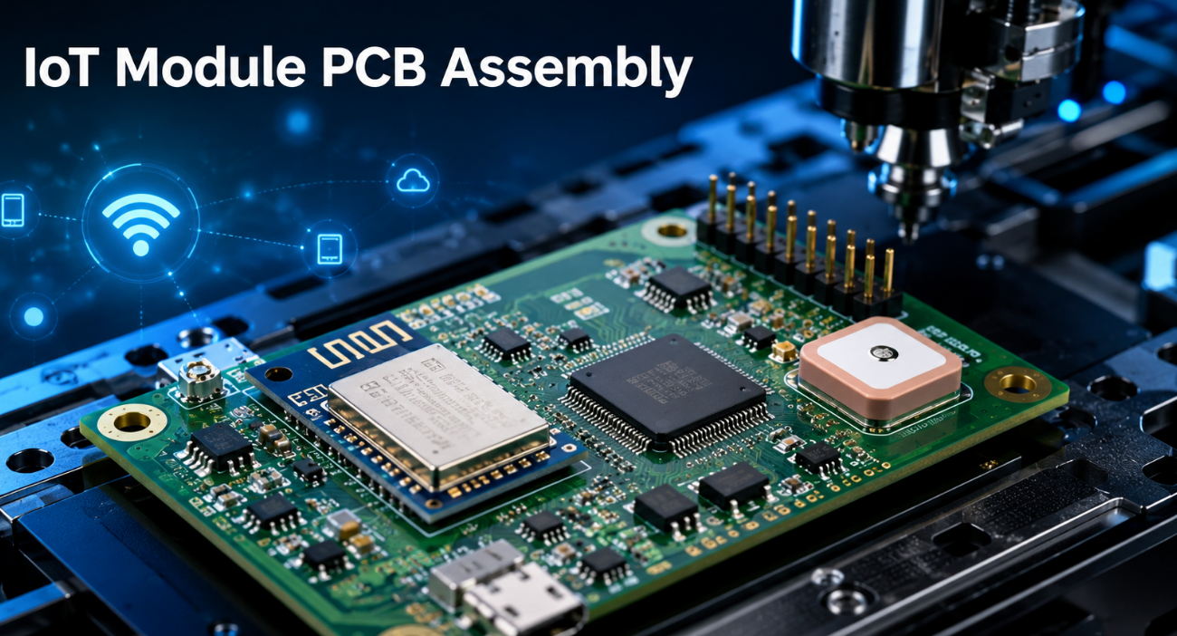
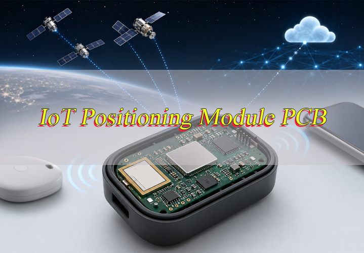
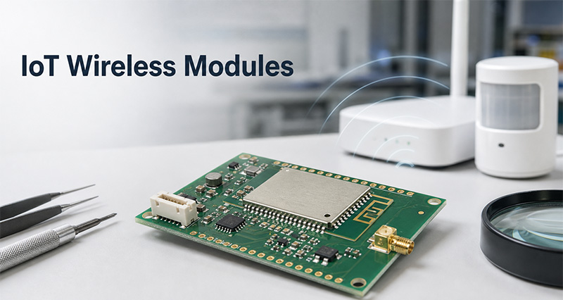
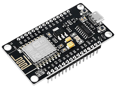
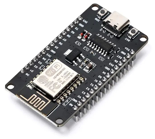
Internet of things wireless modules help connected products send and receive data through Wi-Fi, Bluetooth, LoRa, Zigbee, NB-IoT, LTE-M, cellular, or other wireless technologies. They are widely used in smart sensors, industrial monitoring devices, medical electronics, asset trackers, smart meters, gateways, wearable devices, and compact control systems.
For engineers, the wireless module itself is only one part of the product. The final performance also depends on the PCB, antenna area, power supply, connector reliability, SMT assembly, cleaning, testing, and production control. EBest Circuit (Best Technology) supports PCB manufacturing, DFM review, component sourcing based on approved BOM, PCBA assembly, inspection, and testing for IoT wireless module projects. If you are preparing an IoT PCB or IoT module PCB assembly project, send your Gerber files, ODB++ files, BOM, drawings, assembly notes, or testing requirements to sales@bestpcbs.com for engineering review before production.
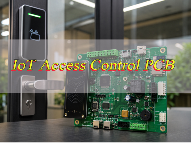
What Are Internet of Things Wireless Modules?
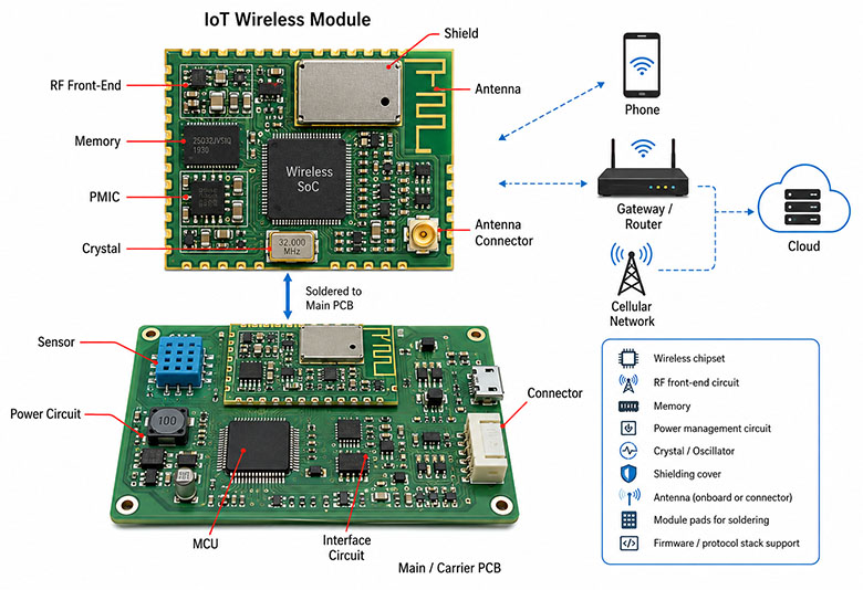
Internet of things wireless modules are compact electronic modules that give a device wireless communication capability. Instead of building the full radio circuit from the beginning, many engineers use a ready-made wireless module that already includes key communication parts.
A typical IoT wireless module may include:
- Wireless chipset
- RF front-end circuit
- Memory
- Power management circuit
- Crystal or oscillator
- Shielding cover
- Antenna connector or onboard antenna
- Module pads for soldering to the main PCB
- Firmware or communication stack support from the module supplier
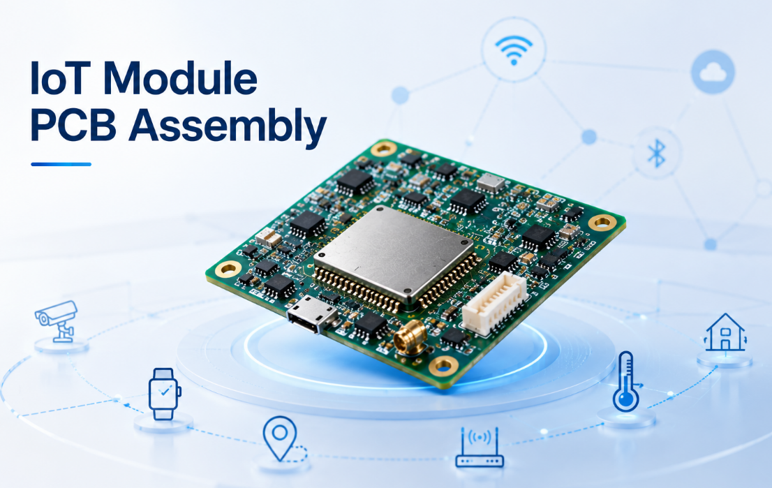
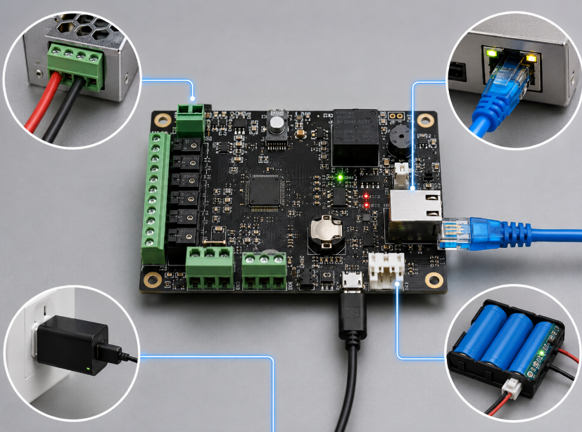
The module allows the end product to connect to nearby devices, a gateway, a router, a cellular network, or a cloud platform. In a real product, the module usually sits on a carrier PCB or main control board with sensors, connectors, power circuits, MCU, interface circuits, and mechanical mounting features.
How Do IoT Wireless Modules Connect Devices?
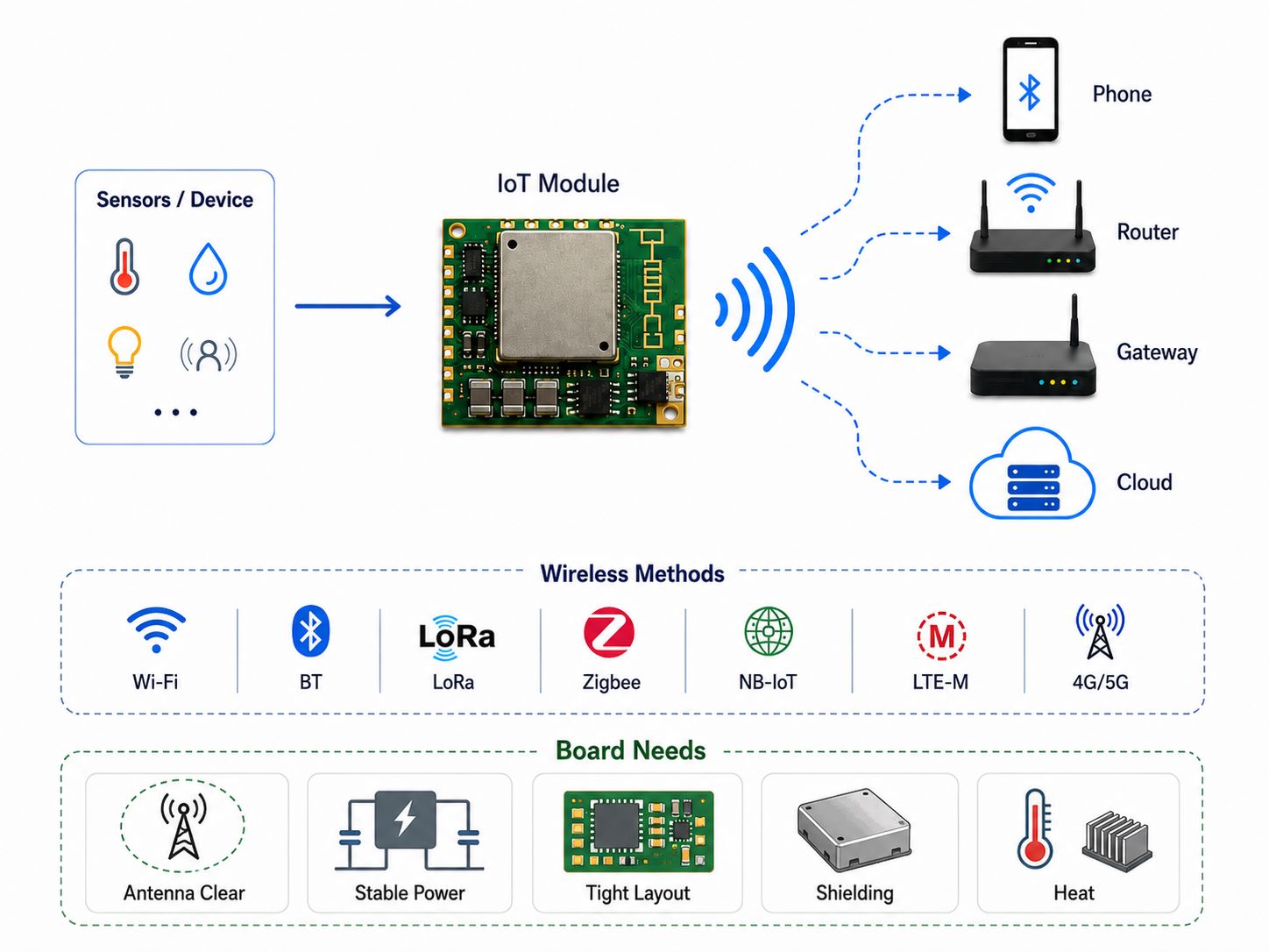
IoT wireless modules connect devices by converting sensor, control, or system data into wireless signals. The module communicates with other devices, a local network, or a remote server depending on the selected wireless technology.
For example:
| Wireless Method | Common Use |
|---|---|
| Wi-Fi | High data rate, local internet access |
| Bluetooth | Short-range device connection |
| LoRa | Long-range, low-power sensing |
| Zigbee | Mesh networks and smart devices |
| NB-IoT | Low-power cellular IoT |
| LTE-M | Mobile IoT with better data support |
| 4G/5G cellular | Wide-area data connection |
For PCB and PCBA manufacturing, the important point is that different wireless technologies create different board-level requirements. A Wi-Fi module may need careful antenna clearance. A cellular IoT module may need stronger power stability. A compact wearable product may need tight component placement and controlled mechanical size. A gateway may need connectors, shielding, thermal control, and reliable assembly.
Common Types of Wireless Modules for IoT Products
Wireless modules for IoT products are usually selected by the customer’s engineering team according to communication distance, data rate, power consumption, certification requirements, network availability, and product cost.
Common types include:
Wi-Fi modules
Used when the product needs local network access, higher data rate, and internet connectivity through routers or access points.
Bluetooth modules
Used for short-range communication, mobile app connection, wearable devices, handheld devices, and low-power accessories.
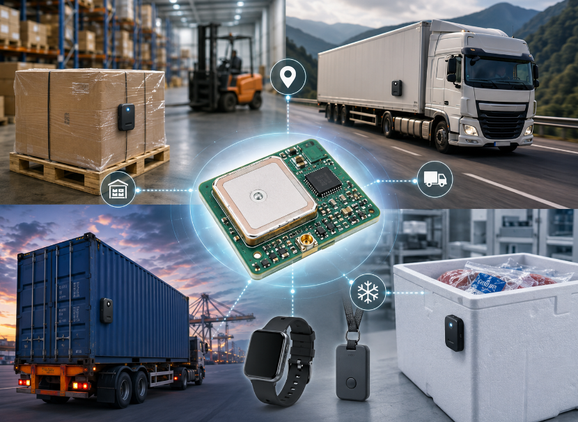
LoRa modules
Used for long-range, low-power sensing applications such as smart agriculture, metering, environmental monitoring, and remote sensors.
Zigbee modules
Used for mesh networks, smart home devices, building automation, lighting control, and low-power device networks.
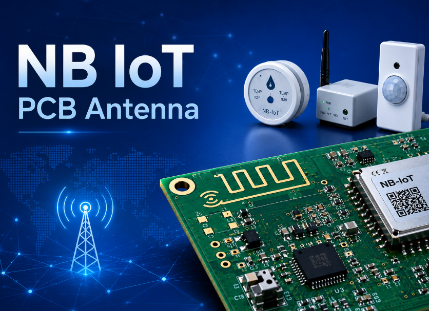
NB-IoT and LTE-M modules
Used for low-power cellular IoT products that need wide-area coverage, such as smart meters, trackers, and industrial monitoring devices.
Cellular modules
Used for devices that need mobile network connectivity, higher coverage, or remote data transmission without relying on local Wi-Fi.
EBest Circuit does not need to choose the wireless protocol for the customer. Our role is to manufacture and assemble the PCB or PCBA according to the customer-approved design files, BOM, module selection, and production requirements.
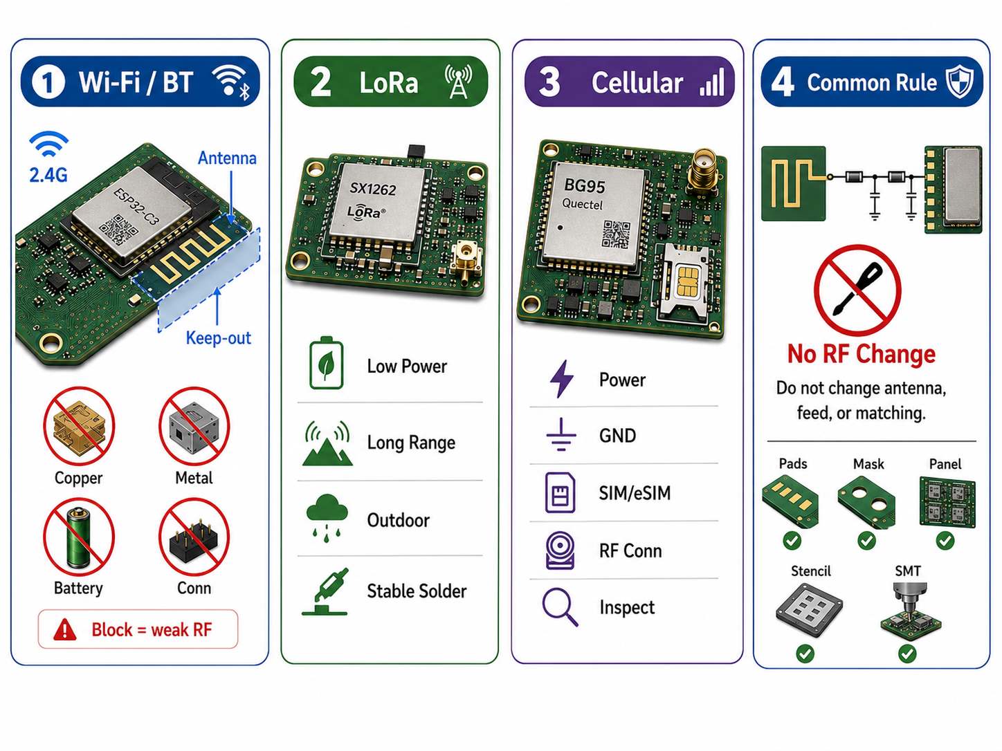
Wi-Fi, Bluetooth, LoRa, and Cellular IoT Modules
Each IoT module type has different PCB manufacturing and assembly concerns.
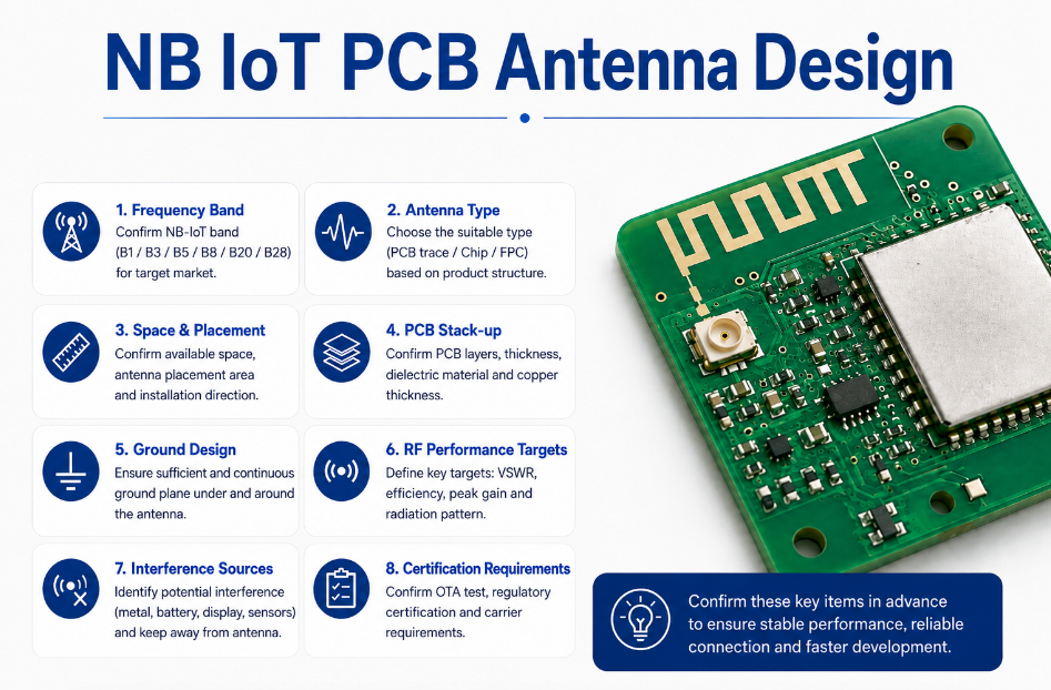
Wi-Fi and Bluetooth modules often operate in the 2.4GHz band, so antenna position and keep-out areas matter. If the antenna area is blocked by copper, metal housing, battery, connector, or enclosure structure, wireless performance may be affected.
LoRa modules are often used in low-power, long-range products. These projects may care more about battery life, stable solder joints, connector reliability, and outdoor or industrial operating conditions.
Cellular IoT modules may require stronger power handling, good grounding, reliable SIM/eSIM related areas, antenna connector assembly, and careful inspection after SMT. Power peaks, vibration, and connector contact can matter more in field-deployed products.
For all these modules, the PCB manufacturer should not change RF layout, antenna geometry, or matching circuits without customer approval. However, the manufacturer should review manufacturability risks such as pad design, solder mask opening, panelization, stencil, SMT process, connector placement, and inspection points.
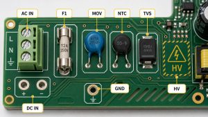
Internet of Things Wireless Modules PCB Requirements
Internet of things wireless modules place several practical requirements on PCB manufacturing.
The PCB must support the module footprint accurately. If the pad size, solder mask opening, stencil design, or assembly process is not suitable, the module may shift, tombstone nearby components, bridge, or form weak solder joints.
Important PCB requirements include:
| PCB Area | What to Check |
|---|---|
| Module footprint | Pad size and solderability |
| Antenna zone | Keep-out and copper clearance |
| Power path | Stable supply and copper width |
| Grounding | Clean return path and shielding support |
| Connectors | Mechanical strength and alignment |
| Surface finish | ENIG or suitable solderable finish |
| Panelization | SMT efficiency and board protection |
| Test points | Easier inspection and testing |
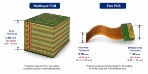
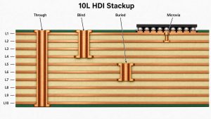
For high-density IoT products, the PCB may also require HDI, blind vias, fine line/space, impedance review, rigid-flex construction, or special thickness control. These points should be confirmed before production starts.
IoT Module PCB Layout and Manufacturing Checks
IoT module PCB layout should be reviewed from a manufacturing and assembly point of view before the board enters production. This does not mean changing the customer’s circuit design. It means checking whether the provided files can be manufactured and assembled reliably.
Key checks include:
- Is the wireless module footprint correct?
- Are module pads suitable for SMT assembly?
- Is the antenna keep-out area clearly defined?
- Are large copper areas balanced enough for soldering?
- Are vias too close to module pads or connectors?
- Are test points accessible?
- Is the board shape suitable for panelization?
- Are castellated holes, edge connectors, or antenna connectors manufacturable?
- Does the drawing match the Gerber and BOM?
- Are special notes clear before production?
For IoT wireless module products, many issues are not caused by the wireless module itself. They come from small manufacturing details: poor solder paste control, unclear assembly notes, tight connector spacing, weak panel support, insufficient test access, or missing inspection requirements.
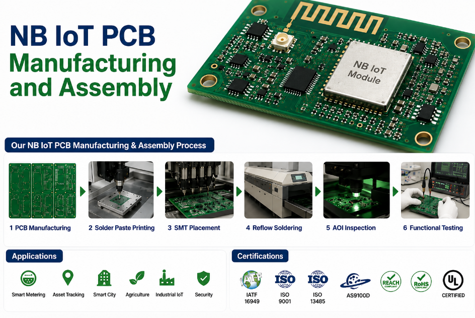
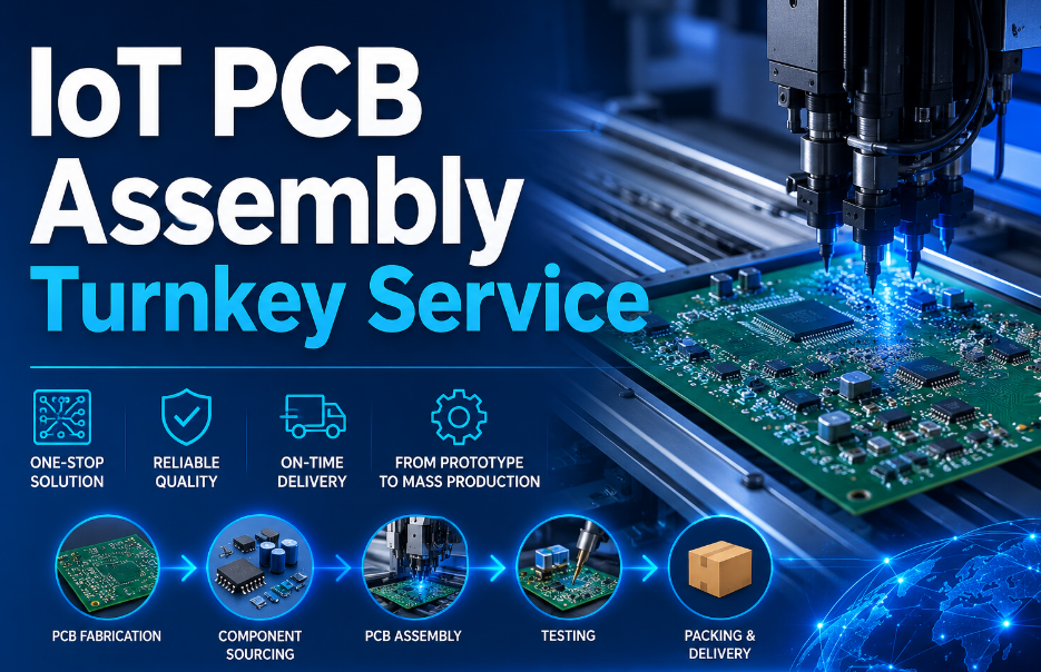
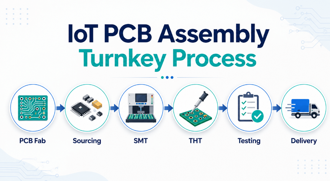
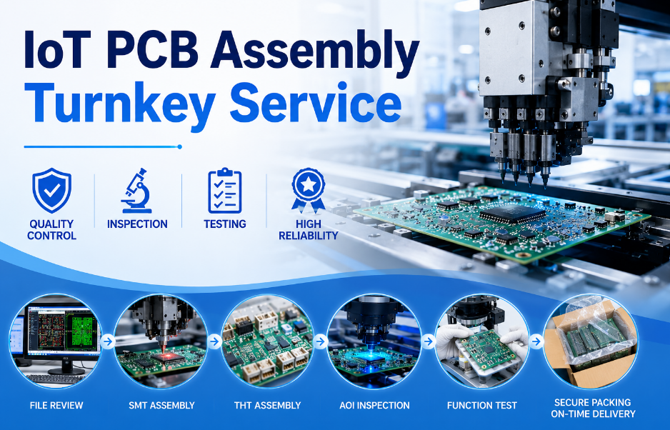
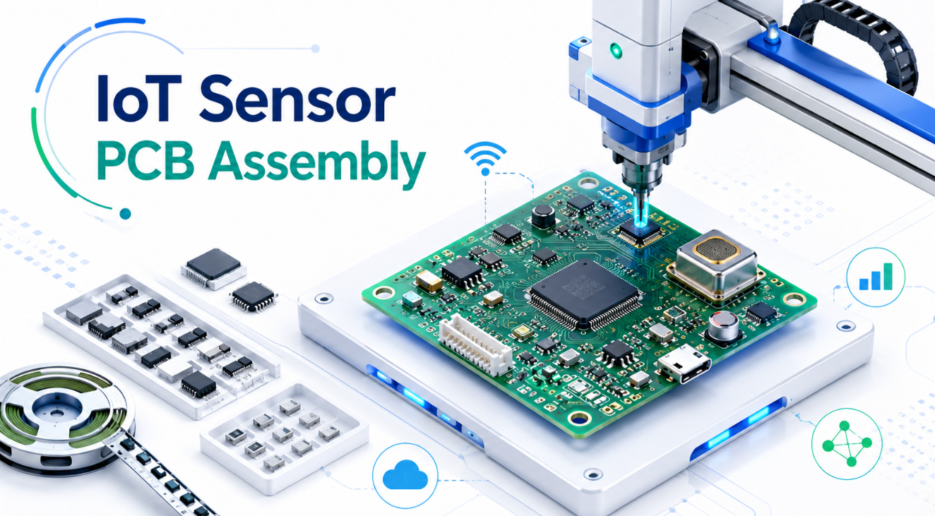
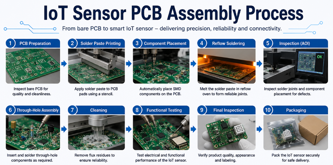
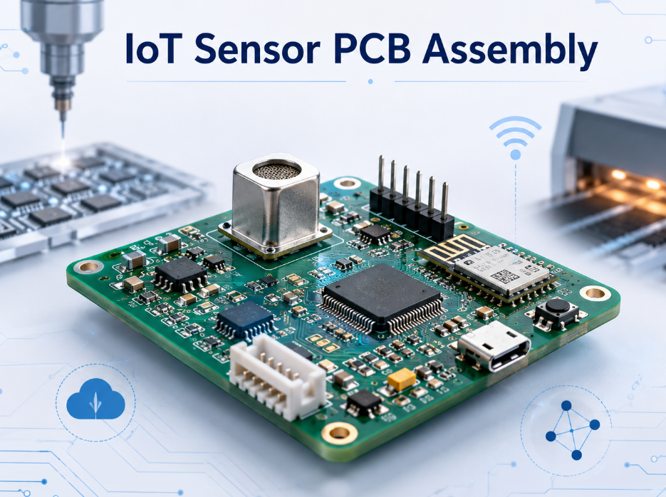
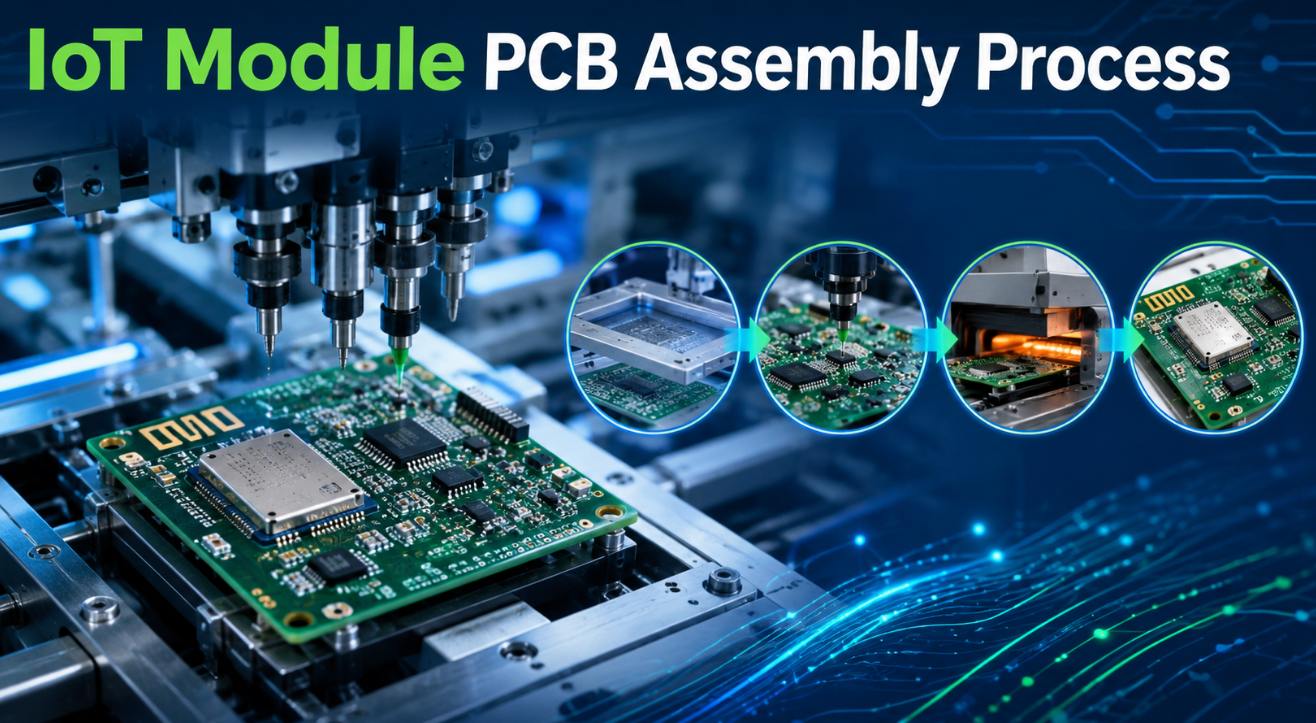
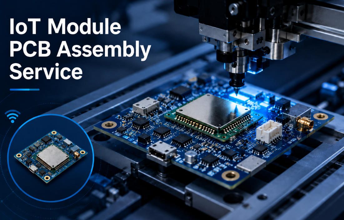
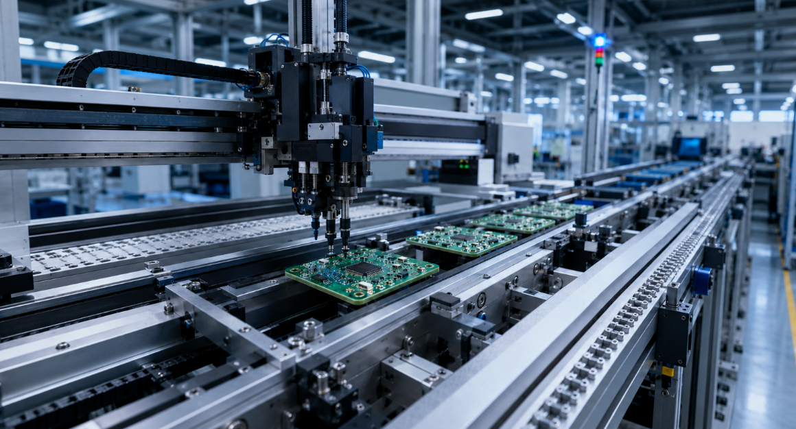
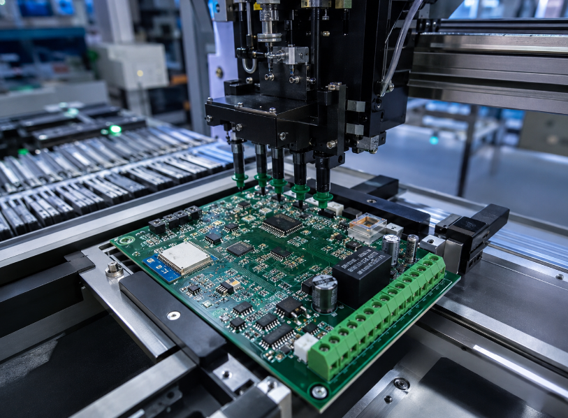
PCBA Assembly for IoT Wireless Modules
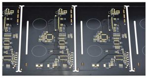
PCBA assembly is a key part of IoT wireless module production. Wireless modules may be shielded, relatively large, heat-sensitive, or sensitive to solder paste volume. Some products also include fine passive components, sensors, connectors, LEDs, buttons, battery holders, SIM card holders, or antenna connectors on the same board.
During IoT wireless module PCBA assembly, EBest Circuit can support:
- Component sourcing based on approved BOM
- SMT assembly
- Connector assembly
- Solder paste and stencil review
- Module placement inspection
- AOI inspection
- X-ray inspection when required
- Functional testing coordination
- Cleaning and packing requirements
- Prototype and small-batch production
The most important point is process visibility. The module, PCB, BOM, SMT, testing, and packing requirements should be handled as one project, not as separate disconnected steps.
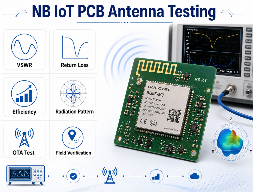
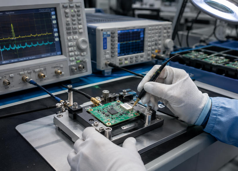
Testing and Reliability for IoT Wireless Module Products
IoT wireless module products are often used in real environments, not only on a lab bench. They may be installed inside industrial equipment, medical devices, smart meters, outdoor sensors, gateways, access control devices, or portable products.
Reliability checks may include:
| Reliability Area | Typical Concern |
|---|---|
| Solder joints | Module and connector strength |
| Power stability | Stable module operation |
| RF area | No unwanted copper or obstruction |
| Cleanliness | No residue near fine components |
| Connectors | Contact and insertion reliability |
| Environment | Heat, humidity, vibration, enclosure fit |
| Traceability | Production and batch records |
Some testing is defined by the customer, such as functional testing, communication testing, programming, current measurement, LED status check, or connector inspection. EBest Circuit can coordinate PCBA testing according to the customer’s approved test method and production requirements.
IoT Wireless Module PCB Manufacturing Case Study
A European industrial customer needed a 6-layer FR4 PCB for an IoT wireless monitoring product used in equipment data collection. The wireless module and circuit design were already defined by the customer. EBest Circuit’s role was to review the manufacturing files, confirm the production stackup, control the impedance-related requirements, and fabricate the PCB according to the approved documents.
Project requirements
- 6-layer FR4 PCB
- IT180 material, with Isola 370HR or equivalent material required
- Outer copper: 1oz
- Inner copper: 0.5oz
- Board thickness: 1.6mm ±10%
- Surface finish: ENIG, Au 1u”
- Green solder mask, white silkscreen
- Differential impedance requirement according to the customer’s PDF specification
- Bare PCB delivery
- Factory panelization allowed
- Production files had to be sent to the customer for confirmation before manufacturing
Why this project needed careful review
This was not a simple FR4 board order. For an IoT wireless module product, the PCB had to support stable signal transmission, reliable assembly, and predictable production quality.
The first checkpoint was the material. The customer specified IT180 and allowed Isola 370HR or equivalent material, so the material choice had to be confirmed before production.
The second checkpoint was impedance. Because the customer required differential impedance, EBest Circuit had to review the stackup, copper thickness, dielectric structure, and impedance notes in the customer’s PDF specification before fabrication.
The third checkpoint was documentation. The customer required production files to be confirmed before manufacturing. This helped make sure the stackup, material, copper thickness, surface finish, panelization, and impedance requirements were aligned before the board entered production.
EBest Circuit’s manufacturing support
- Reviewed Gerber files, drawing, and customer PDF specification
- Prepared production stackup and production files for customer confirmation
- Checked material requirement: IT180 / Isola 370HR equivalent
- Reviewed differential impedance requirements before fabrication
- Confirmed copper thickness, board thickness, ENIG, solder mask, and silkscreen
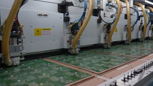
- Arranged factory panelization for bare PCB production
- Controlled the project according to the approved production documents
For the customer, the value was not only receiving a 6-layer PCB. The important value was that the manufacturing details were reviewed before production started. Material, impedance, stackup, copper thickness, finish, and panelization were confirmed first, helping reduce risk for the IoT wireless module product before assembly and system validation.
Why Choose EBest Circuit for IoT Wireless Module PCB and PCBA?
EBest Circuit is suitable for customers who need PCB and PCBA manufacturing support for IoT wireless module products, especially when the project needs more than bare PCB fabrication.
Customers choose EBest Circuit because we can support:
- PCB fabrication
- Component sourcing based on approved BOM
- SMT assembly
- Connector assembly
- DFM review before production
- BOM optimization suggestions
- Prototype and small-batch support
- PCBA inspection and testing coordination
- One-stop PCB + sourcing + IoT PCB assembly turnkey service
- ISO9001, ISO13485, IATF16949, and AS9100D quality systems
- Digital workshop traceability
For IoT wireless modules, this one-stop support is useful because many production risks happen between steps. A footprint issue, BOM substitution, connector mismatch, antenna clearance mistake, or unclear test note can affect the final product. EBest Circuit helps keep these details visible from engineering review to shipment.
If you are building an IoT wireless module product, send your Gerber files, ODB++ files, BOM, drawings, module datasheet, assembly notes, testing method, or packing requirements to sales@bestpcbs.com. Our engineering team can help review the PCB and PCBA manufacturing path before production starts.
FAQs about Internet of Things Wireless Modules
1. What are internet of things wireless modules?
Internet of things wireless modules are compact communication modules that help devices connect through Wi-Fi, Bluetooth, LoRa, Zigbee, NB-IoT, LTE-M, cellular, or other wireless technologies.
2. What is the difference between IoT modules and wireless modules?
A wireless module provides communication capability. An IoT module is usually a wireless module used inside a connected product, often with sensors, power circuits, MCU, firmware, and cloud or gateway communication.
3. Can EBest Circuit design the wireless module circuit?
EBest Circuit mainly supports PCB manufacturing, DFM review, component sourcing based on approved BOM, PCBA assembly, inspection, and testing coordination. We manufacture and assemble according to customer-approved design files, BOM, and production requirements.
4. What should I prepare for an IoT wireless module PCBA project?
You should prepare Gerber or ODB++ files, BOM, placement file, drawings, module datasheet, assembly notes, testing instructions, firmware or programming notes if needed, and packing requirements.
5. Why is PCB manufacturing important for IoT wireless modules?
The PCB affects module soldering, antenna area, power stability, connector reliability, test access, mechanical fit, and production yield. A good manufacturing review helps reduce risk before SMT assembly.
Need help with an IoT wireless module PCB or PCBA project? Pls feel free to send your Gerber files, ODB++ files, BOM, module datasheet, drawings, assembly notes, or test requirements to sales@bestpcbs.com. EBest Circuit’s engineering team can help review the PCB and PCBA manufacturing path before production starts.