PCB manufacturing PCB manufacturing
Home > Blog

SMT stencil

Precision Solder Paste Stencil for Reliable SMT PCB Assembly
Wednesday, June 24th, 2026

A solder paste stencil is one of the first process tools used in SMT PCB assembly, but it has a direct impact on final soldering quality. It controls solder paste volume, pad coverage, paste release, and solder joint consistency after reflow. A well-designed stencil helps reduce common SMT defects such as solder bridging, insufficient solder, tombstoning, solder balls, BGA open joints, and excessive voiding under exposed pads.

EBest Circuit supports SMT stencil and PCB assembly projects with laser-cut stencils, etched stencils, framed and frameless options, electro-polished apertures, fiducial marks, step-up/down technology, and BGA ball mounting stencils. Our team can review Gerber files, paste layers, BOM, Pick-and-Place files, and assembly requirements before production to help improve solder paste printing stability. For solder paste stencil support or full and partial turnkey PCB assembly, please send your files and requirements to sales@bestpcbs.com.

solder paste stencil

What Is a Solder Paste Stencil?

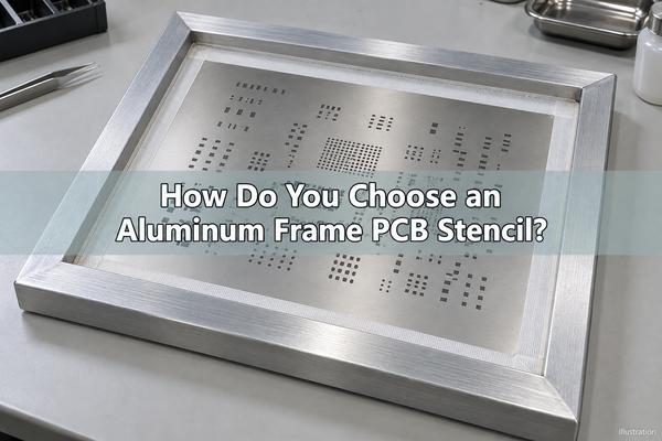
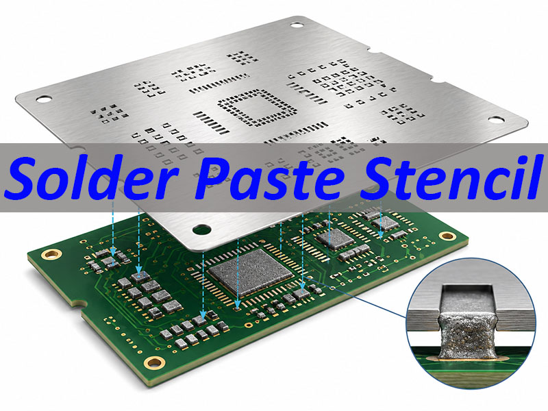
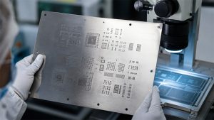
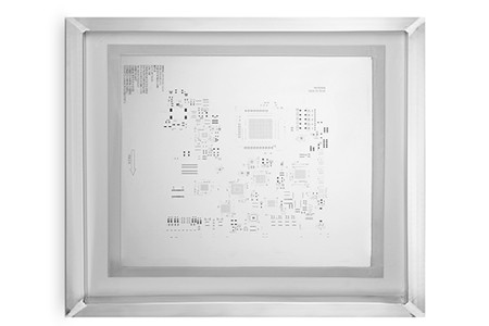
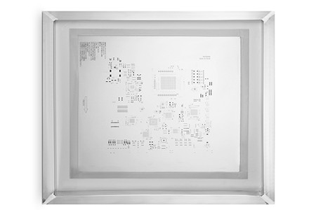
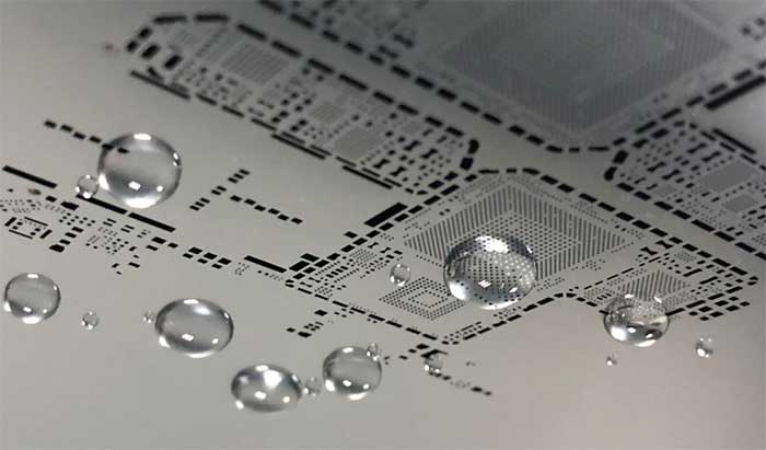
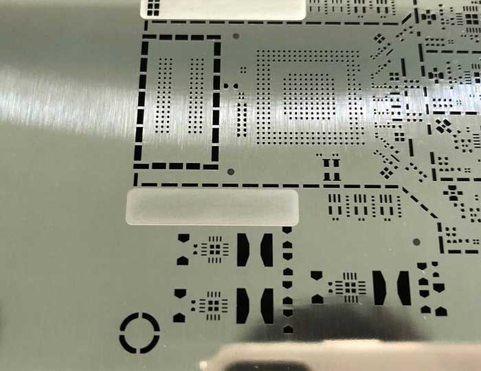
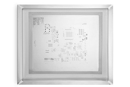
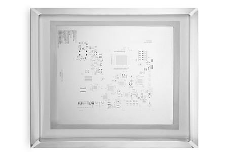
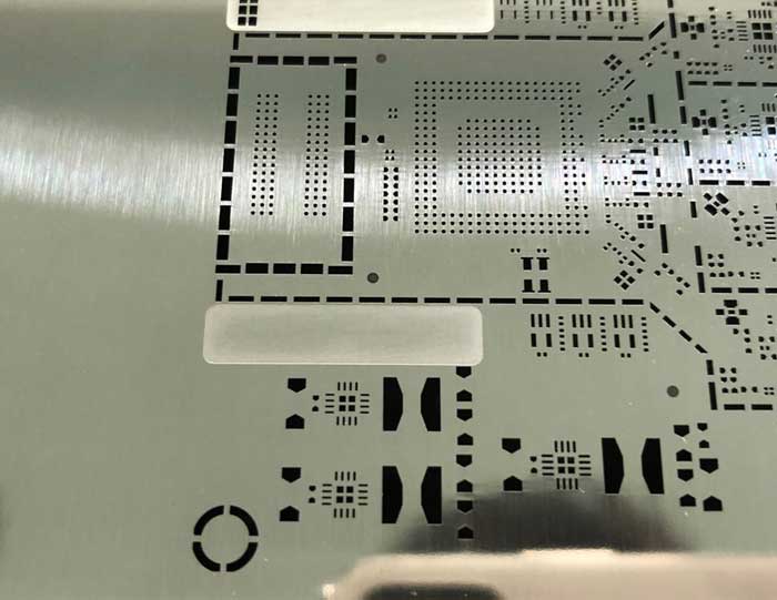
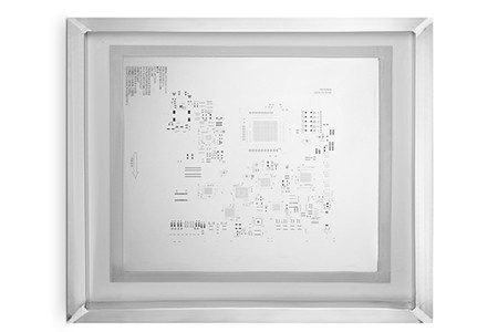
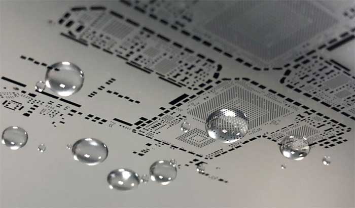
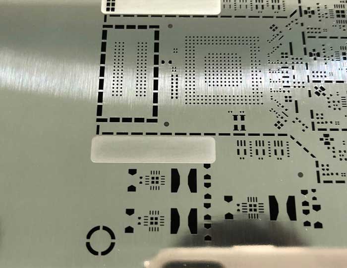
A solder paste stencil is a thin sheet used to print solder paste onto PCB pads before surface mount components are placed. It is usually made from stainless steel and has precise openings called apertures. These apertures match the solder paste layer in the PCB design files.

During printing, the stencil is aligned over the PCB. A squeegee pushes solder paste across the stencil surface. The paste passes through the apertures and lands on the PCB pads. After stencil separation, each pad should have a controlled solder paste deposit.

In simple terms:
A solder paste stencil controls paste volume, paste location, and printing consistency in SMT assembly.

A stencil affects:

  • Solder joint volume
  • Paste printing accuracy
  • Fine-pitch component quality
  • BGA and QFN soldering
  • LED and connector solder strength
  • SMT defect rate
  • PCBA production repeatability

For simple PCB prototypes, a standard stencil may be enough. For fine-pitch ICs, BGA packages, QFN exposed pads, 0201 components, connectors, or LED metal core PCB, stencil design needs a more detailed review.

How Does a Solder Paste Stencil Work in SMT PCB Assembly?

A solder paste stencil is used at the solder paste printing stage. This is one of the earliest and most important steps in SMT assembly. If the paste printing result is unstable, later processes such as placement, reflow, AOI, and X-ray inspection will face more risk.

A typical SMT assembly flow includes:

  • Material and PCB preparation
  • Baking when required
  • Solder paste printing
  • SPI inspection
  • Component placement
  • Reflow soldering
  • AOI inspection
  • X-ray inspection for BGA or hidden joints
  • Functional testing
  • Cleaning and final packaging

The stencil is mainly used during the solder paste printing step. However, its effect can be seen throughout the whole process.

SMT StageStencil Impact
Paste printingControls paste volume
SPIChecks paste quality
PlacementSupports stable mounting
ReflowAffects solder joints
AOIReveals visible defects
X-rayChecks hidden joints

A good stencil helps solder paste transfer cleanly from the aperture to the pad. A poor stencil may leave paste inside the opening, print too much paste, or cause offset deposits.

In production, engineers often check stencil design when defects repeat on the same pads. If the same IC pins keep bridging, or the same QFN center pad has too much solder, the stencil is usually one of the first items to review.

PCB Stencil vs Solder Paste Stencil: Are They the Same?

In most SMT projects, a PCB stencil and a solder paste stencil refer to the same tool. Both are used to print solder paste onto PCB pads.

The difference is mainly in wording.

TermMeaning
Solder paste stencilMost precise term
PCB stencilCommon buyer term
SMT stencilFactory process term
Solder stencilShorter informal term
Circuit board stencilGeneral search term

If you are ordering a stencil for assembly, “solder paste stencil” is the clearest term. It tells the supplier that the stencil is used for SMT solder paste printing, not for marking, coating, or another process.

For accurate stencil production, the supplier usually needs:

  • Gerber files
  • Paste layer
  • PCB outline
  • Fiducial marks
  • BOM
  • Pick-and-Place file
  • Assembly drawing
  • Panel drawing, if applicable

The paste layer is important, but it is not always enough. For better PCBA quality, the stencil should be checked together with component packages and assembly requirements.

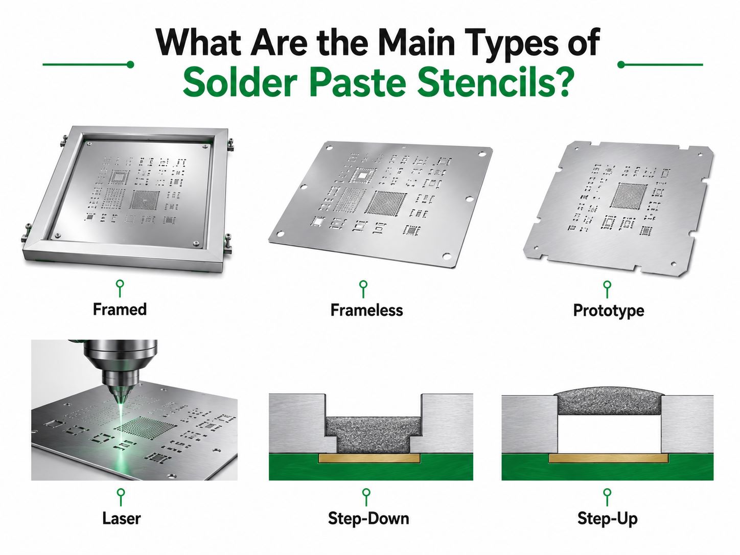
What Are the Main Types of Solder Paste Stencils?

Different PCB assembly projects need different stencil types. A prototype board, a high volume PCB assembly order, and a fine-pitch BGA board may require different stencil choices.

Stencil TypeBest ForKey Value
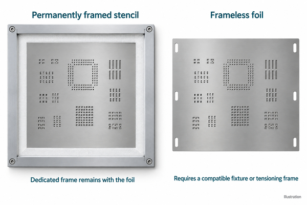
Framed stencilMass productionStable printing
Frameless stencilLow-volume ordersFlexible use
Prototype stencilSamplesFast setup
Laser stencilFine-pitch SMTHigh accuracy
Etched stencilGeneral useCost control
Step-down stencilMixed componentsLocal paste control
Step-up stencilLarge padsExtra paste volume
BGA ball mounting stencilBGA repair or mountingBall placement
PE stencilSpecial applicationsLightweight option

Most SMT stencils today are laser cut because laser cutting offers better aperture accuracy and smoother geometry. Etched stencils are still available for some cost-sensitive or less complex applications.

For higher precision, laser cut stencils may also be electro-polished. Electro-polishing helps smooth the aperture wall and supports better solder paste release. This is especially useful for fine-pitch ICs, QFN pads, small chip components, and dense layouts.

solder paste stencil

How to Choose the Right Solder Paste Stencil Thickness?

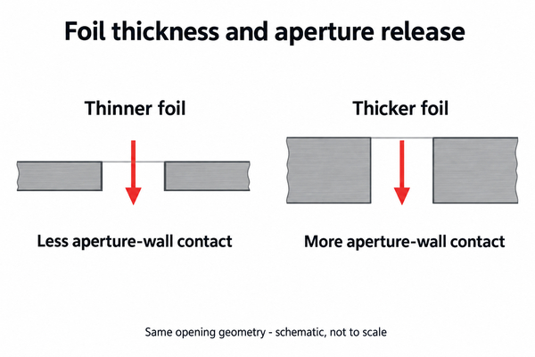
Stencil thickness controls solder paste volume. A thicker stencil prints more paste. A thinner stencil prints less paste. Choosing the right thickness is one of the most important decisions in stencil design.

Common stencil thicknesses include:

ThicknessTypical Use
0.06 mmVery fine features
0.08 mmMiniature SMT
0.10 mmFine-pitch ICs
0.12 mmStandard SMT
0.15 mmGeneral components
0.20 mmLarger pads
Up to 0.60 mmSpecial process

For most PCB assembly projects, 0.10 mm, 0.12 mm, and 0.15 mm are commonly used. The final choice depends on the smallest component, pad pitch, solder paste type, and required solder volume.

Component TypeSuggested ThicknessReason
02010.08–0.10 mmLess paste
04020.10–0.12 mmStable print
0603 / 08050.12–0.15 mmStandard volume
Fine-pitch IC0.10–0.12 mmLess bridging
QFN / DFN0.10–0.12 mmBetter control
BGA0.10–0.12 mmEven deposits
Connectors0.15 mm+More solder
LED pads0.12–0.15 mmHeat and strength
Mixed layoutStep stencilLocal control

A common problem is mixed component size. One PCB may include a fine-pitch IC and a large connector on the same side. If the whole stencil is too thick, the IC may bridge. If it is too thin, the connector may receive insufficient solder.

There are three common solutions:

  • Reduce apertures in fine-pitch areas
  • Use window-pane design on large pads
  • Use step-up or step-down stencil technology

A good stencil choice should start from the most sensitive component, then adjust aperture design for larger pads.

How Does Aperture Design Affect Solder Paste Printing?

Apertures are the openings in the stencil. They decide where solder paste goes and how much paste reaches the pad.

Stencil thickness controls paste height. Aperture design controls paste area and release behavior. Both must work together.

Important aperture design factors include:

  • Aperture size
  • Aperture shape
  • Opening ratio
  • Pad reduction
  • Corner radius
  • Aperture wall smoothness
  • Distance between apertures
  • Component package type
Aperture DesignUsed ForPurpose
1:1 openingNormal padsStandard paste
0.9:1 openingBGA areaLess excess paste
Reduced openingFine-pitch ICLess bridging
Home-plateChip partsLess solder balls
Window-paneQFN thermal padLess voiding
Rounded cornersSmall aperturesBetter release
Segmented openingLarge padsEven paste

For standard components, a 1:1 aperture may work well. For BGA areas, a 0.9:1 scale is often used to reduce excess paste and improve solder control.

For QFN or DFN exposed pads, window-pane design is usually better than one large opening. A single large aperture can print too much paste and cause the component to float during reflow. Dividing the opening into smaller windows helps control solder volume.

For LED metal core PCB, stencil design must also consider thermal pads, long strip board shape, and solder joint stability. Long LED strips may need special stencil support, proper panel design, and stable printing fixtures.

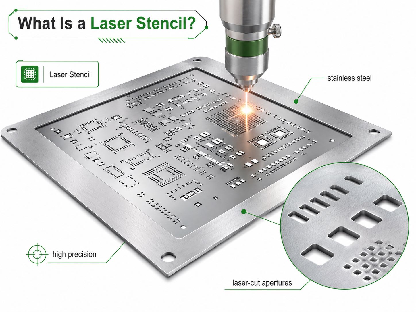
What Is a Laser Stencil?

A laser stencil is a solder paste stencil made by laser cutting. The apertures are cut directly from the design data, usually from Gerber or CAD files.

Laser stencils are widely used because they offer:

  • High aperture accuracy
  • Clean opening geometry
  • Good repeatability
  • Fast production
  • Fine-pitch support
  • Compatibility with electro-polishing
  • Stable SMT printing performance

At EBest Circuit, most SMT stencils are laser cut. Etched stencils are also available when the project requirements are suitable.

Laser cut stencils are especially useful for:

  • BGA packages
  • Fine-pitch ICs
  • QFN and DFN packages
  • 0201 and 0402 components
  • High-density PCB layouts
  • Medical electronics
  • Communication modules
  • Automotive PCBA
  • Industrial control boards

For better paste release, laser cut stencils can be electro-polished. Smooth aperture walls help solder paste release more easily, reduce cleaning frequency, and improve SMT printing efficiency.

solder paste stencil

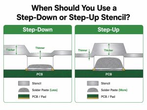
When Should You Use a Step-Down or Step-Up Stencil?

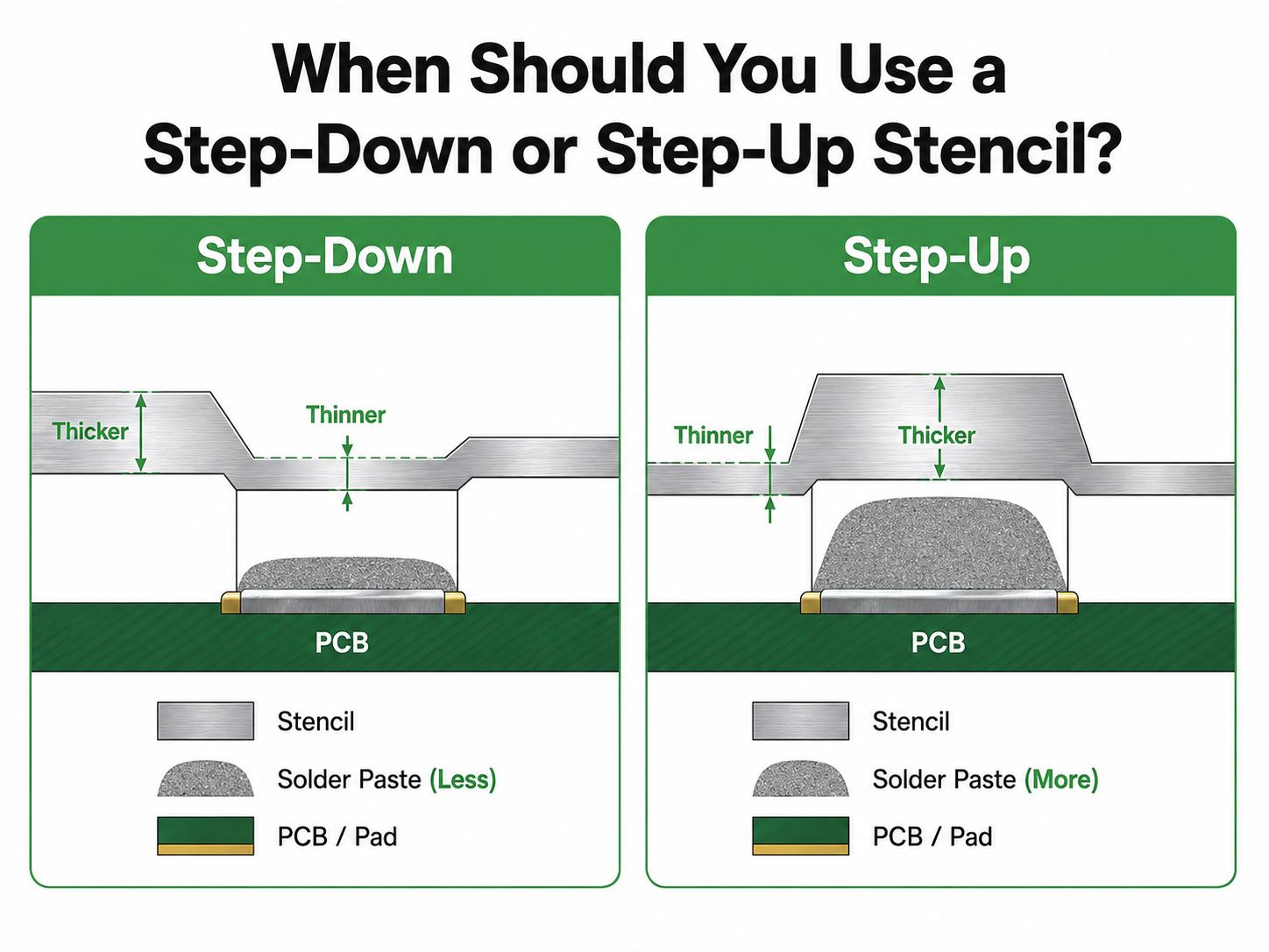
A step-down stencil has selected areas that are thinner than the main stencil. A step-up stencil has selected areas that are thicker than the main stencil.

These designs are used when different components on the same PCB need different solder paste volumes.

Stencil DesignFunctionTypical Use
Step-downLess paste locallyFine-pitch IC
Step-upMore paste locallyConnector pad
Mixed stepDifferent paste levelsComplex PCB

Use a step-down stencil when:

  • Fine-pitch ICs are bridging
  • Small components need less paste
  • QFN areas need tighter paste control
  • BGA areas require stable deposits
  • Dense layouts have limited spacing

Use a step-up stencil when:

  • Connectors need stronger joints
  • Large terminals need more solder
  • Shielding parts need higher paste volume
  • Special pads require extra solder height

Step stencil design should be reviewed carefully. The step edge should not be too close to active apertures. If the step area is too near component pads, the squeegee may not print evenly.

For many boards, aperture modification is enough. Step-up or step-down technology is more useful when aperture changes alone cannot balance solder volume.

solder paste stencil

Common Solder Paste Stencil Problems and Solutions

Many SMT defects begin at the solder paste printing stage. A good stencil can reduce these issues, but process control is also important.

DefectLikely CauseSolution
BridgingToo much pasteReduce aperture
Insufficient solderPoor releaseClean or adjust stencil
Missing pasteBlocked apertureClean stencil
Offset pasteBad alignmentCheck fiducials
TombstoningUneven pasteBalance apertures
Solder ballsExcess pasteUse better aperture
QFN floatingLarge center pasteUse window-pane
BGA openLow paste volumeCheck aperture
VoidingPoor pad designSegment aperture
Frequent cleaningRough wallsUse polishing

A stencil problem is more likely when the defect appears repeatedly in the same area. A process problem is more likely when the defect appears randomly across the board.

For example:

  • Same IC pins bridge every time: check aperture width.
  • Same QFN floats after reflow: check thermal pad opening.
  • Random missing paste: check stencil cleaning and paste condition.
  • Paste offset on many pads: check alignment and PCB support.

SPI inspection is useful here. It can check solder paste area, volume, height, thickness, short risk, and offset before components are placed. This makes stencil and printing problems easier to catch early.

How Long Can a Solder Paste Stencil Be Used?

A solder paste stencil does not last forever. In regular SMT production, its service life is usually around 50,000 prints. However, this number is not the only standard. The actual usable life depends on stencil tension, printing frequency, aperture wear, cleaning condition, storage time, and whether the stencil can still provide stable solder paste release.

In production, stencil life is usually checked by:

  • Printing count
  • Frame tension
  • Aperture wear
  • Paste release quality
  • Cleaning result
  • Storage time
  • Production history
Check ItemPractical StandardWhy It Matters
Printing countAround 50,000 printsTracks stencil usage
Stencil tensionScrap if ≤25NKeeps printing stable
Aperture wearCheck visuallyAffects paste shape
Paste releaseCheck print resultAffects solder volume
Cleaning resultNo blocked aperturesPrevents missing paste
Storage timeReview after long idle timeAvoids old tooling risk
Repeat order gapReview if no order for 3 yearsConfirms stencil reliability

For framed stencils, tension should be checked before and after use. The measurement should not be taken at only one point. It is better to check the four corners and the center area, because uneven tension can cause local solder paste printing defects.

If the stencil tension becomes weak, the printing count is over the control limit, the apertures are worn, or the stencil has been stored for too long, printing stability may decrease. For repeat PCB orders after a long gap, the old stencil should be inspected before reuse. If it no longer meets the production requirement, making a new stencil is safer than risking unstable SMT printing.

What Files Are Needed to Make a PCB Stencil?

To make a solder paste stencil, the paste layer is the key file. However, for better assembly results, the supplier should review more than one file.

FilePurpose
GerberPCB data
Paste layerAperture source
BOMPackage check
Pick-and-PlacePosition check
Assembly drawingPolarity and side
Panel drawingProduction layout
Special notesProcess needs

The required data may come from different file formats, such as Gerber, PCB, CAD, Protel, or other electrical design files.

Direct data input from customer files helps reduce manual conversion errors. It also makes stencil production faster and more accurate.

Before ordering a stencil, confirm:

  • Top side or bottom side
  • Single stencil or two stencils
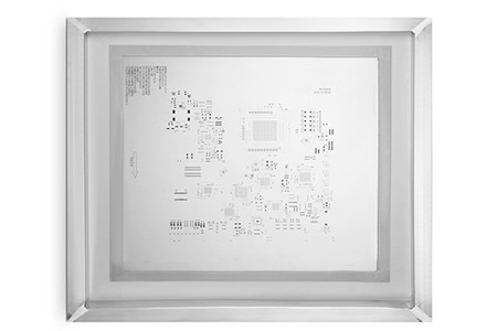
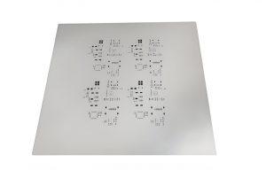
  • Framed or frameless type
  • Stencil thickness
  • Fiducial marks
  • Step-up or step-down areas
  • BGA or QFN requirements
  • Long board or LED strip requirement
  • Shipping and packaging needs

For PCB assembly projects, it is better to send Gerber, BOM, and Pick-and-Place files together. This helps the engineering team check whether the stencil design matches the actual component layout.

How Does EBest Circuit Support SMT Stencil Projects?

EBest Circuit provides SMT stencil support for prototype PCB assembly, low volume PCB Assembly, and production projects. Most of our SMT stencils are laser cut. Etched stencils are also available for suitable applications.

Our stencil service covers both standard and special requirements.

CapabilitySupport
Lasercut stencilAvailable
Etched stencilOptional
Framed stencilAvailable
Frameless stencilAvailable
Stainless steel stencilStandard
PE stencilOptional
Electro-polishingAvailable
Fiducial marksCustom position
Step-up/down stencilAvailable
BGA ball mounting stencilAvailable
LED strip PCB stencilAvailable

Our stencil advantages include:

  • Fast stencil preparation after file confirmation
  • Direct use of customer design files
  • Framed and unframed stencil options
  • Stainless steel material for stable printing
  • Laser cut apertures for high accuracy
  • Electro-polished apertures for better paste release
  • Smooth opening walls to reduce cleaning frequency
  • Tapered aperture walls to support paste transfer
  • Fiducial marks based on project needs
  • Step-up and step-down options for mixed components
  • Careful packaging to protect the stencil during transport

EBest Circuit also supports PCB fabrication and SMT assembly, so stencil review can be linked with the full PCBA process. This is important because stencil quality should not be judged only by the metal sheet. It should be judged by the solder paste printing result and the final assembly quality.

For projects with BGA, QFN, fine-pitch IC, LED metal core PCB, connectors, or long strip boards, our team can review stencil thickness and aperture design before production. This helps reduce common SMT risks and improves process stability.

How to Choose a PCB Stencil Manufacturer for SMT Assembly

Choosing a PCB stencil manufacturer is not only about price. A low-cost stencil may still cause expensive rework if the aperture design, material, or thickness is not suitable.

A reliable stencil supplier should understand both stencil fabrication and SMT assembly.

Evaluation PointWhat to Check
File reviewGerber and paste layer
Thickness adviceBased on components
Aperture designFine-pitch support
Special processStep-up/down
Surface qualitySmooth release
DeliveryProduction schedule
PackagingTransport safety
Assembly feedbackSPI/AOI/X-ray link

A good supplier should be able to answer:

  • Why is this thickness selected?
  • Should the BGA aperture be reduced?
  • Does the QFN pad need window-pane design?
  • Is step-down technology necessary?
  • Is the board suitable for framed or frameless stencil?
  • Will long strip PCB need special support?
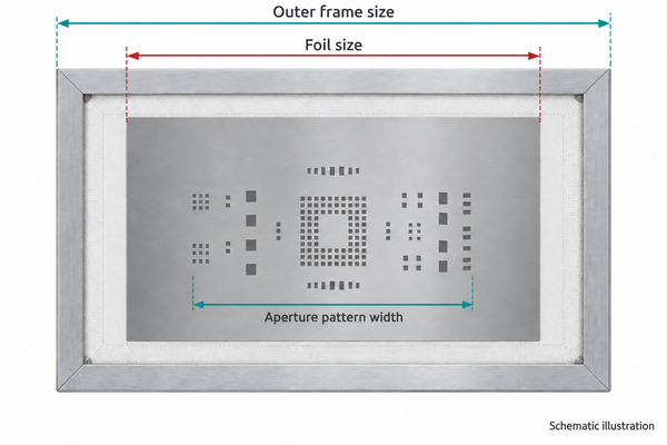
  • Can the stencil fit the SMT printer frame?

If a supplier only cuts the paste layer without checking the assembly situation, the stencil may still be usable, but it may not be optimized.

For complex PCBA projects, it is better to work with a partner who can review PCB, stencil, solder paste printing, placement, reflow, and inspection together.

Solder Paste Stencil Design Checklist

Before stencil production, use this checklist to reduce avoidable issues.

File checklist

  • Gerber files are complete
  • Paste layer is included
  • BOM is available
  • Pick-and-Place file is ready
  • Assembly drawing is clear
  • Panel drawing is confirmed

Design checklist

  • Stencil thickness is selected
  • Aperture reductions are reviewed
  • BGA areas are checked
  • QFN exposed pads are segmented
  • Fine-pitch ICs are reviewed
  • LED thermal pads are checked
  • Connector pads are reviewed

Production checklist

  • Framed or frameless type is confirmed
  • Fiducial marks are included
  • Step areas are defined
  • Printer frame size is suitable
  • PCB support method is clear
  • SPI inspection is planned
  • Packaging method is confirmed

Risk checklist

  • Mixed components on one side
  • Small 0201 or 0402 parts
  • Fine-pitch ICs
  • Large exposed pads
  • Long strip LED boards
  • Heavy connectors
  • Double-sided SMT
  • Old stencil reuse

This checklist is useful for both prototype and batch production. It helps buyers and engineers discuss stencil details before defects appear on the SMT line.

FAQs About Solder Paste Stencil

How long can a solder paste stencil be used?
A solder paste stencil can usually be used for about 50,000 prints in regular SMT production. Its actual life depends on stencil tension, print count, aperture wear, cleaning quality, and storage condition.

When should an SMT stencil be scrapped?
An SMT stencil should be scrapped if the measured tension is ≤25N, if the print count exceeds 50,000 cycles, or if it has not been used for a customer order for around 3 years. In these cases, the stencil may no longer provide stable solder paste printing.

How should stencil tension be checked?
Stencil tension should be checked before and after use. The measurement should cover the four corners and the center area, not just one point, because uneven tension can cause local printing defects.

What solder paste printing problems can SPI detect?
SPI can detect solder paste volume, area, thickness, height, depth, offset, and short-circuit risk. It helps catch printing issues such as missing paste, offset paste, solder bridging, insufficient solder, and paste peaks before component placement.

What are common solder paste stencil thicknesses?
Common stencil thicknesses include 0.06mm, 0.08mm, 0.10mm, 0.12mm, 0.15mm, and 0.20mm. For many SMT PCB assembly projects, 0.10mm, 0.12mm, and 0.15mm are frequently used, while special designs may require thinner, thicker, or step-up/down stencils.

On the whole, a solder paste stencil is a key process tool in SMT PCB assembly. It controls solder paste volume, printing accuracy, aperture release, and the first condition for good solder joints.

A suitable stencil should match the PCB design, component package, paste type, production volume, and inspection requirements. For simple boards, a standard laser stencil may be enough. For fine-pitch ICs, BGAs, QFNs, connectors, LED metal core PCB, or mixed component layouts, stencil thickness and aperture design should be reviewed carefully.

EBest Circuit provides solder paste stencil support together with PCB fabrication and PCB assembly services. We support laser cut stencils, etched stencils, framed and frameless stencils, electro-polished apertures, fiducial marks, step-up/down technology, BGA ball mounting stencils, and stencil solutions for long strip LED metal core PCB.

If your project requires a solder paste stencil or complete SMT PCB assembly, you can send your Gerber files, BOM, Pick-and-Place file, and assembly requirements to sales@bestpcbs.com. Our engineering team can help review the stencil design before production and support your project from prototype to batch assembly.

You may also like

Your Trusted SMT Stencil Manufacturer – Precision & Reliability
Tuesday, January 27th, 2026

When searching for a professional SMT stencil manufacturer, BestPCBS stands out as the top choice for electronic manufacturers worldwide. Our decades of expertise in producing high-precision stencils make us the most reliable SMT stencil manufacturer for all your surface mount technology needs, from prototyping to mass production.

Why BestPCBS Is Your Top Choice for an SMT Stencil Manufacturer?

At BestPCBS, we combine advanced manufacturing technology with strict quality control to deliver SMT stencils that meet the highest industry standards. We offer 24/7 customer support, customizable solutions, and competitive pricing—factors that make us the preferred SMT stencil manufacturer for SMEs and large enterprises alike. Our on-time delivery rate exceeds 98%, ensuring your production lines never face delays.

Our Core Advantages

  • Precision: ±5μm aperture tolerance for fine-pitch components (01005, BGA, QFP)
  • Speed: 24-hour expedited service for urgent SMT stencil orders
  • Cost: 15% lower production costs compared to industry averages
  • Support: Dedicated engineering team for DFM reviews and technical guidance
SMT Stencil Manufacturer

What Defines a High-Quality SMT Stencil Manufacturer?

A high-quality SMT stencil manufacturer must master both technical precision and customer-centric service. At BestPCBS, we adhere to ISO 9001:2015 quality management standards, conducting 3 rounds of inspection before shipping any stencil. This commitment to quality ensures our stencils reduce solder defects by up to 70% for our clients.

4 Core Processes We Use for Custom SMT Stencil Manufacturing

Our custom SMT stencil manufacturing process is tailored to your specific PCB design requirements. We use four proven processes to cover all application scenarios, ensuring optimal solder paste transfer and long stencil lifespan:

ProcessPrecisionIdeal For
Laser Cutting≤5μmHigh-volume production
Electroforming≤3μmUltra-fine pitch components
Chemical Etching≤10μmLow-cost prototypes
Hybrid Process≤4μmMixed-technology PCBs

How We Ensure High-Precision SMT Stencil Production at BestPCBS

High-precision SMT stencil production starts with advanced equipment and skilled engineers. We use CNC laser cutters and 3D measuring systems to verify every aperture, ensuring positional accuracy within ±2μm. This level of precision directly improves PCB assembly yield by 10-15% for our customers.

Industrial-Grade Materials for Durable SMT Stencils

We only use industrial-grade SUS301 and SUS304 stainless steel for our SMT stencils, providing 400,000+ printing cycles per stencil—20% more than standard materials. For flexible PCB applications, we offer Kapton stencils with reinforced edges for added durability.

SMT Stencil Quality Inspection Standards at BestPCBS

Our SMT stencil quality inspection process includes three critical steps: dimensional verification, tension testing (35-50N/cm²), and surface finish inspection. Every stencil is tested on a dummy PCB to confirm solder paste transfer efficiency before delivery, eliminating post-shipping issues.

How to Reduce SMT Stencil Costs Without Compromising Quality

SMT stencil cost optimization is a key focus at BestPCBS. We offer bulk pricing discounts, design optimization suggestions to reduce material waste, and reusable stencil frames to lower long-term costs. Our engineering team reviews your PCB design for free to identify cost-saving opportunities without sacrificing performance.

Short Lead Time for SMT Stencils: Our Expedited Service

We understand the urgency of production deadlines, which is why our SMT stencil lead time starts at 24 hours for expedited orders and 3-5 business days for standard orders. We offer free express shipping on all expedited orders, ensuring your stencils arrive on time, every time.

FAQ: Common SMT Stencil Issues & BestPCBS’s Solutions

Q1: Why is my SMT stencil causing solder bridges?

A: Solder bridges are often caused by oversized apertures or poor surface finish. We calibrate aperture sizes based on your solder paste type and offer electro-polished stencils to reduce solder adhesion, eliminating bridge defects.

Q2: How can I extend the life of my SMT stencil?

A: Regular cleaning with ultrasonic cleaners and proper storage (23±3°C, 40-60% humidity) extends stencil life. We provide a free maintenance guide with every order to help you maximize stencil usage.

Q3: Can you modify an existing SMT stencil?

A: Yes, our engineering team can modify apertures or repair minor damage to existing stencils, saving you the cost of a full replacement. Modifications are completed within 12 hours for urgent requests.

Q4: Do you offer DFM reviews for SMT stencil designs?

A: Yes, we provide free SMT stencil design for manufacturability reviews to identify potential printing issues before production, reducing rework and delays.

Q5: What after-sales support do you provide?

A: We offer a 30-day warranty on all stencils and 24/7 technical support. Our team can assist with stencil installation, cleaning, and troubleshooting via video call or email.

SMT Stencil Design for Manufacturability (DFM) Guidelines

Our SMT stencil design for manufacturability guidelines help optimize your PCB design for efficient stencil production. We recommend aperture sizes 1.5x the stencil thickness, rounded aperture corners to reduce stress, and spacing guidelines for fine-pitch components to avoid printing defects.

After-Sales Support for Our SMT Stencil Customers

Our SMT stencil after-sales support doesn’t end with delivery. We offer free technical training for your production team, stencil repair services, and replacement parts for frames and gaskets. Our customer support team responds to all inquiries within 1 business hour.

Case Studies: Successful SMT Stencil Projects by BestPCBS

We’ve supplied SMT stencils to leading electronics manufacturers in automotive, medical, and consumer electronics industries. One medical device client saw a 25% reduction in solder defects after switching to our high-precision stencils, while an automotive client reduced production downtime by 30% with our short lead time service.

SMT stencil manufacturer

sales@bestpcbs.com

If you’re currently using an SMT stencil manufacturer that doesn’t meet your quality, speed, or cost requirements, it’s time to switch to BestPCBS. We offer a free sample stencil (up to 100x100mm) for new customers to test our quality firsthand. Contact us at sales@bestpcbs.com to place your order or request a quote—our team is ready to help you optimize your SMT stencil supply chain today.

You may also like

How to Make a Stencil: Expert Guide for Precision & Durability
Monday, January 26th, 2026

How to Make a Stencil: 2 Methods for Beginners & Pros

Learning how to make a stencil is a valuable skill for DIY projects, crafts, and even professional applications like PCB assembly. Mastering how to make a stencil correctly ensures clean, consistent results whether you’re using basic hand tools or advanced cutting machines. This guide breaks down two reliable methods—handmade for beginners and machine-assisted for precision—to suit different skill levels and project needs.

What Materials Do You Need to Make a Stencil?

How to Make a Stencil: Expert Guide for Precision & Durability

Essential Supplies for All Methods

  • Stencil substrate: Mylar, PVC sheets (0.3-0.5mm thickness), or plastic dividers for reusability; cardstock for one-time use.
  • Cutting tools: X-Acto knife (sharp #11 blade) for hand cutting; vinyl cutter or laser cutter for machine methods.
  • Auxiliary tools: Cutting mat, packing tape, spray adhesive, sandpaper, and tweezers for detail work.
  • Design tools: Printer, pencil, black marker, and graphic software (CorelDRAW, Adobe Illustrator) for digital designs.

How to Choose the Right Stencil Material?

MaterialBest ForProsCons
MylarReusable stencilsDurable, waterproof, heat-resistantSlightly higher cost than PVC
PVC SheetsDIY & small-batch useLow-cost, easy to cut, flexibleNot ideal for high-heat applications
CardstockOne-time projectsBudget-friendly, instant availabilityProne to warping when wet

Step-by-Step Guide to DIY Handmade Stencils

For Beginners (No Special Tools Needed)

  1. Prepare your design: Print or draw a bold, simple design (avoid thin lines). For text, use thick fonts to prevent breakage.
  2. Secure the design: Tape the printed design to the back of your transparent substrate to align cuts accurately.
  3. Cut carefully: Hold the X-Acto knife at 45°, cut along the design’s outer edges first, then inner details. Use a cutting mat to protect surfaces.
  4. Remove excess material: Use tweezers to pull out hollow sections (e.g., centers of letters like “O” or “A”).
  5. Trim edges: Sand rough edges lightly for clean lines and better paint adhesion.

How to Make a Stencil with a Cutting Machine?

For Precision & Complex Designs

For intricate patterns or mass production, use a vinyl cutter or laser cutter. Import your design into the machine’s software, adjust size and cut settings (speed: 3-5mm/s, pressure: 100-150g for vinyl), and load the substrate.

Laser cutters work best for Mylar or stainless steel (for professional SMT stencils). After cutting, peel the stencil from the backing and test for loose sections before use.

Design Tips for Durable & Precise Stencils

Avoid Common Design Mistakes

  • Add “bridges”: Connect small hollow areas (islands) to the stencil frame to prevent tearing. Bridges should be at least 1mm wide.
  • Keep it simple: Beginners stick to large shapes; save fine details for machine-cut stencils.
  • Size strategically: Make the stencil 1-2cm larger than the target design for easier handling.

How to Test & Touch Up Your Stencil?

Test the stencil on scrap material before final use. If edges bleed, apply thin tape to seal gaps. For minor tears, use clear tape on the stencil’s back to reinforce without blocking the design. Replace the stencil if tears are too large to repair.

Common Applications of Homemade Stencils

Homemade stencils work for wall decor, fabric painting, signage, and hobby PCB projects. For professional electronics assembly, however, precision SMT stencils are required to apply solder paste accurately to tiny components.

How to Make a Stencil: Expert Guide for Precision & Durability

FAQ: Troubleshooting Stencil Making Issues

  • Q: Why do my stencil edges have burrs? A: Use a sharper blade, cut slower, or switch to a thinner substrate. Sanding after cutting also helps.
  • Q: How to prevent paint bleeding under the stencil? A: Apply light, thin coats of paint and use spray adhesive to secure the stencil tightly.
  • Q: My stencil tears easily—what’s wrong? A: Lines or bridges are too thin. Redesign with wider bridges (≥1mm) or use a more durable material like Mylar.
  • Q: Can I reuse a paper stencil? A: Paper stencils are for one-time use; switch to Mylar or PVC for reusable options.
  • Q: How to fix a misaligned design? A: Secure the design to the substrate with multiple tape points before cutting to prevent shifting.
  • Q: Why won’t my cutting machine cut through the substrate? A: Adjust the blade depth or pressure; ensure the material is compatible with the machine.

How to Extend the Service Life of Your Stencil?

Clean the stencil immediately after use with mild soap and water (avoid harsh chemicals). Store flat in a dry place to prevent warping. For plastic stencils, apply a thin layer of clear nail polish to edges to reinforce durability.

Differences Between DIY Stencils & Professional Stencils

DIY stencils are cost-effective for small projects but lack the precision of professional options. Professional stencils (e.g., laser-cut stainless steel) offer tight tolerances, durability for high-volume use, and are essential for applications like PCB assembly where accuracy is critical.

Where to Get High-Quality Custom Stencils?

For projects requiring professional-grade precision—such as SMT stencils for PCB assembly—we offer high-quality custom stencils tailored to your design specifications. Our stencils are laser-cut for accuracy, made with durable materials, and suitable for both prototype and small-batch production. Need a custom stencil? Place your order by emailing us at sales@bestpcbs.com.

You may also like

What Is an SMT Stencil? A Complete Guide for Engineers
Monday, January 26th, 2026

What is an SMT Stencil?

An SMT Stencil (Surface Mount Technology Stencil) is a precision tool used in PCB assembly to deposit accurate amounts of solder paste onto specific pads of a printed circuit board. This tool acts as a template, ensuring solder paste is applied only where needed for component mounting. The SMT Stencil is a core component of the SMT printing process, directly impacting soldering quality and production efficiency.

Key Functions of SMT Stencils in PCB Assembly

Why Is an SMT Stencil Indispensable?

  • Controls solder paste volume: Delivers exact quantities to prevent insufficient soldering or bridging.
  • Ensures positional accuracy: Aligns with PCB pads to avoid offset paste application.
  • Boosts production speed: Enables uniform, rapid paste printing for mass assembly.
  • Supports diverse components: Adapts to fine-pitch parts (QFP, BGA) and small chips (0201).

Common Types of SMT Stencils

Which Type Fits Your Project?

Stencil TypeKey FeaturesIdeal Applications
Laser Stencil±4μm accuracy, trapezoidal aperturesFine-pitch components, high-precision PCBs
Electropolished (E.P.) StencilSmooth hole walls, reduced wiping frequencyQFP, BGA, CSP with ultra-fine spacing
Step StencilVariable thickness on one stencilPCBs with mixed component solder demands
Electroformed (E.F.) StencilCustom thickness, superior smoothnessuBGA, 0201 chips, ultra-dense PCBs

SMT Stencil Manufacturing Processes: Pros & Cons

Three Main Production Methods

  • Laser Cutting: High precision (minimal human error), trapezoidal apertures for better paste release. Cons: Slower production for complex designs.
  • Chemical Etching: Fast one-step molding, low cost. Cons: Hourglass-shaped apertures, poor accuracy for fine-pitch parts.
  • Electroforming: Smooth hole walls, ideal for ultra-fine spacing. Cons: Long lead time, high cost, environmental impact.

How to Choose the Right SMT Stencil Thickness?

SMT stencil thickness directly determines solder paste volume. For most PCBs, 0.12-0.15mm is standard. Choose 0.08-0.10mm for fine-pitch components (pitch ≤0.3mm) and 0.18-0.20mm for large pads or adhesive printing. Align thickness with component type—BGA typically uses 0.15-0.18mm, while 0201 chips need 0.08-0.10mm.

SMT stencil, SMT stencil thickness, SMT stencil aperture design, laser SMT stencil, electropolished SMT stencil, SMT stencil cleaning, SMT stencil paste release, SMT stencil manufacturing, step SMT stencil, SMT stencil quality

Critical Guidelines for SMT Stencil Aperture Design

Aperture Ratio & Aspect Ratio Rules

To ensure good paste release, maintain an aspect ratio >1.5 (aperture width/stencil thickness) and area ratio >0.66 (aperture area/hole wall area). For apertures with length <5x width, use area ratio; otherwise, use aspect ratio.

Component-Specific Aperture Tips

  • QFP (0.3-0.635mm pitch): Aperture width = 85-90% of pad width, rounded corners to avoid stress.
  • BGA: Circular apertures (75-90% of pad diameter) or square apertures for uBGA.
  • 0603+ chips: Concave apertures to prevent solder balls and tombstoning.

Materials Needed for SMT Stencil Production

Provide manufacturers with these core materials to ensure accuracy:

  • PCB file (Gerber, PCB, DXF, or PDF) with solder paste layer and fiducial marks.
  • CAD data (Protel, PowerPCB, AutoCAD) including pad layout and PCB outline.
  • PCB sample (if no digital files) to verify pad positions and print surface.
  • Special requirements: Step thickness, electropolishing, or nickel plating.
SMT stencil, SMT stencil thickness, SMT stencil aperture design, laser SMT stencil, electropolished SMT stencil, SMT stencil cleaning, SMT stencil paste release, SMT stencil manufacturing, step SMT stencil, SMT stencil quality

Tips to Improve SMT Stencil Paste Release

  • Optimize aperture geometry: Trapezoidal apertures (upper 1-5mil larger than lower) for smooth release.
  • Electropolish apertures: Reduces friction between solder paste and hole walls.
  • Nickel plating: Enhances surface smoothness, ideal for fine-pitch applications.
  • Control stencil tension: Proper tension (30-35N/cm) prevents deformation during printing.

Maintenance & Cleaning of SMT Stencils

Daily Maintenance Routine

  • Wipe stencil after 50-100 prints: Use alcohol-based cleaner to remove residual paste.
  • Ultrasonic cleaning weekly: Deep clean apertures to avoid paste buildup.
  • Inspect for damage: Check for bent frames, torn mesh, or deformed apertures before use.
  • Store in dry environment: Prevent rust and contamination of stainless steel surfaces.

FAQ: Common SMT Stencil Issues & Solutions

  • Q: Why is solder bridging occurring? A: Reduce aperture width by 5-10%, check stencil alignment, or lower printing pressure.
  • Q: Insufficient solder paste on pads? A: Increase aperture size (within ratio limits), thicken stencil, or optimize paste viscosity.
  • Q: Paste sticking to stencil apertures? A: Electropolish the stencil, increase wipe frequency, or use a release agent.
  • Q: Uneven paste deposition? A: Check stencil flatness, adjust printing speed, or replace worn squeegees.
  • Q: Solder balls forming around components? A: Use concave apertures for chips, reduce paste volume, or improve reflow profile.
  • Q: Stencil misalignment with PCB? A: Calibrate fiducial marks, check PCB warpage, or adjust stencil frame tension.

How Does SMT Stencil Quality Affect Soldering Results?

Poor SMT stencil quality causes 40% of SMT soldering defects. Inaccurate apertures lead to bridging or insufficient solder; rough hole walls cause paste residue and inconsistent deposition. High-quality SMT Stencils (laser-cut, electropolished) reduce defect rates by up to 70% and improve production yield.
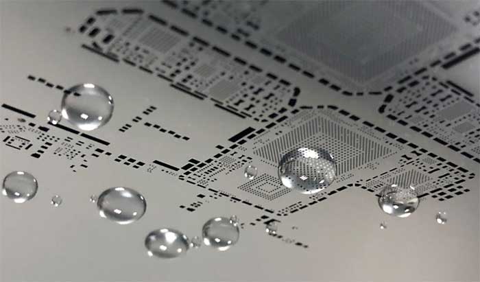

Latest Trends in SMT Stencil Technology

As PCBs become denser, SMT stencil tech evolves: Nickel-plated stencils gain popularity for better paste release; 3D-printed stencils offer rapid prototyping; smart stencils with embedded sensors monitor tension and alignment in real time. These innovations adapt to ultra-fine-pitch components and high-volume production demands.

We provide high-precision SMT Stencil products tailored to your PCB assembly needs, including laser, electropolished, and step stencils. All our stencils comply with IPC-7525 standards and ensure optimal soldering performance. For orders or inquiries, please contact us at sales@bestpcbs.com.

You may also like