PCB manufacturing PCB manufacturing
Home > Blog

Metal Core PCB Manufacturers in Spain: Companies, Capabilities and Sourcing Options

September 2nd, 2026

Metal Core PCB manufacturers in Spain include CIRLAN, Fast PCB, Maxwell Atlantic and CIPSA Circuits. The useful differences are practical: which IMS structures they describe, what quality controls they disclose, whether they publish a lead time, and whether they supply only bare boards or can cover a wider manufacturing scope.

If you are sourcing an aluminium or copper-base PCB, start with the structure and delivery requirement. A single-sided lighting board, a double-sided PTH IMS design and a fully assembled thermal board do not belong in the same RFQ. The comparison below shows what each supplier publicly offers and which details still need a written quotation.

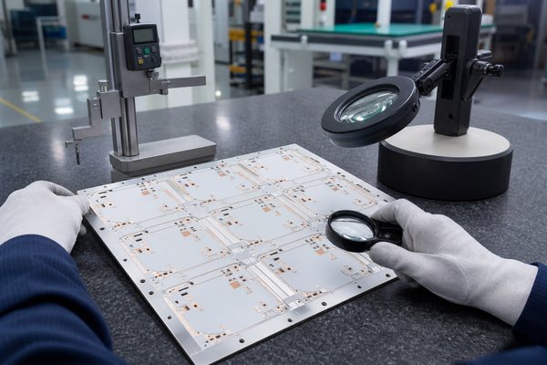
Metal Core PCB manufacturers in Spain, aluminium and copper IMS panels in a quality inspection lab

Who Are the Main Metal Core PCB Manufacturers in Spain?

CIRLAN, Fast PCB, Maxwell Atlantic and CIPSA Circuits all identify finished PCB manufacturing operations in Spain and publish an IMS or metal-core offer. Their process scope and delivery visibility are not the same.

Company Process capability Lead-time information Service scope
CIRLAN
Urnieta, Gipuzkoa
Single-sided aluminium and copper IMS; published standard and special dimensional ranges No standard IMS turnaround published; factory route and committed date belong in the quote Engineering, optimisation, panelisation and bare PCB manufacturing; some technologies may use Shenzhen partners
Fast PCB
Irún, Gipuzkoa
Single-sided aluminium IMS; 0.8–3.2 mm base, 35–105 µm copper and 100 m²/day stated capacity Short series: 5 working days
Large series: 10 working days
Bare PCB prototypes and series; routing, V-scoring, chemical tin and optional production certificate
Maxwell Atlantic
Santiago de Compostela
Aluminium or copper IMS within an in-house single-, double- and multilayer PCB process No standard IMS turnaround published; ask for prototype and repeat-order dates separately Bare PCB manufacturing for prototypes and small, medium or large series; in-house inspection and traceability
CIPSA Circuits
Rubí, Barcelona
Aluminium IMS, including single-sided, isolated-hole, double-sided and PTH structures General PCB prototype service: 24 hours to 5 days; confirm that the quoted IMS build qualifies Bare PCB prototypes and series with process testing and lot traceability

Match the shortlist to the actual build before requesting prices. Fast PCB publishes defined timing for single-sided aluminium IMS; CIRLAN provides aluminium and copper single-sided process limits; CIPSA documents double-sided and PTH aluminium structures; and Maxwell Atlantic offers broad in-house PCB inspection and traceability. Send the same material, quantity, test, dispatch-date and delivery-price requirements to the relevant suppliers so their quotations cover the same work.

CIRLAN

CIRLAN publishes one of the clearest Spanish process windows for single-sided aluminium and copper IMS. Its aluminium range lists 1.0, 1.5, 2.0 and 3.0 mm board thicknesses. Standard copper is 35 or 70 µm; 105 µm is listed as special production. The same table gives track and spacing, drill, routing, scoring, panel-size and finish limits.

That detail helps a buyer see whether a conventional IMS design falls inside the standard column before requesting a quote. It does not publish a standard turnaround or price. Ask CIRLAN to identify the dielectric grade, thermal data, metal alloy, inspection package and dispatch date for the released files.

CIRLAN separates local services from outsourced technologies. Its local scope includes engineering, optimisation, panelisation, aluminium IMS and copper IMS. The company also describes cooperation with PCB factories in Shenzhen for other technologies. If Spain production is a purchasing condition, the quotation should name the physical plant for the exact part.

Fast PCB

Fast PCB is the easiest supplier in this group to assess when the project is a conventional single-sided aluminium board and delivery speed matters. Its IMS page states 5 working days for short series, 10 working days for large series and 100 m²/day of production capacity.

The published process range covers aluminium bases from 0.8 to 3.2 mm, copper from 35 to 105 µm, a maximum delivery format of 544 × 390 mm, chemical tin, CNC routing and V-scoring. That is enough to reject obvious mismatches before engineering spends time on an RFQ.

Fast PCB also describes a metallographic laboratory that performs ageing tests, thermal shock, digital microsection measurement and solderability checks. A production certificate can be supplied with the order on request. Put the required report, sampling level and acceptance criteria into the purchase specification; do not assume every report is included in the unit price.

Its public IMS offer is specifically single-sided aluminium. Copper-base, plated-through-hole, double-sided IMS and alternative finishes need an explicit technical answer and separate schedule.

Maxwell Atlantic

Maxwell Atlantic is relevant when a buyer wants broad in-house PCB process control as well as an aluminium or copper IMS option. The Santiago de Compostela company states that its PCB manufacturing is carried out without third-party subcontracting and can cover prototypes plus small, medium and large series.

Its listed equipment and processes include CNC drilling and milling, lamination, single-, double- and multilayer etching, electroplating, desmear, AOI, solder-mask processing, laser marking and flying-probe electrical test. The quality system follows UNE-EN-ISO 9001, and the company describes full traceability for raw materials and test results.

This is useful quality evidence, but the public pages do not provide an IMS-specific lead-time table or detailed metal-core process window. The quotation should therefore state the exact IMS structure, dielectric, thermal and isolation values, PTH method, inspection reports, quantity break and committed dispatch date. Ask for the IMS limits, not a general PCB capability list.

CIPSA Circuits

CIPSA Circuits publishes the widest aluminium IMS structure range among the four companies compared here. Its capability material covers single-sided boards, isolated holes, openings in the aluminium, double-sided PTH with an aluminium base and double-sided constructions with an aluminium core. Several structures list 35 or 70 µm copper and 0.15 mm line and spacing.

CIPSA states on its quality page that it performs rigorous controls throughout manufacturing and retains traceability for raw materials and test results. Its general prototype service runs from 24 hours to 5 days and uses the same production lines and finishes as series manufacture. Because that timing page covers PCB prototypes broadly, ask CIPSA to confirm whether the actual IMS material and construction qualify for the requested expedite window.

CIPSA is a strong technical candidate for aluminium IMS that goes beyond a basic single-sided board. Copper-core IMS, the current revision of the capability data, inspection deliverables, setup charges and freight to the final destination still need to appear in the quotation.

How Do These Metal Core PCB Manufacturers Compare?

Do not compare four unit prices until every quote covers the same material, tests, quantity, delivery point and service scope. A cheaper line item can become the expensive choice once tooling, certificates, freight or a second supplier for assembly is added.

Buyer concern What to compare What the quote should state
Quality IMS material identity, electrical test, isolation test, dimensional inspection, traceability and non-conformance handling Named material and factory, test method, sampling or 100% scope, reports supplied and acceptance criteria
Total price Unit price at prototype and repeat quantities, tooling, test reports, special material, packing, freight and import charges Separate line items, quotation validity, quantity breaks, Incoterm and currency
Lead time DFM response, material procurement, fabrication, test, packing and transit Clock start, working days, engineering-hold rule, dispatch date and arrival responsibility
Service scope Bare PCB only or PCB plus component sourcing, assembly, inspection, functional test and shipping Exact owner for each stage, included deliverables and warranty or failure-analysis route

Ask for two dates: the factory dispatch date and the expected delivery date at your site. A five-day fabrication promise is not a five-day delivered order if material approval, engineering questions or freight sit outside the quoted clock.

What Should You Check Before Choosing a Metal Core PCB Manufacturer?

Approve the complete thermal and commercial build, not just an “aluminium PCB” label. These checks prevent the most common gaps between an attractive quotation and the board that actually arrives.

  • Lock the thermal stack: name the IMS material, metal alloy, dielectric thickness, dielectric performance, finished copper and total board thickness. Ask whether the thermal value is typical or guaranteed.
  • Define electrical isolation: specify working voltage, test voltage, dwell time and acceptance limit. For PTH IMS, require the supplier to show how barrels and pads are isolated from the metal.
  • Control the mechanical interface: include outline, flatness, hole and slot tolerances, burr limits, countersinks, V-score and the heat-sink contact surface.
  • Check repeatability: ask which material and factory will be used for prototypes and series. Any material or site substitution should need written approval.
  • Match the inspection to the risk: define electrical test, isolation test, dimensional report, material certificate, first-article check and lot traceability. State which documents must ship with the boards.
  • Close the delivery assumptions: agree when the clock starts, what pauses it, which parts of the schedule are expedited and whether the promised date is dispatch or arrival.

For a pilot order, keep the supplier’s deviations list with the approved files. When the board moves into repeat production, compare the new material lot, factory, process and test plan against that record before release.
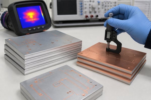
Metal Core PCB manufacturers in Spain, IMS stackup and quality checks before supplier approval

EBest Circuit – An Overseas Metal Core PCB Manufacturing Option for Spain

If the project does not require Spain-local fabrication, EBest Circuit can combine metal-core PCB fabrication, component sourcing, PCBA, inspection and testing under one order. That removes the handoff between a bare-board factory, a component buyer and an assembly house. One team reviews the Gerber or ODB++, stackup, BOM, placement data and test requirements before production.

For standard MCPCB prototypes below 1 m² using standard aluminium, 0.8–2.0 mm board thickness, H/H or 2 oz copper, lead-free HASL, white solder mask, black legend and 0.8 W/(m·K) material, EBest publishes these manufacturing references:

  • Single-layer MCPCB: 4 days standard, with a 24-hour fastest option;
  • Two-layer MCPCB: 14 days standard, with a 168-hour fastest option;
  • Four-layer MCPCB: 21 days standard; expedite timing is reviewed per design.

Copper-base, higher-conductivity, heavy-copper, special-finish, multilayer or custom-test builds need a project schedule. For full PCBA, the standard published reference is 10–12 business days from confirmed files and purchase order, subject to BOM availability and test scope.

The commercial advantage is a quote that can show the complete delivered scope: bare board, components, SMT or THT assembly, AOI, functional test, packing and freight to Spain. This makes the total cost easier to compare with a local bare-board quotation. EBest also provides a free DFM review, so material, isolation, panelisation and assembly risks can be raised before the order is released.

Use the same drawings, quantities and quality requirements when comparing EBest with Metal Core PCB manufacturers in Spain. Then compare the final delivered price and arrival date rather than bare-board price alone.

What Should You Include in a Metal Core PCB RFQ?

A complete RFQ reduces both price padding and schedule surprises. Send the same controlled package to every supplier:

  • Gerber or ODB++, drill files and revision-controlled fabrication drawing;
  • metal type and alloy, dielectric, finished copper and total thickness;
  • required thermal and electrical-isolation performance;
  • outline, slots, holes, countersinks, flatness, burr and V-score limits;
  • surface finish, solder mask, legend, panelisation and breakaway method;
  • electrical, isolation, dimensional and traceability deliverables;
  • prototype, pilot and repeat quantities, plus annual demand;
  • requested factory dispatch date, delivery address and Incoterm;
  • BOM, approved alternates, CPL, assembly drawing and test specification when PCBA is required.

Require the quotation to list deviations and exclusions beside the price. If the supplier proposes a different dielectric, omits a test or starts lead time only after a later approval, you should see that before comparing totals.
Metal Core PCB manufacturers in Spain, quality evidence and RFQ documents checked before ordering

FAQs About Metal Core PCB Manufacturers in Spain

Q1: Which Spanish supplier publishes a lead time for aluminium IMS?

A1: Fast PCB states 5 working days for short series and 10 working days for large series. CIPSA publishes a broader PCB prototype service of 24 hours to 5 days, but the requested IMS construction should be confirmed for that service.

Q2: Which companies publish copper IMS capability?

A2: CIRLAN and Maxwell Atlantic list copper as well as aluminium IMS. The quote should still identify the copper base, dielectric, factory and process limits for the part.

Q3: Which supplier publishes double-sided or PTH IMS structures?

A3: CIPSA publishes aluminium IMS options that include double-sided and PTH constructions. Ask for the current capability revision and the isolation method around plated features.

Q4: How should I compare metal core PCB prices?

A4: Compare the same material, quantity, tooling, tests, reports, packing, freight and delivery term. Separate bare-board and PCBA costs so missing work does not make one quote look artificially low.

Q5: What quality records should I request?

A5: Typical records include material identity, electrical-test results, isolation-test results, dimensional inspection, lot traceability and any agreed first-article report. Put required documents in the purchase order.

Q6: Does a short fabrication lead time include delivery to Spain?

A6: Usually not unless the quotation says so. Ask for the clock start, fabrication days, dispatch date, freight method and expected arrival date.

Q7: Can one supplier handle both metal-core PCB and assembly?

A7: Some overseas suppliers, including EBest Circuit, offer metal-core PCB fabrication, component sourcing, PCBA and testing together. The Spanish suppliers reviewed here mainly present bare PCB manufacturing services.

Q8: What files are needed for an accurate quotation?

A8: Send Gerber or ODB++, drills, stackup, fabrication drawing, thermal and isolation requirements, quantity and delivery target. Add BOM, CPL, assembly drawing and test instructions for PCBA.

Conclusion

The best supplier depends on the exact structure and delivery model. CIRLAN publishes detailed single-sided aluminium and copper IMS limits. Fast PCB provides the clearest stated series lead times for single-sided aluminium. Maxwell Atlantic offers broad in-house PCB processing and traceability. CIPSA publishes aluminium IMS structures that include double-sided and PTH options.

Compare quality evidence, total delivered cost, clock start, dispatch date and service scope before choosing. If you need a combined metal-core PCB and PCBA route for delivery to Spain, send Gerber or ODB++, stackup, quantities, BOM, CPL, assembly drawing, test requirements and target arrival date to sales@bestpcbs.com. EBest Circuit will provide a free DFM review and a project-specific quotation.
You may also like

How to Choose the Right Metal Core PCB Manufacturer in the USA?

August 28th, 2026

Choose a metal core PCB manufacturer in the USA by matching the released construction, evidence package, quantity profile, and assembly scope to the factory that will build the order. A suitable manufacturer must be able to control the specified metal base, dielectric, copper, hole isolation, mechanical features, surface finish, and assembly interface as one design.

Shortlist suppliers by project fit and order evidence. Confirm who will manufacture the board, which material and process route will be used, what records will accompany the order, and whether those controls remain stable from prototype through repeat production. This keeps the selection process focused on a manufacturable, verifiable board rather than a long list of unrelated capabilities.

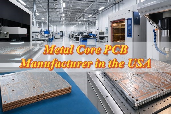
metal core PCB manufacturer in the USA, factory production floor with metal-core PCB panels and article title

What Should You Verify Before Shortlisting a Metal Core PCB Manufacturer Serving the USA?

Start with eight selection factors that determine whether a supplier can support the complete order. Remove candidates that cannot match the construction, evidence, quantity, or assembly scope before engineering time is spent on detailed quotations.

  • Relevant production history: Ask for evidence of work with the same MCPCB construction; standard single-sided aluminum experience does not qualify every metal-core build.
  • Metal-base range: Confirm the supported aluminum alloys, copper bases, thicknesses, and any special bonded or machined structures.
  • Thermal material control: Review dielectric grade, thickness, thermal performance, electrical isolation, and substitution policy together.
  • Custom construction capability: Match plated holes, multilayer bonding, pockets, routing, countersinks, and other drawing features to the proposed factory.
  • Order-level quality evidence: Define material, dimensional, electrical, isolation, and traceability records that will be released with the lot.
  • Assembly integration: If PCBA is required, check whether fabrication, soldering, heat-sink interfaces, inspection, and test ownership are coordinated.
  • Quantity fit: Confirm prototype support, intended production capacity, tooling, material availability, and repeat-order controls.
  • DFM response: A useful review identifies a specific drawing, material, isolation, machining, or assembly risk and returns a clear decision or question.

Which Metal Core PCB Construction Must the Manufacturer Prove?

Approve a supplier across the independent construction axes used by your design, because “metal core PCB” does not describe one manufacturing route. Separate the base material, circuit-layer structure, thermal-path architecture, electrical specialization, and mechanical integration before checking factory experience.

  • Base material axis: For aluminum, verify alloy, thickness, laminate, profiling, and panel control; for copper, add source control, weight, oxidation protection, machining, and handling.
  • Circuit-layer axis: A single-sided IMS route differs from a plated double-sided or multilayer route. Confirm hole isolation, bond sequence, registration, stackup limits, and internal-construction evidence as applicable.
  • Thermal-path axis: Distinguish a conventional dielectric-based path from a direct thermal path. Require a cross-section that shows both heat flow and electrical isolation.
  • Electrical-specialization axis: Power and LED IMS work emphasizes thermal and assembly control, while RF metal-backed work adds RF laminate handling, bond film, pockets, metal-carrier plating, dimensional datums, and finish compatibility.
  • Mechanical-integration axis: Separate a standard profiled base from a precision-machined carrier. Direct mounting to a heat sink, housing, or frame brings outline, holes, flatness, burr, pocket, and mounting surfaces into supplier qualification.
A supplier experienced with single-sided LED aluminum boards may still lack the plated, multilayer, direct-path, RF, or precision-machining controls required by another design. Ask the candidate to mark each axis as routine, conditional, or outside its current process window.

Which MCPCB Specifications Should You Confirm Before Choosing a Manufacturer?

Match the required stackup to a confirmed factory process window before approving a supplier. Best Technology publishes the following reference values in its single-layer MCPCB data and current product catalog. Use them for initial quotation screening. Only a build-specific review can confirm whether the required material, copper, geometry, thickness, layer count, and panel size can be produced together.

Capability item Best Technology reference range What to confirm for the order
Single-layer base material Aluminum, copper, or iron alloy Exact alloy, metal thickness, source, surface treatment, and whether the quotation uses the named material
Single-layer dielectric conductivity 0.8, 1.0, 1.5, 2.0, or 3.0 W/(m·K) Material manufacturer and grade, dielectric thickness, thermal resistance, dielectric strength, and substitution rule
Copper weight 0.5, 1.0, 2.0, or 3.0 oz; up to 10 oz is listed Finished copper, minimum line/space at that weight, etching tolerance, and inspection method
Single-layer board thickness 0.5–3.0 mm Finished-thickness tolerance, flatness, mounting interface, and panel handling
General MCPCB layer count 1–10 layers Released cross-section, plated-hole isolation, lamination sequence, registration, and factory history with that structure
General MCPCB board thickness 0.8–5.0 mm Whether the requested thickness is valid with the selected layer count, metal base, copper, machining, and panel size
Minimum line/space 4/4 mil, or 0.10/0.10 mm Applicable copper weight, conductor tolerance, annular features, and production inspection basis
Maximum board dimension 610 × 1625 mm Usable panel size, array orientation, tooling margin, dimensional tolerance, flatness, and shipment protection

Send the same drawing, cross-section, quantities, and evidence requirements to every shortlisted supplier. Require the quotation to identify which values are routine, which require engineering review, and which combinations are unavailable at the named factory.

How Do You Verify the Manufacturer’s Quality and Traceability?

Reliability is demonstrated when the supplier can connect its quality system to your material, revision, lot, tests, and changes. Verify the certificate’s legal entity, site, and scope, then require order-specific material, revision, lot, test, and change records.

  • Site and scope: Check the legal entity, factory address, certificate scope, and actual operations used for the proposed order.
  • Incoming materials: Confirm how the metal base, thermal laminate, copper, solder mask, and finish materials are identified and released.
  • Process traceability: Ask how work orders, material lots, inspection results, deviations, and final shipments remain linked.
  • Electrical controls: Define the net test and any isolation requirement with the test method, voltage or limit supplied by the approved specification.
  • Dimensional controls: Identify which holes, cutouts, thicknesses, flatness points, and datums receive recorded inspection.

  • Nonconformance handling: Require segregation, disposition authority, corrective action, and customer notification for deviations that affect fit or performance.
  • Change control: Specify which material, process, factory, tooling, or sub-supplier changes require approval before the next lot.

The useful output is a qualification record that states what was verified, what remains conditional, and which documents will be delivered with production. Avoid approving a supplier from a logo sheet or questionnaire that is not connected to the actual build route.
How Do Material and Thermal Controls Affect Supplier Qualification?

Select a manufacturer whose routine materials and process controls match the metal base already justified by the thermal, mechanical, electrical, and cost design. Material selection comes first; supplier qualification then verifies the factory controls needed for that base and construction.

For an aluminum PCB project

  • Material identity: Confirm the base alloy, thickness, approved thermal laminate, dielectric thickness, and substitution limits.
  • Profiling control: Review routing, punching where applicable, V-scoring, burr control, and panel-to-board flatness.
  • Repeatability: Ask how thermal material and base-metal lots are controlled across prototype and production orders.

For a copper core PCB project

  • Base handling: Confirm copper-base weight, sourcing, oxidation protection, machining, and in-process handling.
  • Construction complexity: Review bonding, direct-path features, plated isolation, pockets, and registration with a cross-section.
  • Commercial impact: Ask the supplier to separate material, machining, tooling, yield-sensitive features, and assembly costs in the quote.

Do not assume that a high-volume aluminum IMS line can automatically produce a copper pedestal, plated metal-core, or RF metal-backed design. Qualification follows the released structure, not the broad MCPCB category.

Which Thermal Material Records Should the Supplier Provide?

Thermal material must be compared as a system because conductivity alone does not define heat flow or insulation performance. Two laminates with the same nominal W/m-K value can use different dielectric thicknesses and therefore produce different thermal resistance and electrical margins.

  • Thermal conductivity: Record the published value, test basis, and grade instead of accepting an unlabeled number.
  • Dielectric thickness: Confirm the finished or nominal thickness used in the thermal and isolation assessment.
  • Thermal resistance: Compare the full dielectric path and relevant area instead of using the material conductivity headline by itself.
  • Dielectric strength: Tie the required electrical isolation to an approved test method and design margin.
  • Material identity: Lock the manufacturer, grade, and accepted equivalent route when consistency matters.
  • Substitution policy: Require approval before a supplier changes grade, thickness, or source, even if the nominal conductivity is unchanged.
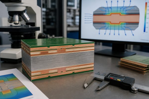
metal core PCB manufacturer in the USA, engineering review of copper dielectric and metal-base stackup

A strong candidate can return an approved stackup or material proposal that shows the copper, dielectric, and metal-base relationship. A weak candidate quotes “2 W/m-K” or “3 W/m-K” without naming the grade, dielectric thickness, isolation basis, or substitution boundary.

Can the Manufacturer Control Both Mechanical Fit and PCB Assembly?

Mechanical capability can disqualify an otherwise suitable MCPCB supplier when the board mounts directly to a heat sink, housing, or structural frame. Control the metal base as both a precision interface and a thermal layer.

  • Outline and datums: Define the dimensions that locate the board in the final assembly and the datum scheme used for inspection.
  • Slots and cutouts: State size, position, corner-radius, and burr requirements that affect clearance or fit.
  • Countersinks and countersunk holes: Specify side, angle, final diameter, depth, plating status, and relationship to the mounting hardware.
  • Routing and V-scoring: Confirm the separation method, residual thickness where relevant, edge quality, and component-to-edge constraints.
  • Flatness: Define the measurement condition and acceptance limit for the bare board or assembled board, whichever controls fit.
  • Mounting holes: Identify electrical isolation, annular clearance, tolerance, and any metal exposure requirement.
  • Surface contact: Mark heat-sink interfaces, keep-out areas, thermal interface material, and cosmetic or conductive surfaces on the drawing.

Ask the supplier which features are measured, with what fixture or datum, and whether the result is recorded. A drawing that says “fit to heat sink” without measurable criteria cannot produce a comparable supplier decision.

How Should Assembly Capability Be Verified?

Choose an assembly-capable manufacturer when fabrication choices and the soldering or mounting process share the same thermal and mechanical risks. The evaluation should connect the bare-board design to component placement, reflow, heat spreading, attachment, and test access.

  • High-power components: Review pad geometry, copper spreading, void-sensitive thermal pads, component limits, and inspection access for LEDs, MOSFETs, IGBTs, or similar devices.
  • Soldering process: Confirm the assembly profile is compatible with the laminate, finish, board mass, component set, and approved materials.
  • Heavy components: Check support, handling, depaneling, connector loads, and any secondary mechanical attachment.
  • Thermal interface: Define the heat sink, interface material, mounting hardware, torque source, cleanliness, and flatness assumptions when they are part of the order.
  • Inspection plan: Select AOI, X-ray, solder-joint inspection, or other methods only where the component and joint geometry make them useful.
  • Test ownership: State whether the supplier performs bare-board electrical testing, assembly inspection, programming, functional testing, or customer-defined verification.

If fabrication and assembly are split between suppliers, assign responsibility for material storage, solder-profile approval, thermal interface preparation, board damage, and failure analysis. The lowest bare-board price can lose value when those interfaces are unmanaged.

Which Tests Should Be Included in the Manufacturer’s Release Package?

The test package should verify the risks created by the released construction and drawing. Not every order requires every test, so define the method, sample or lot coverage, acceptance basis, and record before comparing suppliers.

  • Electrical test: Verify opens and shorts against the released net data using the agreed coverage and acceptance rules.
  • Isolation test: Apply the approved method where conductors, plated holes, mounting features, or direct-path structures must remain isolated from the metal base.
  • AOI: Use image inspection for applicable conductor, pad, and solder-mask features while recognizing that it does not replace electrical or internal construction evidence.
  • Dimensional inspection: Record critical outlines, holes, slots, countersinks, thicknesses, and datums that control assembly fit.
  • Flatness inspection: Define support condition, board state, measurement points, and limit before treating a result as comparable.
  • Material verification: Link the approved dielectric and metal base to the received lot and production traveler.
  • Microsection: Use it when plated, bonded, multilayer, or isolation features require internal construction evidence.
  • Solderability or finish evidence: Specify it when shelf life, assembly process, contact use, or a customer requirement makes the result relevant.
metal core PCB manufacturer in the USA, dimensional and electrical inspection of a finished board

For any temperature or thermal comparison, define input power, sensor position, ambient condition, heat sink, thermal interface material, mounting force, stabilization time, and board revision. Results measured under different conditions should not be used to rank suppliers.

Can the Manufacturer Maintain the Same Controls from Prototype to Volume?

A prototype supplier is suitable for volume only when the intended factory, material route, tooling, controls, and change process can scale with the order. Treat a successful sample as evidence for that build only; volume approval requires the intended production route and repeat-order controls.

  • Prototype objective: Close DFM questions and verify thermal, electrical, mechanical, assembly, and test interfaces before the design is frozen.
  • Material availability: Identify whether the prototype uses stocked material, a temporary substitute, or the intended production grade.
  • Tooling route: Record temporary and production tooling differences for profiling, fixtures, stencils, inspection, and test.
  • Pilot evidence: Use the intended process route and review representative material, dimensional, electrical, isolation, and assembly records.
  • Production release: Freeze the approved data, factory, material, substitution limits, test scope, packaging, and change-notification rules.
  • Repeat-order control: Compare each new lot against the released revision and approved deviations rather than relying on the previous purchase order alone.

Ask who owns the transfer from engineering samples to production and what must be requalified if the factory, material, tooling, or assembly route changes. This answer is often more useful than a broad annual-capacity figure.

How Should You Compare Quotes from MCPCB Manufacturers Serving the USA?

Compare price only after every supplier has quoted the same construction, quantity, evidence, responsibility, and delivery basis. Otherwise, a lower total may reflect a thinner dielectric, different metal base, relaxed tolerance, reduced testing, excluded tooling, or a different assembly scope.

Quote field Equal-scope check
Materials Same dielectric grade or approved equivalent, thickness, conductivity basis, metal type, and base thickness
Copper and stackup Same copper weights, layer construction, finished thickness, and plated or isolated features
Mechanical scope Same outline, slots, holes, countersinks, flatness, burr, tolerances, and tooling assumptions
Finish and marking Same surface finish, solder mask, legend, exposed metal treatment, and packaging requirements
Inspection and tests Same electrical, isolation, dimensional, construction, assembly, and reporting scope
Assembly responsibility Same component sourcing, stencil, placement, soldering, inspection, programming, functional test, and rework boundary
Commercial basis Same quantity, tooling treatment, delivery point, freight, duties, payment terms, and production site

Use one comparison sheet for every metal core PCB manufacturer in the USA that reaches the final shortlist. Mark assumptions and exclusions explicitly, then ask each supplier to close the gaps before the commercial decision.

Which Supplier Red Flags Should Stop or Delay Approval?

Reject or hold a supplier when its quote hides the material, process, evidence, or change boundary that controls your design. Each red flag below creates a specific downstream risk.

  • No material grade: A quote that says only “aluminum PCB” or “3 W/m-K” permits unknown dielectric identity and inconsistent substitutions.
  • Conductivity without thickness: The thermal path cannot be compared when dielectric thickness and thermal resistance are missing.
  • No hole-isolation answer: Plated or mounting features near the metal base may create electrical failure or an unbuildable stackup.
  • Unexplained low price: A large price difference may come from different materials, tolerances, testing, tooling, production sites, or excluded services.
  • Prototype-to-volume material change: The approved sample may not represent the production board if grade or supplier changes are uncontrolled.
  • Undefined test scope: “100% tested” has little value without naming the test, coverage, method, limit, and record.
  • No traceability: Material, traveler, test, and shipment records cannot support containment or root-cause analysis when lots are not linked.
  • No DFM response to unusual features: Silence on countersinks, pockets, isolated holes, tight flatness, or thermal-interface details may indicate that the supplier has not reviewed the actual construction.

Do not treat one red flag as an automatic rejection when the supplier can clarify and document the point. The decision should record the closed answer, any approved exception, and the evidence required before production release.

What Should a USA-Bound MCPCB RFQ Include?

A quote-ready package must define the electrical data, stackup, thermal material, mechanical interface, quantity, assembly scope, and evidence expectations. Sending this information together reduces assumptions and makes supplier responses comparable.

  • Electrical fabrication data: Gerber or ODB++, NC drill files, netlist where available, board revision, and fabrication drawing.
  • Cross-section: Copper weights, dielectric grade and thickness, metal type and thickness, finished thickness, and layer sequence.
  • Thermal and isolation requirements: Thermal property basis, dielectric strength or isolation requirement, direct-path details, and approved test conditions.
  • Mechanical definition: Board outline, datums, slots, cutouts, countersinks, mounting holes, pockets, V-score, flatness, burr, and tolerances.
  • Finish and marking: Surface finish, solder mask, legend, exposed metal surfaces, special cleanliness, and packaging needs.
  • Order profile: Prototype quantity, pilot quantity, volume forecast, delivery location, requested production site, and trade terms.
  • Assembly data: BOM, pick-and-place file, assembly drawing, approved component alternatives, stencil or soldering constraints, and heat-sink interface details.
  • Verification package: Required electrical, isolation, dimensional, construction, assembly, programming, functional-test, traceability, and change records.

Send the controlled package to sales@bestpcbs.com and request a free DFM review plus a quotation that states the proposed material, construction, open questions, inspection scope, assembly responsibility, and delivery basis.

Why Choose EBest Circuit for USA-Bound Metal Core PCB Projects?

EBest Circuit gives US buyers one engineering and commercial interface for metal-core fabrication, assembly planning, inspection scope, and repeat-order control. EBest is a China-based source manufacturer, so every quotation should identify the manufacturing origin, proposed construction, evidence package, and delivery basis clearly.

  • Construction-specific review: Aluminum, copper-base, plated, multilayer, direct-path, and machined structures are reviewed against the released cross-section and drawing.
  • Published capability references: The supplier can begin with concrete material, conductivity, copper, thickness, geometry, and size values, then identify which combinations require engineering review.
  • Free DFM review: Drilling, hole isolation, routing, machining, flatness, thermal-interface, and assembly questions can be closed before quotation release.
  • PCB and PCBA coordination: Fabrication, component sourcing, SMT/THT assembly, inspection, and project-specific test responsibilities can be defined in one order scope.
  • Prototype-to-production control: Material identity, drawing revision, approved deviations, inspection requirements, and change-notification rules can remain linked to repeat orders.
  • Quote transparency: The quotation can state assumptions, exclusions, tooling, evidence, assembly responsibility, manufacturing site, and delivery terms for an equal-scope comparison.

Send the controlled design package to sales@bestpcbs.com for a construction review and a quote that identifies open technical decisions before production.

FAQs About Selecting a Metal Core PCB Manufacturer for the USA

Q1: Does a US sales office mean the board will be manufactured in the USA?

A1: No. Ask for the physical factory address and the operations performed there, including imaging, etching, drilling, bonding, profiling, finish, and electrical test where relevant. Put any country-of-manufacture requirement in the RFQ, supplier response, and purchase documentation so the order does not depend on a sales-address assumption.

Q2: Should I ask for a sample before approving an MCPCB supplier?

A2: Use a sample that represents the intended material and process route. A generic sample may show workmanship, but it does not qualify your dielectric, metal base, isolation, machining, or assembly interface. Record which features the sample proves and which items still require first-article or pilot evidence.

Q3: Can a supplier substitute a thermal laminate with the same W/m-K rating?

A3: Only after technical review and approval. Check dielectric thickness, thermal resistance, dielectric strength, adhesion, assembly compatibility, availability, and change records before accepting an equivalent. Require the supplier to identify the proposed grade and explain which released requirements remain unchanged instead of approving it from conductivity alone.

Q4: When should I request a microsection?

A4: Request one when internal construction evidence affects release. Plated holes, multilayer bonding, isolated features, or a customer requirement may justify a representative microsection. Define the sampled feature, lot or panel relationship, preparation method, acceptance basis, and record retention before treating the image as production evidence.

Q5: Is an audit always required before placing an MCPCB order?

A5: Use risk to set the qualification depth. A document review may suit a low-risk prototype, while restricted, high-volume, safety-relevant, or complex constructions may require deeper site and process evidence. Base the decision on construction complexity, consequence of failure, supply continuity, required origin, and the records available from the named factory.

Q6: What should be frozen after the prototype is approved?

A6: Freeze the released data and the variables that affect equivalence. These normally include the factory, material grade, cross-section, critical drawing notes, test scope, approved deviations, and change-notification rules. Also identify temporary prototype tooling or substitutions so they are not silently carried into the production baseline.

Q7: How should I handle an unusually low quotation?

A7: Run an equal-scope comparison before negotiating price. Check materials, thicknesses, tolerances, tests, tooling, assembly exclusions, quantities, delivery terms, and build site. Ask the supplier to confirm every exception in writing; the remaining difference is then a commercial choice rather than an unidentified technical reduction.

Q8: Can an MCPCB supplier use separate fabrication and assembly factories?

A8: Yes, if ownership and change control are explicit. The quote should name each site and assign responsibility for materials, solder profiles, handling damage, inspection, failures, and corrective action. Confirm who approves fabrication changes and who leads containment when a defect could have originated at either site.

Q9: What evidence should be retained for repeat orders?

A9: Retain the approved revision and lot-linked release records. Material identity, deviations, critical inspection, electrical or isolation results, shipment identity, and approved changes support later comparison and containment. Keep the supplier’s production-site and substitution approvals with the same order identity so a repeat build can be checked against the actual baseline.

Q10: When is a one-stop PCB and assembly supplier useful?

A10: It is useful when fabrication and assembly decisions share the same thermal or mechanical interface. Confirm that one owner coordinates the stackup, soldering process, component risks, heat-sink interface, inspection, and test scope. The quotation should also name the factory and responsible owner for every required process.

You may also like

Multi-Layer SinkPAD Board

March 31st, 2026

What Is a Multi-Layer SinkPAD Board?

A multi-layer SinkPAD board is a metal core PCB with more than two copper trace layers and a direct thermal path structure. The metal core is usually copper, and the thermal pad of the LED or power device is placed directly on the copper pedestal or copper core area. This allows heat to transfer quickly away from the component while the electrical circuits remain isolated through the dielectric layer.

Compared with a 1 layer SinkPAD board or a 2 layer SinkPAD board, the multi-layer version offers more routing space for complex circuits. The additional trace layers can be built on a single side or distributed on both sides of the board, depending on the product design.

Because of this structure, multi-layer SinkPAD boards combine two important functions in one compact platform: high-density circuit routing and efficient heat dissipation.

Multi-Layer SinkPAD Board

How Does a Multi-Layer SinkPAD Board Work?

The working principle of a multi-layer SinkPAD board is based on thermoelectric separation. The electrical current travels through the copper circuit layers, while the heat generated by the LED or semiconductor is transferred directly into the copper base through the thermal pad.

Since copper has very high thermal conductivity, around 400 W/m.K, heat can spread rapidly from the source to the metal base, and then into a heatsink, mounting surface, or surrounding air. This direct thermal path reduces thermal resistance and helps maintain lower operating temperatures.

At the same time, the extra routing layers allow engineers to build more sophisticated circuits in the same board area. This is useful when a product requires denser interconnections, control circuits, or more compact mechanical dimensions.

What Is the Difference Between Standard MCPCB and Multi-Layer SinkPAD Board?

A standard metal core PCB usually includes a dielectric layer between the heat source and the metal base. This provides insulation, but it also adds thermal resistance. In contrast, a multi-layer SinkPAD board uses a direct thermal path design, where the thermal pad of the LED or power device touches the copper core directly.

This difference offers several performance advantages:

  • Lower thermal resistance
  • Faster heat transfer
  • Better thermal stability for high-power devices
  • Higher routing density than basic SinkPAD boards
  • More flexibility for compact and complex circuit design

For designs that require both thermal efficiency and advanced routing capability, a multi-layer SinkPAD board is often a stronger choice than a conventional MCPCB.

Common Structures of Multi-Layer SinkPAD Board

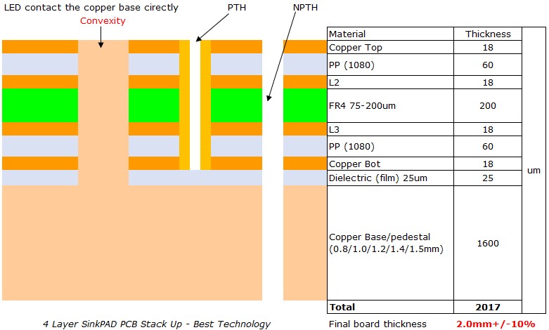
4 Layer SinkPAD Board on the Same Side

One common structure is the 4 layer SinkPAD board with four trace layers built on the same side of the copper base. This design allows engineers to place more traces in the same board size and create more complex layouts than with a 1 layer or 2 layer SinkPAD board.

This structure is useful when the design needs strong thermal performance but also requires increased circuit density on one side.

Common Structures of Multi-Layer SinkPAD Board

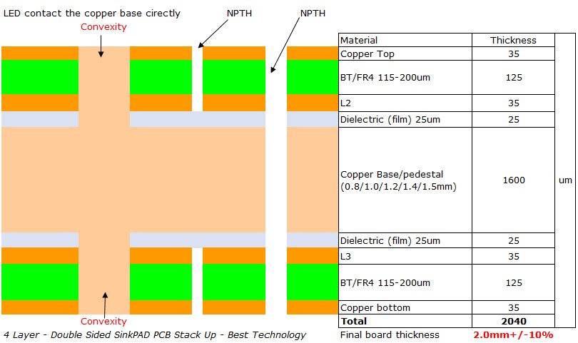
Double-Sided 4 Layer SinkPAD Board

Another option is the double-sided 4 layer SinkPAD board, where two trace layers are placed on the top side and two trace layers are placed on the bottom side. This structure increases usable routing area and supports more advanced product architectures.

However, this type of board is more difficult to design and manufacture. Since components may be mounted on both sides, engineers must carefully consider how heat will be transferred to the heatsink.

Common Structures of Multi-Layer SinkPAD Board

Design Considerations for Double-Sided Multi-Layer SinkPAD Board

A double-sided multi-layer SinkPAD board does not use plated through holes in the same way as traditional multi-layer metal core PCBs. This is due to process limitations in SinkPAD manufacturing. That also means the routing strategy, layer transition plan, and thermal structure need to be considered very carefully during design.

When engineers choose this structure, they usually need to evaluate:

  • Where the heatsink will be located
  • How heat will leave the copper base efficiently
  • Whether components on both sides will affect thermal transfer
  • How to maintain electrical routing without plated through holes
  • Whether the added layout complexity is justified by the application

Because of these design challenges, multi-layer SinkPAD boards are generally used only when simpler SinkPAD structures cannot meet the routing needs of the product.

Multi-Layer SinkPAD Board Applications

Multi-layer SinkPAD boards are mainly used in products that combine high heat generation with more complex circuit requirements.

Typical applications include:

  • High power LED modules up to 200W
  • High-power semiconductor devices
  • Power transistor circuits
  • Thyristor and diode modules
  • High-power resistor applications
  • Compact thermal management systems
  • Advanced lighting products with dense layout design

These boards are especially useful when product designers need to control heat effectively without giving up routing flexibility.

Multi-Layer SinkPAD Board Capability

ItemCapability
Base MaterialCopper
Copper Base Thickness1.2mm, 1.4mm, 1.5mm, 1.6mm
Thermal Conductivity400 W/m.K
Board Thickness1.6mm to 2.0mm
Copper Thickness0.5 oz, 1 oz, 2 oz, 3 oz
Outline ProcessingRouting, Punching, V-Cut
Solder Mask ColorWhite, Black, Blue, Green, Red
Silkscreen ColorBlack, White, Yellow
Surface FinishImmersion Gold, ENEPIG, Immersion Tin, OSP
Max Panel Size600 x 500mm
PackingVacuum packing, plastic bag
Sample Lead Time3 to 4 weeks
Mass Production Lead Time4 to 6 weeks

Why Choose a Multi-Layer SinkPAD Board?

A multi-layer SinkPAD board is a strong option when your product needs more than basic thermal management. It gives engineers more routing freedom while still preserving the direct thermal path needed for high-power components.

Compared with simpler SinkPAD structures, it supports more advanced circuit layouts. Compared with ordinary metal core PCB designs, it provides a more efficient thermal path. This makes it a practical solution for applications where both electrical complexity and thermal performance are important.

If your design requires compact size, high heat dissipation, and more circuit layers in the same board area, a multi-layer SinkPAD board can deliver clear advantages.

You may also like

2 Layer SinkPAD Board

March 24th, 2026

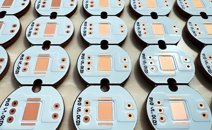
A 2 Layer SinkPAD board is a copper-based PCB structure designed for applications that need both strong thermal performance and more routing space on a compact layout. It features two circuit layers built on the same side of the board, combined with a dielectric insulation layer and a copper core or raised copper pedestal.

Unlike conventional metal core PCBs, the thermal pad of the LED in a 2 Layer SinkPAD board is placed directly on the copper core. This creates a direct thermal path, allowing heat to move away from the LED much faster. Because of this structure, the board is widely used in thermoelectric separation designs where electrical routing and thermal transfer need to be handled independently.

What Is a 2 Layer SinkPAD Board?

A 2 Layer SinkPAD board is a single-sided direct thermal path PCB with two copper trace layers arranged on the same side. Although it contains two routing layers, it is still considered a single-sided SinkPAD PCB because both circuit layers are located on the top side of the board.

The main advantage of this construction is that it combines electrical isolation with direct heat conduction. The circuit traces remain electrically insulated through the dielectric layer, while the LED thermal pad contacts the copper base directly.

Compared with a 1 Layer SinkPAD board, the 2-layer version supports more complex circuit routing on the same board size. That makes it a practical choice for compact, high-power lighting designs where both thermal control and circuit density matter.

2 Layer SinkPAD Board

2 Layer SinkPAD Board

How Does a 2 Layer SinkPAD Board Work?

The board works by separating the electrical path from the thermal path. Electrical signals move through the copper trace layers, while heat generated by the LED or power device is transferred directly into the copper core.

Since copper has very high thermal conductivity, around 400 W/m.K, heat can spread quickly from the hot spot to the base metal. From there, it can be transferred to a heatsink, mounting surface, or surrounding air. The direct contact design improves thermal efficiency far beyond what is possible with standard MCPCB structures. As a result, the LED junction temperature can be controlled more effectively.

Why Choose a 2 Layer SinkPAD Board Instead of a Standard MCPCB?

A standard metal core PCB usually includes a dielectric layer between the heat source and the metal base. That structure provides insulation, but it also adds thermal resistance. In a 2 Layer SinkPAD board, the thermal pad touches the copper pedestal directly, so heat does not need to pass through the dielectric in the same way.

This creates several practical benefits:

  • Lower thermal resistance
  • Better heat dissipation for high-power LEDs
  • More stable light output
  • Longer service life of the lamp
  • Higher routing density on the same board area
  • Better support for compact and advanced circuit design

For engineers working on high-power lighting modules, automotive lighting, or dense LED arrays, this structure offers a more efficient thermal solution without sacrificing design flexibility.

https://www.youtube.com/watch?v=KFQNdAvZGEA

Advantages of Using 2 layers SinkPAD Board

  • The metal core is Copper with high density, strong thermal carrying capacity and higher thermal conductivity. So the volume can be smaller under the same power.
  • It adopts the thermoelectric separation structure, the Lumens depreciation of the LED is minimized, and the life of the lamp is prolonged.
  • Suitable for matching single high-power lamp, such as Cree XPL, XML, XHP; Osram LED, etc., also COB package LED
  • High power semiconductors (transistors, thyristors, diodes) as well as resistors.
  • A variety of Surface Finishing are available according to different demands. (ENIG, OSP, Immersion Tin, ENEPIG, HAL) with excellent reliability of the surface treatment layer.
  • Different structures can be made according to different design needs of LED. (Such as copper bump, copper concave block)
  • Put more circuits on the same side, design more complicated circuit board.

Typical Applications of 2 Layer SinkPAD Board

A 2 Layer SinkPAD board is commonly used in products that require both strong thermal conductivity and compact circuit design.

Typical applications include:

  • High power LED modules up to 200W
  • COB LED lighting
  • Single high-power LEDs such as Cree XPL, XML, XHP, and Osram LEDs
  • Automotive lighting systems
  • Industrial lighting equipment
  • Power semiconductor modules
  • High-power resistor circuits
  • Thermoelectric separation applications

Because of its copper direct thermal path structure, this board is especially useful in lighting products where heat buildup directly affects brightness consistency and service life.

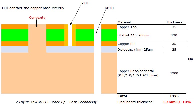
2 Layer SinkPAD Board Stack-Up

The typical stack-up of a 2 Layer SinkPAD board includes:

  • Two copper circuit trace layers on the same side
  • Dielectric insulation layer
  • Copper core or copper pedestal
  • Direct thermal contact area under the LED thermal pad
2 Layer SinkPAD Board Stack-Up

This stack-up is designed to achieve both electrical isolation and rapid heat transfer. It is one of the main reasons this board performs much better than ordinary aluminum PCB or traditional MCPCB in high thermal load applications.

Our 2 Layer SinkPAD Board Capability

ItemCapability
Base MaterialCopper
Copper Base Thickness0.8mm, 1.0mm, 1.2mm, 1.4mm, 1.5mm
Thermal Conductivity400 W/m.K
Board Thickness1.0mm to 2.0mm
Copper Thickness0.5 oz, 1 oz, 2 oz, special 3 to 10 oz
Outline ProcessingRouting, Punching, V-Cut
Solder Mask ColorWhite, Black, Blue, Green, Red
Silkscreen ColorBlack, White, Yellow
Surface FinishImmersion Gold, ENEPIG, Immersion Tin, OSP
Max Panel Size600 x 500mm
PackingVacuum packing, plastic bag
Sample Lead Time1.5 to 2 weeks
Mass Production Lead Time2 to 3 weeks

Why Is 2 Layer SinkPAD Board a Good Choice for High-Power LED Design?

In high-power LED products, heat is often the main factor that limits performance. Excessive temperature can reduce brightness, accelerate lumen depreciation, and shorten product lifespan. A 2 Layer SinkPAD board helps solve this issue by allowing heat to move directly into the copper base without unnecessary thermal barriers.

At the same time, the two-layer trace design gives more room for routing, which is useful when the LED module includes more complex circuitry. It is especially suitable for high-power LED modules, COB lighting, and power semiconductor applications where thermal performance directly affects reliability and lifespan. For projects that need both strong heat dissipation and more circuit freedom, a 2 Layer SinkPAD board is a highly effective choice.

FAQs about 2 Layer SinkPad MCPCB

1. What is a 2 Layer SinkPAD Board?

A 2 Layer SinkPAD Board is a high-power Metal Core PCB (MCPCB) that features two copper circuit layers on one side of a metal base. Unlike standard 2-layer MCPCBs where a dielectric layer separates all components from the metal core, the SinkPAD design “sinks” the thermal pad of a component through the dielectric, creating a Direct Thermal Path (DTP) to the copper or aluminum base.

2. How does a 2 Layer SinkPAD differ from a Single Layer SinkPAD?

While a single-layer SinkPAD only allows for simple circuit routing, a 2 Layer SinkPAD provides an additional copper layer for complex circuit design. This allows for more sophisticated power management, signal routing, or the placement of control components on the same board as high-power LEDs or transistors, all while maintaining the ultra-low thermal resistance of a direct-to-metal connection.

3. What are the thermal conductivity benefits of a 2 Layer SinkPAD?

Because the thermal pad of the component bypasses the 1–8 W/m·K dielectric layer and sits directly on the metal core, the effective thermal conductivity can reach 400 W/m·K (using a copper base). This is significantly higher than a standard 2-layer MCPCB, which is limited by the thermal resistance of the thin prepreg or dielectric layer required for circuit isolation.

4. Can I use Plated Through Vias (PTH) on a 2 Layer SinkPAD Board?

Yes, 2 Layer SinkPAD boards support inter-layer vias to connect the two copper circuit layers. However, these vias are typically used for electrical signals or low-power traces. The primary heat dissipation is still handled by the pedestal (the “SinkPAD”) that connects the high-power component’s thermal pad directly to the metal substrate, rather than relying on thermal vias.

5. When should I choose a 2 Layer SinkPAD over a standard FR4 with thermal vias?

You should choose a 2 Layer SinkPAD when your components generate heat that exceeds the capacity of FR4 (typically >3W per LED). While FR4 with thermal vias is cheaper, it cannot match the thermoelectric separation efficiency of a SinkPAD. If your application involves high-density power electronics where space is limited and active cooling is not an option, the 2-layer SinkPAD is the superior choice for reliability.

6. How does a 2 Layer SinkPAD differ from a Double-Sided SinkPAD PCB?

The primary difference lies in the circuit density versus mounting capability.

  • 2 Layer SinkPAD: Features two copper circuit layers (Top & Bottom) on one side of the metal base. It is designed for complex circuitry that requires more routing space or inter-layer connections (vias) while still maintaining a Direct Thermal Path (DTP) for high-power components on the top side.
  • Double-Sided SinkPAD: Features circuit layers and component mounting pads on both sides of the metal core (Top and Bottom). This allows you to mount high-power components, like LEDs or transistors, on both surfaces of the board, with each side utilizing the central metal core for heat dissipation.

You may also like

Double Sided SinkPAD Board

March 24th, 2026

What Double Sided SinkPAD Board is?

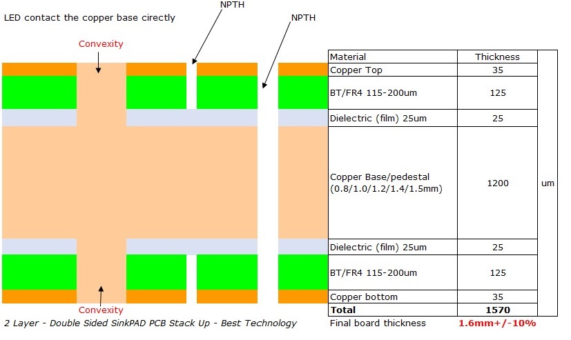
The Double sided SinkPAD board consists of at least two layers of trace circuit, and there’re at least one circuit layer on both top and bottom side of board, a dielectric (non-conducting) layer, a metal core/pedestal which normally is copper.

As there’re circuit layer on both sides, so engineer can put more (about 2 times, ideally) components on the same size circuit to realize more function, more complicated design, comparing to 1 Layer SinkPAD board or 2 layers SinkPAD board.

Double Sided SinkPAD Board

There’s no PTH (plated through hole) on double sided SinkPAD board, because the limitation of manufacturing process, which different from double sided Metal Core PCB which has a lot of PTH, and thermal PAD of LED will be put directly on copper core, also belonging to Direct Thermal Path (DTP) board too, but engineer needs to consider where the heat sink will be if he want more fast heat transferring, as there’re always components on both sides, and that make double sides SinkPAD board designing becoming more difficult & complex comparing to 1L SinkPAD board, or 2L SinkPAD board.

Stack up of Double Sided SinkPAD Board

Double Sided SinkPAD Board

Advantages of Utilizing Double Sided SinkPAD Board:

  • Put more components on the both top and bottom, design more complicated circuit board.
  • It adopts the thermoelectric separation structure, the Lumens depreciation of the LED is minimized, and the life of the lamp is prolonged.
  • Suitable for matching single high-power lamp, such as Cree XPL, XML, XHP; Osram LED, etc., also COB package LED
  • High power semiconductors (transistors, thyristors, diodes) as well as resistors.
  • A variety of Surface Finishing are available according to different demands. (ENIG, OSP, Immersion Tin, ENEPIG, HAL) with excellent reliability of the surface treatment layer.

Application of Double Sided SinkPAD Board

  • High Power LED (up to 200W).
  • High semiconductors (transistors, thyristors, diodes) as well as resistors.

2 Layer SinkaPAD Board Capability

  • Base material: Copper: 0.8mm, 1.0mm, 1.2mm, 1.4mm, 1.5mm
  • Thermal Conductivity: 400 W/m.K.
  • Board Thickness: 1.0mm~2.0 mm (0.04″~0.08″)
  • Copper thickness: 0.5 OZ, 1.0 OZ, 2.0 OZ (specially 3-10 OZ)
  • Outline: Routing, punching, V-Cut
  • Soldermask: White/Black/Blue/Green/Red Oil
  • Legend/Silkscreen Color: Black/White/Yellow
  • Surface finishing: Immersion Gold, ENEPIG, Immersion Tin, OSP
  • Max Panel size: 600*500mm(23.62″*19.68″)
  • Packing: Vacuum/Plastic bag
  • Samples L/T: 1.5~2 weeks
  • MP L/T: 2-3 weeks

Click here to see the manufacturing process of double sided SinkPAD Board and other options.

If you want to customize double sided SinkPAD board, please contact EBest Circuit (Best Technology) today send your request for double sides SinkPAD PCB.

FAQs about Double-Sided SinkPAD Boards

1. What is a Double-Sided SinkPAD Board and how does it work?

A Double-Sided SinkPAD Board is a specialized Metal Core PCB (MCPCB) that provides a Direct Thermal Path (DTP) on both sides of the board. Unlike standard MCPCBs that use a dielectric layer to separate the circuit from the metal base, SinkPAD technology removes the dielectric under the component’s thermal pad. This allows the component (like a high-power LED) to sit directly on the copper or aluminum core, drastically reducing thermal resistance.

2. How does a Double-Sided SinkPAD differ from a standard Double-Sided MCPCB?

The primary difference is the thermal conductivity. In a standard double-sided MCPCB, heat must travel through a thermally conductive dielectric layer (typically 1–8 W/m·K) to reach the metal core. In a SinkPAD board, the dielectric is bypassed entirely for the thermal pad, allowing for conductivity ratings as high as 400 W/m·K (if using a copper core). Additionally, double-sided SinkPADs allow for higher component density by utilizing both the top and bottom layers for active circuitry.

3. Why would I choose a double-sided design over a single-layer SinkPAD?

Engineers choose double-sided SinkPADs when they need to maximize functional density in compact spaces. It allows for roughly twice the component population or more complex circuit routing compared to a 1-layer board. This is ideal for high-power applications where you need to mount LEDs or transistors on one side while placing control circuitry, connectors, or additional power components on the other.

4. Are there limitations to the Plated Through Holes (PTH) in double-sided SinkPADs?

Yes. Due to the unique manufacturing process where the metal core is “sunk” or embossed to meet the trace layer, standard Plated Through Holes (PTH) are often limited or more complex to implement than in traditional FR4 boards. Connections between sides are typically handled through specialized routing or assembly techniques, so it is crucial to consult with your manufacturer during the design phase to ensure the layout is compatible with the “thermoelectric separation” structure.

5. Which base material is better for SinkPAD boards: Aluminum or Copper?

  • Copper: Best for ultra-high-power applications. It offers superior thermal conductivity (approx. 400 W/m·K) and is the most common choice for SinkPAD convexity because it is easier to etch and process for this specific technology.
  • Aluminum: More cost-effective and lighter. While it has good thermal properties, the chemical process for creating the SinkPAD convexity is more complex, often making it more expensive or difficult to produce than copper-based SinkPADs.

6. Can SinkPAD technology be used for components other than LEDs?

Absolutely. While most commonly used for high-power LEDs (Cree, Osram, etc.) to prevent lumen depreciation, SinkPAD boards are excellent for any high-power semiconductor that features an electrically neutral thermal pad. This includes power transistors, thyristors, diodes, and high-wattage resistors used in automotive, aerospace, or industrial power monitoring.

You may also like

Multi Layer Metal Core PCB

March 24th, 2026

Just like FR4 PCB, we can also make boards with more than 2 layers of traces and we named it “Multi Layers MCPCB“. The structure is similar with FR4 Multi Layers, but it much more complex to make.

You can populated more components on the boards, put signal and ground layer into seperated layers, to achieve better performance in electrical performance.

Compared with normal FR4, this sturcture need more technology and experience on laminating of more than two layers together with metal core and the cost is much higher than 2 layers MCPCB or double sided MCPCB.

Structure of Multi Layers MCPCB

Multi Layer Metal Core PCB

Capability of Multi Layers MCPCB

  • Base material: Aluminum/Copper/Iron Alloy
  • Thermal Conductivity (dielectrial layer): 0.8, 1.5, 2.0, 3.0 W/m.K.
  • Board Thickness: 0.8mm~3.0mm(0.02″~0.12″)
  • Copper thickness: 0.5 OZ, 1.0 OZ, 2.0 OZ, 3.0 OZ
  • Outline: Routing, punching, V-Cut
  • Soldermask: White/Black/Blue/Green/Red Oil
  • Legend/Silkscreen Color: Black/White
  • Surface finishing: Immersion Gold, HASL, OSP
  • Max Panel size: 600*500mm(23.62″*19.68″)
  • Packing: Vacuum/Plastic bag
  • Samples L/T: 15~18 Days
  • MP L/T: 15~20 Days

FAQs

1. What is a multi-layer MCPCB and how does it differ from standard FR4?

A multi-layer MCPCB consists of multiple copper conductive layers separated by high-thermal-conductivity dielectric layers, all bonded to a metal base (usually Aluminum or Copper). Unlike standard FR4, which relies on the epoxy glass substrate for structure, an MCPCB uses the metal base as a heat sink. While FR4 is an insulator with poor thermal management, the metal core in an MCPCB allows for heat dissipation rates that are significantly higher, making it essential for high-power electronics.

2. What are the typical thermal conductivity levels for multi-layer MCPCBs?

The thermal performance of a multi-layer MCPCB is primarily determined by the dielectric layer rather than the metal base itself. Standard dielectric materials offer conductivity between 1.0 W/mK and 3.0 W/mK. However, high-performance multi-layer stacks used in automotive or aerospace applications can reach 4.0 W/mK to 8.0 W/mK. Choosing the right dielectric is a balance between thermal efficiency and the breakdown voltage required for the circuit.

3. How many layers can be integrated into a Metal Core PCB?

Technically, “multi-layer” in the context of MCPCBs typically refers to 2-layer or 4-layer configurations. While it is possible to go higher, the complexity increases significantly because all heat must eventually pass through the dielectric layers to reach the metal base. In a 4-layer stack, the inner layers are further from the heat sink, which can lead to thermal bottlenecks if the design does not utilize thermal vias effectively.

4. Can you use plated through-holes (PTH) in a multi-layer MCPCB?

Yes, but the process is more complex than with standard PCBs. To prevent short-circuiting the signals to the metal core, the metal base must be pre-drilled and filled with an epoxy resin before the copper layers are laminated. Then, a smaller hole is drilled through the resin plug and plated. This creates an “insulated via” that allows signals to pass through the metal core safely.

5. What are the main applications for multi-layer MCPCB designs?

Multi-layer MCPCBs are the go-to solution when space is limited but power density is high. Common applications include:

  • Automotive: LED headlight systems and power converters (EV/HEV).
  • Power Supplies: High-voltage regulators and heavy-duty industrial rectifiers.
  • Aerospace: Power distribution units where weight and heat must be managed simultaneously.
  • Medical: High-intensity surgical lighting and imaging equipment.

6. What are the manufacturing challenges of multi-layer MCPCBs?

The primary challenge is coefficient of thermal expansion (CTE) mismatch. Metal bases (Aluminum/Copper) expand at different rates than the copper traces and dielectric during the lamination process. This can lead to delamination or bowing of the board. Precise control over the pressing cycle and the use of specialized “no-flow” or “low-flow” prepregs are required to ensure the structural integrity of the multi-layer stack.

You may also like

Double Sided Metal Core PCB

March 20th, 2026

A double sided metal core PCB also has same two layers of copper conductor like Double layers MCPCB, but the metal core is in the middle of two conductor, so there’re conductors (trace) on both sides of metal core, and were connected to each other by Vias. So we named it “Double sided MCPCB”, and you can populated SMD on both top and bottom.

Different with Single layer MCPCB, double sided MCPCB also requires an additional pressing step to laminate the imaged thermal conductive laminate and metal core (also known as metal base) together. But sometimes, some raw Metal Clad material vendor will supply board material which already laminated.

Compared with normal FR4, this structure need more technology and experience on laminating of two layers together with metal core.

Structure of Double Sided MCPCB

Structure of Double Sided MCPCB

Capability of Double Sided MCPCB

  • Base material: Aluminum/Copper/Iron Alloy
  • Thermal Conductivity (dielectric layer): 0.8, 1.5, 2.0, 3.0 W/m.K.
  • Board Thickness: 0.5mm~3.0mm (0.02″~0.12″)
  • Copper thickness: 0.5 OZ, 1.0 OZ, 2.0 OZ, 3.0 OZ, 4.0 OZ, 5.0 OZ
  • Outline: Routing, punching, V-Cut
  • Solder mask: White/Black/Blue/Green/Red Oil
  • Legend/Silkscreen Color: Black/White
  • Surface finishing: Immersion Gold, HASL, OSP
  • Max Panel size: 600*500mm (23.62″*19.68″)
  • Packing: Vacuum/Plastic bag
  • Samples L/T: 10~15 Days
  • MP L/T: 12~15 Days

FAQs about Double sided Metal Core PCB

1. What is a double-sided metal core PCB?

A double-sided MCPCB consists of two circuit layers (top and bottom) with a metal core—typically aluminum or copper—sandwiched in the middle. Unlike standard FR4 boards, the metal core acts as a high-efficiency heat sink. The layers are connected using insulated through-holes or thermal vias to ensure electrical signals pass through without shorting against the metal base.

2. How does a double-sided MCPCB differ from a single-sided one?

The primary difference lies in component density and routing complexity.

  • Single-Sided: Components are on one side; the metal base is on the back. It is simpler and cheaper but limited in space.
  • Double-Sided: Allows for components and traces on both sides of the metal core. This is necessary for complex designs where high power density requires cooling for components on both surfaces of the board.

3. What materials are used for the core in double-sided PCBs?

The three most common materials are:

  • Aluminum (6061 or 5052): The most cost-effective and popular choice, offering good thermal conductivity and mechanical stability.
  • Copper: Offers superior thermal conductivity (nearly double that of aluminum) but is significantly heavier and more expensive.
  • Stainless Steel: Used primarily for its mechanical strength and corrosion resistance, though its thermal performance is lower than aluminum.

4. Why are double-sided MCPCBs used instead of standard FR4?

Standard FR4 is a poor thermal conductor. In high-power applications, heat builds up and can cause component failure. Double-sided MCPCBs are used because the metal core can dissipate heat at rates of 1.0 W/mK to 9.0 W/mK (or higher), whereas FR4 typically manages only 0.25 W/mK. This allows for smaller form factors without overheating.

5. What are the main applications for double-sided metal core PCBs?

These boards are a staple in industries where heat management is critical:

  • Automotive: LED headlights, power converters, and motor control modules.
  • Lighting: High-output street lights and industrial floodlights.
  • Power Electronics: Solid-state relays, rectifiers, and high-capacity power supplies.
  • Telecommunications: Signal amplifiers and high-frequency filtering equipment.

6. What are the manufacturing challenges of double-sided MCPCBs?

The most significant challenge is the drilling and insulation process. Because the core is conductive metal, every through-hole must be pre-drilled, filled with a specialized dielectric resin, and then re-drilled to prevent the copper pins from touching the metal core. This requires high precision and specialized lamination techniques to ensure the board does not delaminate under thermal stress.

You may also like

COB MCPCB

March 20th, 2026

What is Chip On Board COB MCPCB?

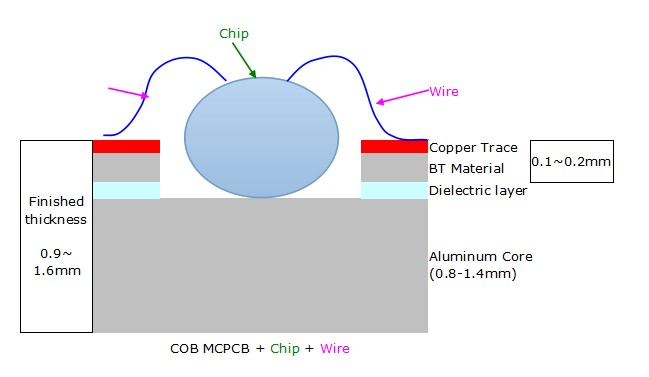
COB MCPCB, known as “Chip-On-Board” Metal Core PCB, is a type of MCPCB used in thermoelectric separation application. By using COB MCPCB, the micro-chip (also known as “die”) directly touch the metal core where the heat dissipate, and electrically interconnect the trace of circuit board (wire-bonding) so that power supply can be provided.

In normal MCPCB, there’s a dielectric layer between trace copper and metal core, and the thermal conductivity is limited by that dielectric layers, so value can only be 1~3 W/m.K. But using COB MCPCB, there’s no such dielectric layer because chip (die) direct touch the metal core, so thermal conductivity value of COB MCPCB will be almost the same one of metal core material itself. The normal material of metal core is aluminum, so thermal conduviity of COB MCPCB is more than 200W/m.K.

COB MCPCB

COB MCPCB (Chip on Board)

What are the COB Wire Bonding Processes?

COB process consists of three main categories to perform when manufacturing the Chip-on-Board:

1st: die mount or die attach;

2nd: wire bonding;

3rd: the encapsulation of die wires.

By using wire bonding & epoxy packaging then directly embedded on MCPCB, this practice can extend the lifespan of LED and unified light emission.

According to process and material, COB MCPCB applications can be categorized into two types: Mirror Aluminum and silver or gold platting aluminum, or silver plating mirror aluminum PCB.

Structure of COB MCPCB

Structure of COB MCPCB

Advantage of utilizing COB MCPCB

  • Excellent heat dissipation
  • High thermal conductivity: 137W/m.K
  • Higher reliability with better heat dispatch and small number of solder joint.
  • Provide enhanced reliability and lifespan of LED
  • Easy assembly for high powers LEDs
  • High quality material and production process allows easy assembly and substantial reduce the error percentage in assembly process
  • Substantially reduced space and cost
  • With better security protection (difficult to hack using reverse engineering)
  • Shorter time to the market

Application of COB MCPCB

  • High Power LED (up to 200W)
  • LED Backlight for LED TV
  • LED Front Light for E-Book
  • Agriculture & Horticulture Lighting
  • Street & Parking Lot Lighting
  • Automotive
  • Power Supply
  • ustomer Electronics Lighting
  • Other products that require thermal solutions
Application of COB MCPCB

FAQs about COB MCPCBs

1. What is the difference between a standard MCPCB and a COB MCPCB?

A standard MCPCB (Metal Core PCB) usually has SMT (Surface Mount Technology) components soldered onto a dielectric layer. In contrast, a COB (Chip-on-Board) MCPCB allows the LED semiconductor chip to be mounted directly onto the metal core or into a recessed “well.” This removes the thermal resistance of the LED package itself, allowing for much higher power density.

2. Why is thermal conductivity so important for COB MCPCBs?

Since COB LEDs pack many light-emitting diodes into a very small area, they generate intense localized heat. If this heat isn’t dissipated, the LED’s lifespan and brightness (luminous flux) drop rapidly. COB MCPCBs use materials like Aluminum or Copper to pull heat away from the chips at rates significantly higher than standard FR4 boards.

3. What are the common base materials used in COB MCPCBs?

  • Aluminum: The most common and cost-effective choice for general lighting.
  • Copper: Offers superior thermal conductivity but is heavier and more expensive; used for extreme high-power applications.
  • Stainless Steel: Occasionally used for high-strength requirements, though it has poorer thermal properties than Aluminum.

4. What is a “Mirror Aluminum” COB MCPCB?

A Mirror Aluminum COB MCPCB features a highly reflective, polished surface. This design ensures that light emitted from the sides of the LED chips is reflected forward, increasing the overall light output efficiency (Lumen/Watt) by reducing light absorption by the board itself.

5. Can COB MCPCBs be used with high-voltage applications?

Yes, but they require a specialized dielectric layer. This layer must be thin enough to allow heat to pass through to the metal core, but thick enough to provide electrical insulation (dielectric breakdown voltage) to prevent short circuits, especially in AC-driven LED modules.

6. What are the main applications for COB MCPCB technology?

Because they offer high brightness in a compact footprint, they are the industry standard for:

  • Automotive lighting (Headlights).
  • Industrial high-bay lighting.
  • Street lights and architectural floodlights.
  • Commercial downlights and track lighting.

You may also like

Single Layer MCPCB

March 20th, 2026

A simple layer single sided MCPCB consists of a metal base (usually aluminum, or copper alloy), Dielectric (non-conducting) Layer, Copper Circuit Layer, IC components and solder mask.

The prepreg dielectric provides excellent heat transfer from the foil and components to the base plate, while maintaining excellent electrical isolation. The base aluminum/copper plate gives the single-sided substrate mechanical integrity, and distributes and transfers the heat to a heat sink, mounting surface or directly to the ambient air.

The Single-Layer MCPCB can be used with surface mount and chip & wire components, and provides much lower thermal resistance than FR4 PWB. The metal core provides lower cost than ceramic substrates, and allows much larger areas than ceramic substrates.

Single Layer MCPCB

Single Layer MCPCB Capability

  • Base material: Aluminum/Copper/Iron Alloy
  • Thermal Conductivity (dielectrial layer): 0.8, 1.0, 1.5, 2.0, 3.0 W/m.K.
  • Board Thickness: 0.5mm~3.0mm(0.02″~0.12″)
  • Copper thickness: 0.5 OZ, 1.0 OZ, 2.0 OZ, 3.0 OZ, up to 10 OZ
  • Outline: Routing, punching, V-Cut
  • Soldermask: White/Black/Blue/Green/Red Oil
  • Legend/Silkscreen Color: Black/White
  • Surface finishing: Immersion Gold, HASL, OSP
  • Max Panel size: 600*500mm(23.62″*19.68″)
  • Packing: Vacuum/Plastic bag
  • Samples L/T: 4~6 Days
  • MP L/T: 5~7 Days

Single Layer MCPCB FAQs

1. What is a single layer MCPCB?

A single layer MCPCB consists of a metal base (typically aluminum or copper), a non-conductive dielectric layer, and a copper circuit layer. Unlike standard PCBs, the metal core acts as a primary heat sink, moving thermal energy away from high-power components to the environment or an external cooling system.

2. How does a single layer MCPCB differ from a standard FR4 PCB?

The primary difference is the substrate material. While FR4 uses fiberglass and epoxy, an MCPCB uses a metal base. This allows MCPCBs to have significantly higher thermal conductivity. While a standard FR4 board typically has a conductivity of around 0.25 W/mK, a single layer MCPCB can range from 1.0 W/mK to 9.0 W/mK depending on the dielectric material used.

3. What are the typical applications for single layer MCPCBs?

Single layer MCPCBs are most commonly used in the LED lighting industry (street lights, automotive headlamps, and backlight units) because LEDs generate significant heat that can degrade performance if not dissipated. They are also widely used in power conversion, solid-state relays, and the automotive sector for motor control modules.

4. Can you have plated through-holes (PTH) on a single layer MCPCB?

Generally, no. In a standard single layer MCPCB, the metal base is conductive, so through-holes would cause a short circuit between the signal layer and the base. Components are typically Surface Mount Devices (SMD). If through-hole components are required, specialized “COB” (Chip on Board) or complex insulated hole processes are needed, which significantly increases cost.

5. What are the layers of a single layer MCPCB?

A standard stack-up includes four main layers:

  • Solder Mask: Protects the copper circuit.
  • Circuit Layer: The copper foil used for traces.
  • Dielectric Layer: The most critical part; it provides electrical insulation while facilitating heat transfer.
  • Metal Substrate: Usually 1.0mm to 3.2mm of Aluminum (5052 or 6061) or Copper.

6. Is aluminum or copper better for the metal core?

Aluminum is the most popular choice because it is cost-effective and provides excellent thermal dissipation for most applications. Copper offers even higher thermal conductivity but is much heavier and more expensive. Copper is usually reserved for extremely high-power density applications where aluminum’s performance is insufficient.

You may also like