PCB manufacturing PCB manufacturing
Home > Blog

PCB Sourcing

How to Choose a Heavy Copper PCB Manufacturer in Europe (EU): Capabilities, Quality, and Cost
Thursday, September 17th, 2026

Choosing a heavy copper PCB manufacturer in Europe takes more than comparing a maximum copper figure, a European office address, or a row of certification logos. A supplier that advertises 10 oz or 20 oz copper may still be unable to hold your required spacing, plate your hole structure, or reproduce the approved prototype in volume.

This guide shows you how to compare the complete construction, quality evidence, certification coverage, manufacturing location, lead time, and delivered cost on an equivalent basis. The supplier with the longest capability list or lowest unit price is not always the best fit; the stronger choice is the one that can prove your exact board is buildable, controlled, and deliverable on the terms your project needs.

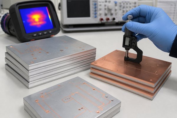
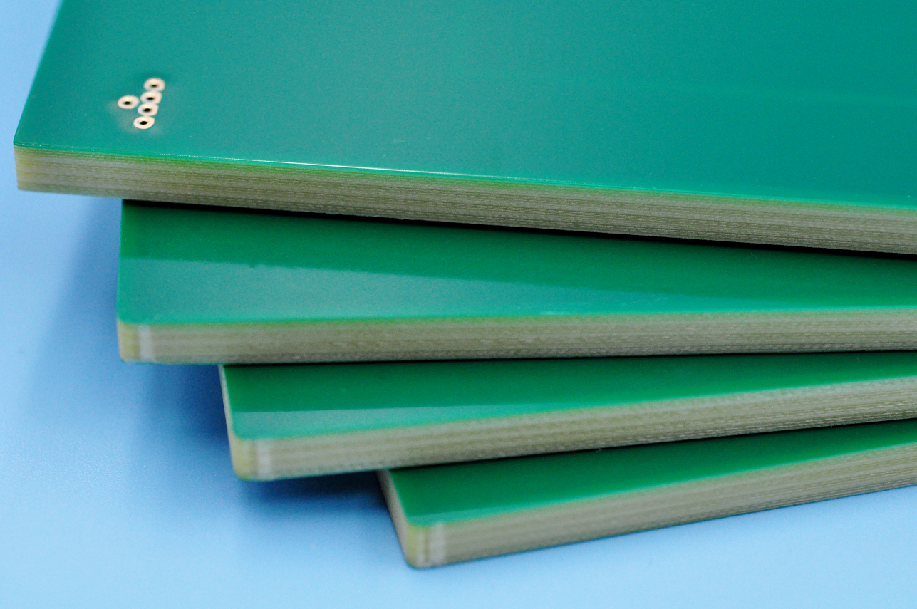
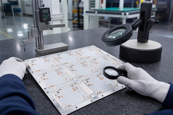
Heavy copper PCB manufacturer in Europe capability and quality inspection

What Should You Look for When Choosing a Heavy Copper PCB Manufacturer in Europe?

Start with the complete board construction and evidence from comparable production. These seven checks quickly separate a suitable factory from one relying on a maximum-copper figure or certification logos.

  1. Copper capability at your geometry. ā€œUp to 10 ozā€ says nothing about the spacing the factory can hold at 10 oz. Your comparison needs the finished copper on each layer, the line width and spacing at that thickness, and any difference between inner- and outer-layer limits.
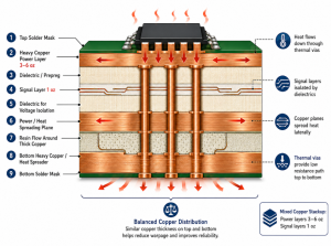
  2. Multilayer construction experience. A plant that makes a 6 oz double-sided board may not be able to build an eight-layer 6 oz stackup. Copper distribution, dielectric thickness, resin flow, lamination, overall thickness, and warpage all interact in a multilayer build.
  3. Hole and plating fit. Finished hole size, aspect ratio, annular ring, hole-wall copper, and via current duty belong in the same engineering conversation. Thick outer copper does not, by itself, prove adequate copper in the plated hole barrel.
  4. Evidence from a comparable job. A polished sample with a different layer count and copper weight has limited value. Microsections, copper measurements, electrical-test records, dimensional reports, and lot traceability are more useful when the previous build resembles your copper, geometry, and hole structure.
  5. Certificates tied to the factory. The document needs to cover the facility and activity involved in your order. A certificate held by a sales office, another group company, or an assembly plant does not automatically cover PCB fabrication.
  6. Continuity from prototype to production. Find out whether volume boards will use the same site, material, stackup, and approved process as the prototype. An attractive first build loses much of its value if production can move or change without notice.
  7. Real schedule and delivered cost. Factory days and unit price are only part of the decision. Engineering approval, material availability, inspection, transport, customs, freight, duties where applicable, and incoming handling can change which offer is genuinely faster or less expensive.

How Do You Compare Heavy Copper PCB Manufacturing Capabilities?

Compare copper thickness together with geometry, layer count, holes, material, and finishing. A maximum value taken from a capability chart cannot tell you whether the factory can manufacture the combination shown in your data.

Consider two suppliers. Supplier A promotes 10 oz copper but needs wider spacing at that thickness. Supplier B lists 6 oz as its practical limit and can hold your actual 6 oz traces, clearances, and finished holes. For a 6 oz design, Supplier B may be the closer technical match.

Design Requirement What to Compare Why It Matters
Copper and geometry Finished copper by layer with line width, spacing, and tolerance Etching becomes less forgiving as copper gets thicker; a limit achieved on wide features may not apply to tighter geometry.
Layer count and distribution Copper balance, dielectric thickness, resin fill, press cycles, and finished thickness Uneven copper and high thermal mass can affect resin flow, dimensional stability, and warpage.
Holes and plating Finished hole, aspect ratio, annular ring, barrel copper, and outer-layer buildup Smaller holes become harder to plate and finish when the surrounding copper construction is demanding.
Solder mask and finish Mask coverage, dams, clearances, application method, and surface finish The raised conductor profile can challenge mask coverage and leave less room between adjacent features.
Material and temperature Material properties, operating environment, thermal cycling, and copper expansion effects A manufacturable board still needs a material system suited to its electrical, thermal, and reliability conditions.

How Can You Verify a Manufacturer's Heavy Copper PCB Quality?

Use evidence that answers a specific risk in your board. Check what each record proves, how it was sampled, and whether it represents a comparable construction, rather than accepting a general claim that the factory performs inspection.

Evidence What It Can Show Limitation
Microsection Local layer copper, hole-wall plating, lamination condition, and visible voids It examines selected locations; it does not describe every feature on every board.
Copper measurement Whether sampled finished copper meets the stated target or minimum Results are meaningful only when the method, location, tolerance, and sampling plan are known.
AOI record Pattern inspection for conductor defects on the applicable layers AOI does not replace electrical test or prove internal plating quality.
Electrical test Continuity and isolation against the released net data It does not establish copper thickness, dimensional accuracy, or long-term thermal reliability.
Dimensional report Measured holes, outline, thickness, and drawing-controlled dimensions Its value depends on the reported features, acceptance limits, and sampling level.
Lot traceability Links among material batches, production lots, inspections, and shipped boards A trace code is useful only if the underlying records are retained and retrievable.

The copper result also needs a clear reference point: nominal or minimum, base or finished, inner or outer layer. These distinctions prevent a drawing requirement and a report value from sounding identical when they are not.

A well-made 4 oz sample does not prove capability for an eight-layer 8 oz board. Evidence from a similar copper weight, stackup, geometry, and hole structure gives a much stronger view of production readiness.

Which Certifications Matter for a Heavy Copper PCB Manufacturer in Europe?

  • ISO 9001: Use it as a general quality-management baseline. The certificate should name the facility involved in your order and include relevant PCB manufacturing activities in its scope.
  • IATF 16949, ISO 13485, or AS9100D: Match the certification to the end market and contract. Automotive, medical, and aerospace requirements are not interchangeable, and the quoted fabrication site must be covered.
  • UL recognition: Check whether the applicable material system, product category, and construction are covered. A supplier logo alone does not establish that your quoted board falls within the recognition.
  • RoHS and REACH: Treat these as product and material compliance requirements, not quality-management certificates. The declaration, material data, revision, and product coverage should match the board and destination market.
  • Site, scope, and validity: The company name, address, certified activities, and expiry date must apply to the factory doing the work. A certificate for a sales office, another group site, or an assembly plant does not cover PCB fabrication automatically.

Does Your Heavy Copper PCB Need to Be Manufactured in Europe?

Not necessarily. Delivery to Europe and manufacturing in Europe are different requirements, and many projects can use an overseas factory when the technical, documentation, and supply-chain conditions are acceptable.

European fabrication may be required by a customer-approved source list, a contract, a controlled program, an internal sourcing policy, or a regional supply mandate. In that situation, the order documents should identify the permitted facility rather than relying on the supplier's registered address.

Overseas production may remain a practical option when there is no location restriction, the board fits the factory's processes, the quality records meet the project need, and the team can manage transport and import risk. Local sales or engineering support can be useful, but it does not change where fabrication takes place.

Choose the production region from the project constraint first. Then compare the actual plant, technical fit, production controls, delivery route, and total cost within the options that remain.

What Determines Heavy Copper PCB Lead Time in Europe?

There is no dependable standard lead time for heavy copper boards. The schedule changes with the copper weight, material availability, layer count, lamination cycles, plating demand, line and spacing, hole structure, test plan, quantity, and first-article needs.

The starting milestone can change the apparent result. One quote may count from purchase order receipt, another from completed engineering review, and a third from material availability or stackup approval. A five-day difference on paper may disappear once both schedules start at the same event.

Door-to-door time adds the steps outside fabrication: engineering questions, document approval, packing, transport, customs clearance where applicable, local delivery, and incoming inspection. A nearby factory may shorten logistics, while a well-planned overseas route may still fit a stable production schedule.

Compare dates only after the starting event, factory completion event, shipment method, destination, and approval assumptions are aligned.

Why Do Heavy Copper PCB Prices Vary So Much Between Manufacturers?

Two suppliers can quote the same ā€œ6 oz PCBā€ at very different prices because they may not be quoting the same build. One may be pricing 6 oz finished copper with tight spacing and a full inspection package; the other may be working from a different starting copper, stackup, or test assumption.

  • Copper and process time: Heavy copper affects etching, plating, cycle time, process margin, panel utilization, and yield, not just the amount of raw copper.
  • Geometry: A 6 oz layout with generous spacing does not carry the same manufacturing risk as 6 oz around tighter conductors and clearances.
  • Layers and lamination: A double-sided power board and an eight-layer heavy copper build differ sharply in materials, press work, registration, and yield exposure.
  • Testing and records: Microsections, dimensional reports, first-article inspection, special traceability, or customer-specific documentation add work that may or may not be included.
  • Logistics: Freight, insurance, customs services, duties where applicable, local delivery, and incoming handling all affect the cost at the receiving dock.

For example, a €40 board quoted without freight, import charges, or extra inspection can cost more on arrival than a €46 board with a broader delivery and documentation package. Price becomes comparable only after the construction and included services are comparable.

What Should You Send Manufacturers to Get Comparable Quotes?

Send enough information for every factory to price the same board. Gerber files alone rarely settle the meaning of copper, material, tolerances, inspection, or delivery.

  • Design files: Gerber or ODB++, drill data, fabrication drawing, netlist when available, and one clearly identified revision.
  • Stackup: Layer count, board thickness, material or required properties, dielectric structure, and finished copper for each relevant layer.
  • Critical geometry: Minimum line and spacing, finished holes, tolerances, annular-ring concerns, and required plated-hole copper where specified.
  • Quality needs: Electrical test, microsection or cross-section needs, dimensional inspection, first-article records, traceability, and any customer-specific documents.
  • Order details: Prototype and production quantities, expected lot sizes, delivery destination, target arrival date, and any fixed manufacturing-location condition.

If suppliers work from different technical assumptions, their prices cannot be compared fairly. Proposed material or stackup changes should appear clearly beside the offer, not emerge after the order is placed.

How Should You Compare Heavy Copper PCB Quotes?

Compare five items before looking at the final number: finished copper, stackup and material, inspection, lead-time definition, and delivery coverage. A difference in any one of them can create a price gap that has nothing to do with manufacturing efficiency.

Quote Item What Must Match What Can Distort the Comparison
Finished copper Layer-by-layer value, minimum or nominal requirement, and tolerance Base copper presented as though it were the finished requirement
Stackup and material Approved construction, overall thickness, and required material properties An undisclosed equivalent, altered dielectric, or different press construction
Inspection Test coverage, sampling, reports, and traceability deliverables Special records priced separately or omitted
Lead time Starting milestone, completion milestone, approvals, and quantity Factory days compared with door-to-door time
Delivery Destination, freight, customs responsibility, and other included charges Different delivery terms or an incomplete landed-cost view

The lowest number is not the lowest-cost equivalent build when the assumptions differ. Resolve the technical and delivery differences first; the remaining price comparison will be far more useful.

What Are the Most Common Mistakes When Choosing a Heavy Copper PCB Manufacturer?

Most poor selections begin with a shortcut: one impressive number, one attractive sample, or one low price is allowed to stand in for the complete build. Six mistakes deserve particular attention.

  • Choosing by maximum copper thickness. The advertised limit may apply only to wider features or a simpler construction than yours.
  • Mixing base copper and finished copper. The same ā€œ6 ozā€ description can lead to different process plans when the measurement point is not stated.
  • Ignoring geometry at the target copper. Line width, spacing, holes, and annular rings can rule out a build even when the nominal copper is within range.
  • Assuming a European office means European fabrication. Sales, engineering, warehousing, and board production may occur in different countries.
  • Comparing unit prices built on different assumptions. Material substitutions, inspection exclusions, and delivery terms can make the cheapest line item the more expensive order.
  • Approving a prototype without controlling later changes. A move to another plant, material, stackup, or process can break the link between the approved sample and the production board.

FAQs About Choosing a Heavy Copper PCB Manufacturer in Europe

Q1. How do I know whether a supplier's 10 oz capability applies to my design?

A1. Compare the 10 oz claim with your minimum line and spacing, finished holes, layer count, total board thickness, and material. Ask for a written DFM response tied to the current data revision, not a general capability chart.

Q2. Should finished copper be specified separately for inner and outer layers?

A2. Yes. Outer layers can gain copper during through-hole plating, while inner layers follow a different process route. State the finished requirement for each relevant layer and identify whether the value is nominal or minimum.

Q3. What evidence should I request before approving a heavy copper prototype?

A3. Ask for a microsection, copper-thickness results, electrical-test record, critical dimensional results, and lot traceability when those records matter to the design. The evidence should come from your build or a genuinely comparable construction.

Q4. Can the prototype and production order use different factories?

A4. They can, but the change needs explicit review and approval. If continuity matters, require the same build site, approved material, stackup, and process route, plus written notification before any production change.

Q5. Do PCBs delivered to Europe have to be manufactured in Europe?

A5. No, unless a contract, customer approval, program rule, or sourcing policy sets a location condition. Boards made elsewhere can be supplied to Europe when the technical, compliance, import, and delivery requirements are met.

Q6. When does the quoted heavy copper PCB lead time start?

A6. It depends on the supplier. The clock may start at purchase order receipt, engineering approval, stackup approval, or material availability, so the quotation should name the starting milestone and the promised completion or arrival event.

Q7. Why can two 6 oz heavy copper PCB quotes differ so much?

A7. The suppliers may be using different definitions for finished copper, geometry, stackup, material, inspection, yield allowance, freight, or import responsibility. Align those assumptions before treating the price gap as a true manufacturing-cost difference.

Q8. What should I send for an accurate heavy copper PCB quotation?

A8. Send Gerber or ODB++, drill data, fabrication drawing, stackup, finished copper by layer, critical line and spacing, finished holes and tolerances, material requirements, quantities, inspection needs, revision, and delivery destination.

Planning a heavy copper PCB for a European project? Send your design files, stackup, finished copper requirements, quantities, inspection needs, and delivery destination to sales@bestpcbs.com for a construction-specific quotation.
You may also like

HDI PCB Manufacturers in Germany: 10 PCB Manufacturing Companies to Compare
Monday, September 7th, 2026

An RFQ sent to several HDI PCB manufacturers in Germany can return offers based on very different production routes. One supplier may fabricate the board at a named German plant; another may handle engineering or prototypes in Germany and use capacity elsewhere in Europe or Asia for series production. The production site affects stackup approval, process ownership, delivery planning and the work required if the build later moves.

Decide first whether the program needs a German-built prototype, continuing German production or a planned move to an overseas series plant. Then give every candidate the same stackup, via map, materials, quantities and required ship date. That produces a fairer comparison of capability, lead time and total sourcing risk.

HDI PCB Manufacturers in Germany, illustrative HDI bare board under optical inspection with a German flag

Compare 10 HDI PCB Manufacturers in Germany

German production is decisive for some projects; prototype speed, rigid-flex integration or a planned transfer to Asian volume may matter more for others. Compare these HDI PCB manufacturers in Germany by address, process limits, stated lead time and advantage to find the companies that fit the required production route.

Manufacturer German Address HDI Process Capability Lead Time Advantages
KSG GmbH Auerbacher Strasse 3–5
09390 Gornsdorf
75 µm line/space; laser microvias, buried vias, stacked and staggered structures 30 working days Company-owned HDI production in Germany and Austria
CONTAG AG PƤwesiner Weg 30
13581 Berlin
≤150 µm microvias and ≤100 µm structures; resin plugging and copper filling 3 working days; from 14 hours Very short prototype cycles from its Berlin plant
Unimicron Germany GmbH Am HollƤnder See 70
47608 Geldern
10-layer HDI example; filled and capped blind-via options By quotation German high-tech fab with access to group capacity in Asia
Würth Elektronik Circuit Board Technology Salzstrasse 21
74676 Niedernhall
MICROVIA.hdi, SLIM.hdi and ADVANCED.hdi; standard and custom buildups From 2 working days Strong design resources and standardized HDI technology families
Schweizer Electronic AG Einsteinstrasse 10
78713 Schramberg
Single, staggered, stacked and skipped microvias; hybrid HDI combinations By quotation HDI integration with automotive, RF and thermal technologies
Schaltungsdruck Storz Carl-Benz-Strasse 1
79341 Kenzingen
Up to 12 layers; 100 µm line/space and laser microvias ≄80 µm; more layers on request By quotation German manufacture with a managed partner route for selected series
ILFA GmbH Lohweg 3
30559 Hannover
50 µm laser-via example; blind, buried and stacked vias plus microfine structures By quotation Fine-feature engineering and in-house analytical capability
Kubatronik Leiterplatten GmbH Karl-Benz-Strasse 13
73312 Geislingen/Steige
75 µm line/space; blind, buried, stacked and staggered vias, via-in-pad and rigid-flex HDI By quotation HDI combined with flex and rigid-flex in German production
hmp HEIDENHAIN-MICROPRINT GmbH Rhinstraße 134
12681 Berlin
Up to 4+x+4; 75–150 µm laser blind holes, 75/75 µm line/space and microvia filling By quotation Specific published limits supported by broad in-house testing
Leiton GmbH Wolframstrasse 96
12105 Berlin
Structures to 75 µm; high-layer HDI exposure and German/Asian production routes From 2 working days German prototypes with managed transfer to China for series production

KSG GmbH

KSG owns two HDI production sites: Gornsdorf in Germany and Gars am Kamp in Austria. Its published SBU capability includes 75 µm line/space, laser-drilled microvias, buried vias and stacked or staggered structures. Projects that require German origin should name Gornsdorf in the quotation; projects that permit either European site can also be considered for the Austrian plant.

The two-site model gives buyers a company-owned European alternative when German origin is not mandatory. If origin or qualification is controlled, the quotation should name the approved plant and state whether a move between Gornsdorf and Gars am Kamp would change the laminate, stackup, inspection plan or qualification record.

CONTAG AG

CONTAG’s Berlin plant is geared to short-cycle HDI prototyping. It publishes HDI/SBU production with microvias at or below 150 µm, conductor structures at or below 100 µm, resin plugging and in-house copper filling.

Standard service begins at three working days, while the multilayer Blitz service begins at 14 hours for eligible builds. Those lead times are most relevant during fast layout or test iterations. Express eligibility still depends on the via pairs, filling, materials and impedance targets in the proposed construction.

Unimicron Germany GmbH

Unimicron Germany pairs its Geldern high-tech plant with the wider group’s Asian capacity. The German operation publishes HDI production for samples, small and medium lots, and higher quantities; its documented work includes a 10-layer HDI example and filled or capped blind-via options.

The mixed footprint may suit a program that wants German development production and a possible group route to higher volume. The plants are not automatically interchangeable: the quotation should name the prototype and series sites and identify any change in laminate, buildup, panel format or test plan before the stackup is released.

Würth Elektronik Circuit Board Technology

Würth Elektronik publishes a detailed set of HDI planning resources. MICROVIA.hdi, SLIM.hdi and ADVANCED.hdi are supported by standard stackups, digital stackup files, design rules and impedance guidance.

Those resources are useful before the RFQ: a layout team can begin with a documented buildup and see where a custom impedance stackup is needed. Eligible online-shop boards are advertised from two working days, although the chosen HDI family and production site determine the actual route.

Schweizer Electronic AG

Schweizer combines microvia HDI with RF, thermal and automotive technologies. Its portfolio covers single, staggered, stacked and skipped microvias, along with buried and mechanically drilled connections.

Development and PCB production are both present at Schramberg. That combination is especially relevant for boards where dense digital escape is only one part of the job—for example, an RF section or a thermally demanding power area on the same PCB. The quoted buildup and production location define which parts of the wider technology portfolio apply.

Schaltungsdruck Storz

Storz combines in-house production in Kenzingen with qualified Asian partners for selected series work. Its German capability includes complex multilayers, HDI and microvia technology up to 12 layers, 100 µm line/space and laser microvias from 80 µm.

Storz also describes samples made under series conditions. This is useful when the first build must represent the later process rather than serve as a one-off demonstrator. Buyers can keep German production where origin or process control requires it, or evaluate the managed Asian route for suitable volumes.

ILFA GmbH

ILFA publishes a 50 µm laser-via example and discusses the registration challenge behind very small target pads. The Hannover manufacturer’s wider scope includes blind, buried and stacked vias, microfine structures and in-house laboratory analysis.

Its fine-via work and laboratory capability address tight BGA escape regions and stacked microvias, particularly when drilling-to-pad registration drives feasibility. The 50 µm figure is a documented example; usable dimensions still depend on the complete copper and dielectric construction.

Kubatronik Leiterplatten GmbH

Kubatronik combines HDI/SBU with flex and rigid-flex manufacturing in Germany. Its published scope includes 75 µm line/space, blind, buried, stacked and staggered vias, via-in-pad and rigid-flex constructions with HDI layers. The company focuses on prototypes and low-to-medium volumes, addressing compact products that need dense component escape and a flexible interconnect in one construction.

For a rigid-flex HDI design, the complete construction needs one review rather than separate approvals for the dense rigid area and the flex tail. Microvia layer pairs, the rigid-to-flex transition, bend areas, coverlay openings and assembly clearances must work together; the published 75 µm line/space figure alone does not establish feasibility.

hmp HEIDENHAIN-MICROPRINT GmbH

hmp publishes concrete dimensions for its Berlin HDI process. The listed range covers SBU constructions up to 4+x+4, microvia filling, 75–150 µm laser-drilled blind holes and 75/75 µm line/space.

The published dimensions provide a starting range for an industrial board, supported by broad in-house testing. A design that approaches several limits at once still needs a complete stackup review because copper thickness, board thickness, material and via aspect ratio interact.

Leiton GmbH

Leiton links German prototype engineering with series production in China. Its Berlin headquarters handles inquiries, CAM preparation and technical clarification. Published services start at two working days, with 4–8-layer boards from three working days where the construction qualifies.

For a program that expects overseas volume, the series plant should review the stackup, blind-via arrangement and material family before the prototype layout is frozen. That review exposes geometry or material changes before the transfer becomes a second design cycle.

Comparison Criteria for German HDI PCB Manufacturers

Two quotations are comparable only when they describe the same board, production route and delivery point. Review each supplier against the following items before building a shortlist.

  • Fabrication route: identify the plant for prototypes and the intended plant for repeat orders. Record any partner route, transfer point and country-of-origin restriction, then require approval before the named route changes.
  • Accepted stackup and via map: submit the laser-via layer pairs, sequential-lamination cycles, buried vias, stacked or staggered connections and filled or capped via-in-pad requirements. The useful output is an approved buildup, not a general statement that HDI is available.
  • Combined process window: obtain approval for line/space, laser-via diameter, capture pad, copper weight, dielectric thickness and finished board thickness together. Isolated published minima may not be available in one construction.
  • Materials and impedance: agree the laminate family, copper, dielectric thicknesses, impedance targets, tolerances and coupon plan. List permitted equivalents and define which substitutions require customer approval.
  • Prototype-to-series continuity: when production may move, compare the material system, geometry, panel format and inspection plan before layout release. State what must be revalidated on the first build from the second plant.
  • Inspection and reliability evidence: select microsections, continuity checks, thermal stress or cycling, via-fill inspection and lot records according to the product risk. The quotation should name the included records and acceptance criteria.
  • Lead-time basis and capacity: compare the same quantity, finish, test scope and delivery point. Confirm when the clock starts, whether the date means factory completion or shipment, and whether repeat-order capacity differs from prototype capacity.
  • Commercial scope: compare tooling or NRE, test reports, packaging, freight terms and quotation exclusions on the same basis. A lower total is meaningful only when the accepted construction and included services are the same.

Why Choose EBest Circuit for Overseas HDI Production?

When German origin is not mandatory, EBest Circuit can quote a China-based HDI production route and review the build before release. The customer can settle the following points before placing the order:

  • Earlier DFM decisions: the proposed stackup, laser-via pairs, line/space, copper, materials and impedance targets are reviewed before release. The free DFM report records requested changes and open questions before fabrication.
  • One reviewed HDI construction: multilayer HDI PCB fabrication, laser microvias, stacked or staggered structures, via-in-pad and impedance control are assessed as one buildup rather than as unrelated capability limits.
  • Bare boards and assembly in one RFQ: optional PCB assembly allows the quotation to cover both stages. Add the BOM, placement data, approved substitutions and test requirements so the customer can compare the complete scope with a bare-board-only offer.
  • Prototype-to-repeat planning: quantities, target dates and the intended repeat-order route can be reviewed with the initial build. This gives the customer a chance to resolve material, panel and test-plan differences before they affect later orders.
  • Controlled second-source comparison: EBest’s proposed material system, geometry, panelization and impedance plan can be checked against a released German build before a transfer decision is made.
  • A quotation tied to the actual job: the accepted buildup, quantity, delivery destination, inspection scope and open technical items can be stated together, making supplier offers easier to compare on the same basis.

FAQs About HDI PCB Manufacturers in Germany

Q1: Which files are needed for a comparable HDI PCB quotation?

A1: Send the same revision of the Gerber or ODB++ data, fabrication drawing, stackup, via map, materials, copper weights, finished thickness and tolerances, impedance targets, surface finish, test scope, quantity, destination and required ship date to every supplier.

Q2: How can a buyer verify that the quoted boards will be fabricated in Germany?

A2: Require the quotation and order acknowledgement to name the fabrication plant. If German origin is mandatory, put it in the purchase requirements and prohibit subcontracting or plant changes without approval.

Q3: Which HDI process limits must be approved as a combination?

A3: Approve line/space, laser-via and capture-pad diameters, copper weight, dielectric thickness, via aspect ratio, lamination cycles and fill or cap requirements on one stackup. Published minima are not automatically compatible with one another.

Q4: What has the greatest effect on the cost of an HDI PCB order?

A4: The main cost drivers are lamination cycles, laser-drilled layer pairs, filled or capped via-in-pad, fine geometry, controlled impedance, specialist materials, inspection scope and order quantity. Compare prices only after every supplier accepts the same construction.

Q5: What should be controlled when a German prototype moves to an overseas plant?

A5: Compare the laminate system, dielectric thicknesses, copper, via and capture-pad rules, panelization, impedance plan, coupons and tests. Approve every difference before transfer and validate the first build from the new plant against the agreed criteria.

Q6: How should prototype lead times from different HDI suppliers be compared?

A6: Use the same stackup, quantity, finish, inspection and test scope. Confirm when timing starts, whether the quoted date means factory completion or shipment, and whether the required HDI construction qualifies for the express service.

Request a side-by-side HDI manufacturing review. Send Gerber or ODB++ files, the fabrication drawing, stackup, via map, materials, impedance requirements, quantities and required delivery date to sales@bestpcbs.com. EBest Circuit will prepare a free DFM report showing the proposed buildup, requested changes and remaining quotation questions; add the BOM, placement data and test requirements if assembly is included.

You may also like

Metal Core PCB Manufacturers in Spain: Companies, Capabilities and Sourcing Options
Wednesday, September 2nd, 2026

Metal Core PCB manufacturers in Spain include CIRLAN, Fast PCB, Maxwell Atlantic and CIPSA Circuits. The useful differences are practical: which IMS structures they describe, what quality controls they disclose, whether they publish a lead time, and whether they supply only bare boards or can cover a wider manufacturing scope.

If you are sourcing an aluminium or copper-base PCB, start with the structure and delivery requirement. A single-sided lighting board, a double-sided PTH IMS design and a fully assembled thermal board do not belong in the same RFQ. The comparison below shows what each supplier publicly offers and which details still need a written quotation.

Metal Core PCB manufacturers in Spain, aluminium and copper IMS panels in a quality inspection lab

Who Are the Main Metal Core PCB Manufacturers in Spain?

CIRLAN, Fast PCB, Maxwell Atlantic and CIPSA Circuits all identify finished PCB manufacturing operations in Spain and publish an IMS or metal-core offer. Their process scope and delivery visibility are not the same.

Company Process capability Lead-time information Service scope
CIRLAN
Urnieta, Gipuzkoa
Single-sided aluminium and copper IMS; published standard and special dimensional ranges No standard IMS turnaround published; factory route and committed date belong in the quote Engineering, optimisation, panelisation and bare PCB manufacturing; some technologies may use Shenzhen partners
Fast PCB
IrĆŗn, Gipuzkoa
Single-sided aluminium IMS; 0.8–3.2 mm base, 35–105 µm copper and 100 m²/day stated capacity Short series: 5 working days
Large series: 10 working days
Bare PCB prototypes and series; routing, V-scoring, chemical tin and optional production certificate
Maxwell Atlantic
Santiago de Compostela
Aluminium or copper IMS within an in-house single-, double- and multilayer PCB process No standard IMS turnaround published; ask for prototype and repeat-order dates separately Bare PCB manufacturing for prototypes and small, medium or large series; in-house inspection and traceability
CIPSA Circuits
RubĆ­, Barcelona
Aluminium IMS, including single-sided, isolated-hole, double-sided and PTH structures General PCB prototype service: 24 hours to 5 days; confirm that the quoted IMS build qualifies Bare PCB prototypes and series with process testing and lot traceability

Match the shortlist to the actual build before requesting prices. Fast PCB publishes defined timing for single-sided aluminium IMS; CIRLAN provides aluminium and copper single-sided process limits; CIPSA documents double-sided and PTH aluminium structures; and Maxwell Atlantic offers broad in-house PCB inspection and traceability. Send the same material, quantity, test, dispatch-date and delivery-price requirements to the relevant suppliers so their quotations cover the same work.

CIRLAN

CIRLAN publishes one of the clearest Spanish process windows for single-sided aluminium and copper IMS. Its aluminium range lists 1.0, 1.5, 2.0 and 3.0 mm board thicknesses. Standard copper is 35 or 70 µm; 105 µm is listed as special production. The same table gives track and spacing, drill, routing, scoring, panel-size and finish limits.

That detail helps a buyer see whether a conventional IMS design falls inside the standard column before requesting a quote. It does not publish a standard turnaround or price. Ask CIRLAN to identify the dielectric grade, thermal data, metal alloy, inspection package and dispatch date for the released files.

CIRLAN separates local services from outsourced technologies. Its local scope includes engineering, optimisation, panelisation, aluminium IMS and copper IMS. The company also describes cooperation with PCB factories in Shenzhen for other technologies. If Spain production is a purchasing condition, the quotation should name the physical plant for the exact part.

Fast PCB

Fast PCB is the easiest supplier in this group to assess when the project is a conventional single-sided aluminium board and delivery speed matters. Its IMS page states 5 working days for short series, 10 working days for large series and 100 m²/day of production capacity.

The published process range covers aluminium bases from 0.8 to 3.2 mm, copper from 35 to 105 µm, a maximum delivery format of 544 Ɨ 390 mm, chemical tin, CNC routing and V-scoring. That is enough to reject obvious mismatches before engineering spends time on an RFQ.

Fast PCB also describes a metallographic laboratory that performs ageing tests, thermal shock, digital microsection measurement and solderability checks. A production certificate can be supplied with the order on request. Put the required report, sampling level and acceptance criteria into the purchase specification; do not assume every report is included in the unit price.

Its public IMS offer is specifically single-sided aluminium. Copper-base, plated-through-hole, double-sided IMS and alternative finishes need an explicit technical answer and separate schedule.

Maxwell Atlantic

Maxwell Atlantic is relevant when a buyer wants broad in-house PCB process control as well as an aluminium or copper IMS option. The Santiago de Compostela company states that its PCB manufacturing is carried out without third-party subcontracting and can cover prototypes plus small, medium and large series.

Its listed equipment and processes include CNC drilling and milling, lamination, single-, double- and multilayer etching, electroplating, desmear, AOI, solder-mask processing, laser marking and flying-probe electrical test. The quality system follows UNE-EN-ISO 9001, and the company describes full traceability for raw materials and test results.

This is useful quality evidence, but the public pages do not provide an IMS-specific lead-time table or detailed metal-core process window. The quotation should therefore state the exact IMS structure, dielectric, thermal and isolation values, PTH method, inspection reports, quantity break and committed dispatch date. Ask for the IMS limits, not a general PCB capability list.

CIPSA Circuits

CIPSA Circuits publishes the widest aluminium IMS structure range among the four companies compared here. Its capability material covers single-sided boards, isolated holes, openings in the aluminium, double-sided PTH with an aluminium base and double-sided constructions with an aluminium core. Several structures list 35 or 70 µm copper and 0.15 mm line and spacing.

CIPSA states on its quality page that it performs rigorous controls throughout manufacturing and retains traceability for raw materials and test results. Its general prototype service runs from 24 hours to 5 days and uses the same production lines and finishes as series manufacture. Because that timing page covers PCB prototypes broadly, ask CIPSA to confirm whether the actual IMS material and construction qualify for the requested expedite window.

CIPSA is a strong technical candidate for aluminium IMS that goes beyond a basic single-sided board. Copper-core IMS, the current revision of the capability data, inspection deliverables, setup charges and freight to the final destination still need to appear in the quotation.

How Do These Metal Core PCB Manufacturers Compare?

Do not compare four unit prices until every quote covers the same material, tests, quantity, delivery point and service scope. A cheaper line item can become the expensive choice once tooling, certificates, freight or a second supplier for assembly is added.

Buyer concern What to compare What the quote should state
Quality IMS material identity, electrical test, isolation test, dimensional inspection, traceability and non-conformance handling Named material and factory, test method, sampling or 100% scope, reports supplied and acceptance criteria
Total price Unit price at prototype and repeat quantities, tooling, test reports, special material, packing, freight and import charges Separate line items, quotation validity, quantity breaks, Incoterm and currency
Lead time DFM response, material procurement, fabrication, test, packing and transit Clock start, working days, engineering-hold rule, dispatch date and arrival responsibility
Service scope Bare PCB only or PCB plus component sourcing, assembly, inspection, functional test and shipping Exact owner for each stage, included deliverables and warranty or failure-analysis route

Ask for two dates: the factory dispatch date and the expected delivery date at your site. A five-day fabrication promise is not a five-day delivered order if material approval, engineering questions or freight sit outside the quoted clock.

What Should You Check Before Choosing a Metal Core PCB Manufacturer?

Approve the complete thermal and commercial build, not just an “aluminium PCB” label. These checks prevent the most common gaps between an attractive quotation and the board that actually arrives.

  • Lock the thermal stack: name the IMS material, metal alloy, dielectric thickness, dielectric performance, finished copper and total board thickness. Ask whether the thermal value is typical or guaranteed.
  • Define electrical isolation: specify working voltage, test voltage, dwell time and acceptance limit. For PTH IMS, require the supplier to show how barrels and pads are isolated from the metal.
  • Control the mechanical interface: include outline, flatness, hole and slot tolerances, burr limits, countersinks, V-score and the heat-sink contact surface.
  • Check repeatability: ask which material and factory will be used for prototypes and series. Any material or site substitution should need written approval.
  • Match the inspection to the risk: define electrical test, isolation test, dimensional report, material certificate, first-article check and lot traceability. State which documents must ship with the boards.
  • Close the delivery assumptions: agree when the clock starts, what pauses it, which parts of the schedule are expedited and whether the promised date is dispatch or arrival.

For a pilot order, keep the supplier’s deviations list with the approved files. When the board moves into repeat production, compare the new material lot, factory, process and test plan against that record before release.

Metal Core PCB manufacturers in Spain, IMS stackup and quality checks before supplier approval

EBest Circuit – An Overseas Metal Core PCB Manufacturing Option for Spain

If the project does not require Spain-local fabrication, EBest Circuit can combine metal-core PCB fabrication, component sourcing, PCBA, inspection and testing under one order. That removes the handoff between a bare-board factory, a component buyer and an assembly house. One team reviews the Gerber or ODB++, stackup, BOM, placement data and test requirements before production.

For standard MCPCB prototypes below 1 m² using standard aluminium, 0.8–2.0 mm board thickness, H/H or 2 oz copper, lead-free HASL, white solder mask, black legend and 0.8 W/(mĀ·K) material, EBest publishes these manufacturing references:

  • Single-layer MCPCB: 4 days standard, with a 24-hour fastest option;
  • Two-layer MCPCB: 14 days standard, with a 168-hour fastest option;
  • Four-layer MCPCB: 21 days standard; expedite timing is reviewed per design.

Copper-base, higher-conductivity, heavy-copper, special-finish, multilayer or custom-test builds need a project schedule. For full PCBA, the standard published reference is 10–12 business days from confirmed files and purchase order, subject to BOM availability and test scope.

The commercial advantage is a quote that can show the complete delivered scope: bare board, components, SMT or THT assembly, AOI, functional test, packing and freight to Spain. This makes the total cost easier to compare with a local bare-board quotation. EBest also provides a free DFM review, so material, isolation, panelisation and assembly risks can be raised before the order is released.

Use the same drawings, quantities and quality requirements when comparing EBest with Metal Core PCB manufacturers in Spain. Then compare the final delivered price and arrival date rather than bare-board price alone.

What Should You Include in a Metal Core PCB RFQ?

A complete RFQ reduces both price padding and schedule surprises. Send the same controlled package to every supplier:

  • Gerber or ODB++, drill files and revision-controlled fabrication drawing;
  • metal type and alloy, dielectric, finished copper and total thickness;
  • required thermal and electrical-isolation performance;
  • outline, slots, holes, countersinks, flatness, burr and V-score limits;
  • surface finish, solder mask, legend, panelisation and breakaway method;
  • electrical, isolation, dimensional and traceability deliverables;
  • prototype, pilot and repeat quantities, plus annual demand;
  • requested factory dispatch date, delivery address and Incoterm;
  • BOM, approved alternates, CPL, assembly drawing and test specification when PCBA is required.

Require the quotation to list deviations and exclusions beside the price. If the supplier proposes a different dielectric, omits a test or starts lead time only after a later approval, you should see that before comparing totals.

Metal Core PCB manufacturers in Spain, quality evidence and RFQ documents checked before ordering

FAQs About Metal Core PCB Manufacturers in Spain

Q1: Which Spanish supplier publishes a lead time for aluminium IMS?

A1: Fast PCB states 5 working days for short series and 10 working days for large series. CIPSA publishes a broader PCB prototype service of 24 hours to 5 days, but the requested IMS construction should be confirmed for that service.

Q2: Which companies publish copper IMS capability?

A2: CIRLAN and Maxwell Atlantic list copper as well as aluminium IMS. The quote should still identify the copper base, dielectric, factory and process limits for the part.

Q3: Which supplier publishes double-sided or PTH IMS structures?

A3: CIPSA publishes aluminium IMS options that include double-sided and PTH constructions. Ask for the current capability revision and the isolation method around plated features.

Q4: How should I compare metal core PCB prices?

A4: Compare the same material, quantity, tooling, tests, reports, packing, freight and delivery term. Separate bare-board and PCBA costs so missing work does not make one quote look artificially low.

Q5: What quality records should I request?

A5: Typical records include material identity, electrical-test results, isolation-test results, dimensional inspection, lot traceability and any agreed first-article report. Put required documents in the purchase order.

Q6: Does a short fabrication lead time include delivery to Spain?

A6: Usually not unless the quotation says so. Ask for the clock start, fabrication days, dispatch date, freight method and expected arrival date.

Q7: Can one supplier handle both metal-core PCB and assembly?

A7: Some overseas suppliers, including EBest Circuit, offer metal-core PCB fabrication, component sourcing, PCBA and testing together. The Spanish suppliers reviewed here mainly present bare PCB manufacturing services.

Q8: What files are needed for an accurate quotation?

A8: Send Gerber or ODB++, drills, stackup, fabrication drawing, thermal and isolation requirements, quantity and delivery target. Add BOM, CPL, assembly drawing and test instructions for PCBA.

Conclusion

The best supplier depends on the exact structure and delivery model. CIRLAN publishes detailed single-sided aluminium and copper IMS limits. Fast PCB provides the clearest stated series lead times for single-sided aluminium. Maxwell Atlantic offers broad in-house PCB processing and traceability. CIPSA publishes aluminium IMS structures that include double-sided and PTH options.

Compare quality evidence, total delivered cost, clock start, dispatch date and service scope before choosing. If you need a combined metal-core PCB and PCBA route for delivery to Spain, send Gerber or ODB++, stackup, quantities, BOM, CPL, assembly drawing, test requirements and target arrival date to sales@bestpcbs.com. EBest Circuit will provide a free DFM review and a project-specific quotation.
You may also like

PCB Manufacturing Bay Area: RFQ Supplier Guide
Friday, August 14th, 2026
PCB manufacturing Bay Area engineering review with a populated circuit board in a production environment
Bay Area PCB sourcing works best when engineering review, fabrication scope, assembly scope, and production transfer are defined before quotes are compared.

PCB manufacturing Bay Area buyers should compare suppliers by engineering response, complete build scope, production-transfer readiness, and total landed cost—not by ZIP code alone. A local shop can be useful when engineers need same-day communication or a fast prototype handoff. A qualified remote manufacturer can be more competitive for repeat fabrication, PCBA, component sourcing, and scaled production. Many teams get the strongest result from a hybrid plan: local access where physical proximity truly reduces iteration time, paired with a production partner that can carry the released design into repeat builds.

This guide gives hardware teams and procurement managers a practical way to decide among those models. It also shows what to put in the RFQ so every supplier prices the same Gerber or ODB++ package, stackup, BOM/CPL, inspection plan, quantity, and delivery target.

Before approving a Bay Area PCB quote, check what the price leaves out.

  • The prototype is quoted quickly, but the supplier has not explained how the design will transfer to repeat production.
  • One quote covers bare boards while another includes components, assembly, inspection, test, freight, or tooling.
  • The supplier confirms that files are readable but does not close stackup, material, impedance, panelization, or assembly-clearance questions.
  • A short lead time is promised before component availability, engineering questions, test fixtures, and approval cycles are included.
  • Revision control is informal, leaving procurement unsure which Gerber, BOM, CPL, drawing, and test specification will govern the build.

EBest Circuit helps buyers turn those uncertainties into a comparable manufacturing package.

  • Review Gerber or ODB++, drill data, drawings, stackup notes, impedance requirements, and fabrication instructions before pricing.
  • Align bare PCB, PCBA, component sourcing, inspection, testing, packaging, and delivery scope in one RFQ record.
  • Check BOM and CPL consistency, manufacturer part numbers, approved alternates, polarity, footprints, and assembly notes.
  • Identify DFM questions before material purchase or production release, then record the approved answers against the correct revision.
  • Support prototype-to-production planning without presenting EBest Circuit as a Bay Area local manufacturer.

What Bay Area PCB Buyers Actually Need from a Manufacturer

Most Bay Area teams need controlled engineering handoffs more than they need every production step to happen nearby. Proximity has value when a board is changing daily, mechanical parts must be fitted in person, or a lab needs a physical troubleshooting loop. Once the design is stable, however, the decisive questions are whether the supplier can reproduce the approved stackup, control revisions, source the intended components, execute the inspection plan, and document exceptions before shipment.

That changes the buying question from ā€œWho is closest?ā€ to ā€œWhich supply model gives this project the shortest reliable path from files to accepted hardware?ā€ A useful answer must cover the engineering interface, fabrication and assembly boundaries, production capacity fit, evidence at release, and the cost of moving the design later.

Buyer Need What Good Looks Like Evidence to Request
Fast engineering loop Named owner, response window, written question log DFM questions and approved answers by revision
Comparable quote Bare board, assembly, sourcing, test, tooling, freight separated Scope matrix and exclusions
Production transfer Prototype decisions captured for repeat builds Approved stackup, BOM, CPL, drawings, test revision
Acceptance confidence Inspection and test match product risk Inspection report, test record, nonconformance path

Buyer check: ask each supplier to return the same scope matrix. If one vendor cannot state what is included, excluded, and awaiting confirmation, the quote is not ready for a price comparison.

Local Prototype, Remote Production, or a Hybrid Supply Plan?

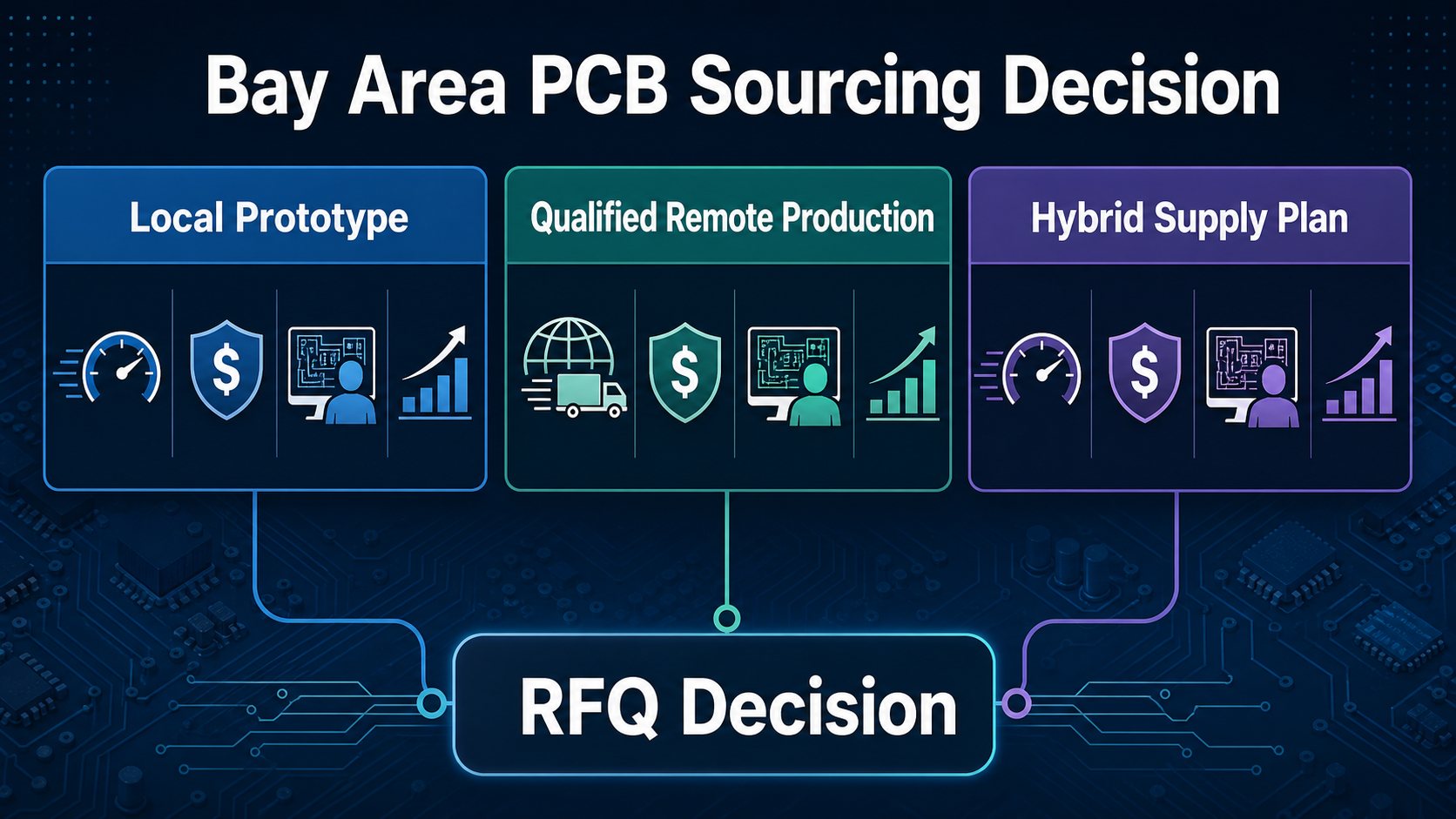
Choose local, remote, or hybrid supply according to where uncertainty remains in the project. Local prototyping is strongest when face-to-face access or a same-region handoff removes a real iteration bottleneck. Remote production becomes attractive when specifications are released and the project needs broader fabrication, PCBA, sourcing, or repeat-order support. A hybrid model can keep urgent prototypes close while qualifying a production path in parallel.

The image below is a decision aid, not a claim that one model is always better. Focus on the stage that carries the highest schedule or quality risk in your program.

Bay Area PCB sourcing decision comparing local prototype qualified remote production and hybrid supply plans
Local, remote, and hybrid PCB sourcing models solve different project constraints; the RFQ should expose which constraint matters most.
Supply Model Best Fit Main Risk Control
Local prototype Daily design changes, lab handoff, mechanical fit work Prototype decisions never become production documentation Freeze released files and record every approved deviation
Qualified remote production Stable design, repeat volume, integrated PCB + PCBA scope Longer communication loop when inputs are incomplete Complete RFQ, named owner, written response times
Hybrid supply Urgent learning plus planned transfer to repeat builds Two suppliers interpret files differently One controlled data package and a formal delta review

After choosing a model, define the exit condition. For example, a local prototype phase may end only after electrical validation, mechanical fit, BOM approval, and a released manufacturing data set are complete. That prevents an experimental build from becoming the undocumented master for production.

Compare Engineering Response Before Comparing Location

A supplier’s engineering response is measurable before an order is placed. Send the same controlled RFQ package and compare the questions returned. A useful response identifies contradictions, missing tolerances, ambiguous drill treatment, stackup assumptions, assembly-clearance risks, and acceptance gaps. A weak response simply says the files are manufacturable or gives a price without listing assumptions.

Set a small evaluation scorecard: time to acknowledge the package, time to return material questions, clarity of the DFM log, ownership of open items, and whether changes are tied to revision names. The goal is not the fastest email. The goal is the fastest closed decision with no hidden interpretation left on the production floor.

For a deeper review of fabrication rules, use the PCB design for manufacturability checklist as a companion to your supplier scorecard.

Buyer check: issue one deliberate ambiguity—such as an unspecified controlled-impedance stackup or a BOM/CPL mismatch—and observe whether the supplier catches it before quoting. Do not create a safety-critical trap; use a normal engineering question that should be found during review.

Separate Bare PCB, PCBA, Sourcing, and Testing Scope

Every Bay Area PCB quote should identify four independent scopes: fabrication, assembly, component sourcing, and verification. Without that split, a low number may only represent bare boards while another supplier has included stencil, setup, components, assembly, AOI, functional test, and packaging.

Scope Inputs Quote Must State
Bare PCB Gerber/ODB++, drill, drawing, stackup, fab notes Material assumptions, finish, tooling, electrical test, quantity
PCBA BOM, CPL, assembly drawing, polarity notes SMT/THT scope, stencil/setup, process, rework allowance
Component sourcing Manufacturer part numbers, alternates, approved vendors Pricing basis, availability date, substitution approval, excess material
Inspection and test Acceptance criteria, test method, fixtures, firmware Included records, fixture/NRE cost, failure disposition

When the project needs assembly, review EBest Circuit’s prototype PCB assembly service and component sourcing workflow as separate scope references. The RFQ should still state exactly which services apply to the current build.

Normalize Bay Area PCB Quotes by Total Landed Cost

Total landed cost is the amount required to receive acceptable hardware, not the unit price printed at the top of a quote. Normalize tooling, NRE, fabrication, components, assembly, inspection, test, packaging, freight, duties when applicable, payment cost, and expected engineering effort. Then compare the same quantity and delivery assumption.

Also separate one-time cost from recurring cost. A higher NRE line can be reasonable when it creates a reusable test fixture or controlled production setup. A low unit price can be misleading when repeated setup, unplanned component buys, or manual rework appears on every order. Record what happens to excess components, panels, stencils, fixtures, and engineering data after the build.

A simple normalized calculation is:

Total build cost = one-time engineering and tooling + recurring fabrication and assembly + components + verification + logistics + expected change/rework exposure.

Buyer check: ask each supplier to price the base case and one change case, such as a quantity increase or approved component alternate. The response shows whether the cost model can support the next project stage.

Plan Prototype Speed Without Sacrificing Production Transfer

A fast prototype is valuable only if the lessons from that build are captured in the released production package. Keep experimental changes out of email-only threads. If a pad is modified, a component is substituted, a stackup changes, or an assembly instruction is clarified, update the governing file and revision record.

Before the prototype starts, define what it must prove: electrical function, mechanical fit, thermal behavior, firmware interaction, assembly process, test coverage, or supplier process capability. After the build, close each result as pass, fail, or open action. That turns the prototype into evidence rather than a one-off board that happens to work.

For the transfer review, compare the prototype package against the intended production package line by line: fabrication drawing, stackup, Gerber/ODB++, drill, BOM, CPL, assembly drawing, approved alternates, firmware, test procedure, and packaging requirement. Any difference must have an owner and an approval status.

Check Material, Stackup, and DFM Assumptions Early

Material and stackup assumptions should be closed before price and lead time are treated as firm. Send the functional requirement, not only a material trade name. State controlled impedance, copper expectations, board thickness, surface finish, via structure, thermal constraints, and any drawing tolerances that affect fabrication.

For common rigid builds, EBest Circuit’s FR-4 PCB overview can help frame the product category, but the actual laminate family and stackup still require project confirmation. Do not infer a material, tolerance, or process limit from a general web page when the released drawing or supplier confirmation should govern the order.

Item Why It Changes the Quote RFQ Note
Stackup Controls layer construction, thickness, impedance, and material availability Provide target or allow supplier proposal with approval
Copper Affects trace geometry, etching, plating, thermal/current behavior State finished copper requirement where applicable
Via and hole rules Drive drilling, plating, fill/cap, and inspection needs Separate plated, non-plated, blind/buried, and filled features
Surface finish Changes process, shelf-life considerations, assembly interface, and cost State finish and any application-driven constraint

Buyer check: the supplier should return a proposed stackup or a clear confirmation—not silently price a default construction.

Control BOM, CPL, and Component Substitution Risk

Component risk is controlled by part identity, placement data, and an explicit substitution process. Each BOM line should have a manufacturer part number, description, quantity, reference designators, and approved-alternate status. The CPL must match the same board revision, coordinate origin, side, rotation convention, and designators used by the assembly drawing.

Ask who may propose an alternate, what evidence accompanies the proposal, and who approves it. A distributor listing or footprint match is not enough. Electrical rating, package, lifecycle, temperature, compliance, firmware interaction, and test coverage may all matter. Keep ā€œno substitution without written approvalā€ for controlled parts, but avoid making every commodity line a manual bottleneck if engineering has already defined acceptable alternates.

Observable result: before material purchase, procurement should be able to identify every not-found, long-lead, allocation, minimum-order, or alternate-request line in one exception list. If these issues remain hidden inside email threads, schedule confidence is low.

Define Inspection and Test Evidence Before the Build

Inspection and test should be selected from the failure risk and acceptance decision, not added as generic quality words. Bare PCB electrical test checks connectivity against supplied data. Visual and dimensional inspection address workmanship and drawing requirements. For PCBA, AOI can inspect visible placement and solder features; X-ray can support review of hidden joints; functional test verifies behavior under a defined setup. None of those methods replaces the others in every application.

Write what constitutes a pass, who supplies fixtures or firmware, what record is returned, how failed units are handled, and whether retest is permitted. The AOI in PCB manufacturing guide explains where optical inspection fits and why it cannot close hidden-joint or functional questions alone.

A useful acceptance plan lets the buyer observe a concrete result: quantity tested, method used, revision tested, pass/fail count, exception disposition, and record identifier. ā€œ100% testedā€ without a test definition is not an auditable promise.

Audit Traceability, Changes, and Repeat-Order Control

Repeatability depends on knowing exactly what was built, approved, inspected, and changed. Give every fabrication, assembly, and test package a revision. Maintain a question log with the requester, answer, approver, date, affected file, and disposition. When an exception changes the product definition, update the governing document rather than allowing the email to become the only record.

For repeat orders, ask the supplier to confirm the prior approved revision, open deviations, material or component changes, tooling status, and any process change that needs review. Buyers should be able to compare the new order release against the previous accepted build without reconstructing decisions from inbox history.

Observable result: pick one shipped board or assembly and trace it back to the fabrication files, BOM/CPL, approved questions, inspection/test record, and shipment. If the chain cannot be reconstructed, the repeat-order process needs stronger controls.

Prepare a Bay Area PCB RFQ Package Suppliers Can Price

A complete RFQ reduces price padding, engineering delay, and false quote comparisons. Put the following items in one controlled package and include a short scope sheet that names the requested services.

  1. Fabrication data: Gerber or ODB++, drill files, board drawing, stackup, impedance notes, panel preference if relevant, and revision identifier.
  2. Assembly data: BOM, CPL/centroid, assembly drawing, polarity notes, approved alternates, do-not-fit instructions, and revision identifier.
  3. Commercial data: prototype and forecast quantities, requested delivery point, schedule target, split-shipment needs, and quote validity expectation.

  4. Verification data: workmanship/acceptance requirements, inspection methods, electrical or functional test plan, fixtures, firmware, reports, and failure disposition.
  5. Change rules: who may answer engineering questions, who approves substitutions, how deviations are recorded, and which files govern after approval.

Ask suppliers to return an assumption-and-exclusion sheet with the quote. That sheet should identify proposed material, stackup status, unresolved DFM questions, sourcing exceptions, tooling/NRE, test scope, freight basis, and any item priced provisionally.

Buyer check: a colleague who was not in the original meetings should be able to read the package and understand what is being bought, how it will be accepted, and which decisions remain open.

Choose the Supply Model That Fits Your Project

Use a local supplier when proximity closes a specific engineering loop; use a qualified remote supplier when integrated scope, repeatability, or production economics matter more; use a hybrid model when both needs are real. The correct choice can change as the project matures.

  • Choose local-first when same-region physical access materially shortens prototype learning or failure analysis.
  • Choose remote-production-first when the package is stable and the program benefits from integrated fabrication, PCBA, sourcing, testing, or repeat builds.
  • Choose hybrid when an urgent prototype path and a scalable production path must be qualified at the same time.

EBest Circuit is not presented as a Bay Area local manufacturer. It is a direct RFQ comparison option for Bay Area buyers who want PCB fabrication, PCBA, DFM, BOM/CPL review, sourcing, inspection, and production planning evaluated together. Add that comparison early enough to expose scope and cost differences before the team is committed to a single path.

PCB Manufacturing Bay Area FAQ

Is a Bay Area PCB manufacturer always faster?
A local supplier may shorten physical handoffs and in-person engineering loops, but total lead time also includes DFM questions, material availability, component sourcing, test setup, approval, fabrication, assembly, and shipment. Compare the complete critical path.

What files are needed for a PCB manufacturing quote?
For bare boards, send Gerber or ODB++, drill files, drawing, stackup or stackup requirements, fabrication notes, quantity, and delivery target. Add BOM, CPL, assembly drawing, approved alternates, test requirements, and firmware or fixtures for PCBA.

Should a startup use a local prototype shop and another production supplier?
It can work well when the data package is controlled. Freeze the released files, document prototype deviations, and make the production supplier review the final package before volume commitments.

How do I compare a local PCB quote with an overseas quote?
Normalize fabrication, tooling, components, assembly, inspection, test, packaging, freight, duties when applicable, payment cost, and engineering effort. Also compare what happens after a design change or failed acceptance test.

What is a hybrid PCB supply plan?
A hybrid plan uses different suppliers or locations for different stages, such as local prototypes and qualified remote repeat production. It needs one controlled revision set and a formal transfer review to prevent interpretation gaps.

How can I test a supplier’s engineering response before ordering?
Send a controlled RFQ package and compare the quality of returned questions, assumption logs, response ownership, and revision references. A useful review should close ambiguities, not merely confirm that files can be opened.

What should a PCB quote list separately?
Ask for bare PCB, tooling/NRE, components, PCBA setup and assembly, inspection, test, packaging, freight, and applicable one-time charges as separate lines, together with assumptions and exclusions.

How should component substitutions be approved?
Require a documented proposal with manufacturer part number, reason, electrical and mechanical comparison, availability, price effect, and any test impact. Controlled parts should not change without written approval from the designated owner.

Which test records should a PCB or PCBA supplier return?
The answer depends on risk and scope. Define the method, revision, quantity tested, acceptance criteria, pass/fail result, exception disposition, and record identifier before the build.

Can EBest Circuit support Bay Area PCB buyers?
Yes. EBest Circuit can serve Bay Area buyers as a non-local RFQ comparison option for PCB fabrication, PCBA, DFM review, BOM/CPL review, component sourcing, inspection, testing coordination, and production planning, subject to project review and confirmation.

Before you commit to a Bay Area PCB supplier, compare the complete manufacturing path.

Send your Gerber or ODB++ files, drill data, drawings, stackup notes, BOM/CPL, quantity, material and surface-finish requirements, inspection/test plan, and target delivery date to sales@bestpcbs.com. EBest Circuit will review the PCB fabrication and PCBA scope, DFM questions, sourcing exceptions, acceptance evidence, and quote assumptions so your team can compare local, remote, and hybrid options with fewer hidden costs and fewer production surprises.

Send Files for a PCB Quote | Request an Engineering Review

You may also like