EBest Circuit (Best Technology) Co.,Ltd
- +86-755-2909-1601
- sales@bestpcbs.com

|
The ceramic PCB is widely applied to various industries, such as automotive electronics, communications, aerospace and so on. It possesses the characteristics of high temperature resistance and high insulation performance. The thick film technology can improve the insulation performance and resistance accuracy of the circuit. Meanwhile, it also reduce the influence of external temperature and humidity. Therefore, the thick film circuit has stronger external environment adaptability than independent soldering circuit. Since the thick film ceramic PCB possesses many benefits, then how to make it? Here are some steps about the fabrication of thick film ceramic PCB. |
|
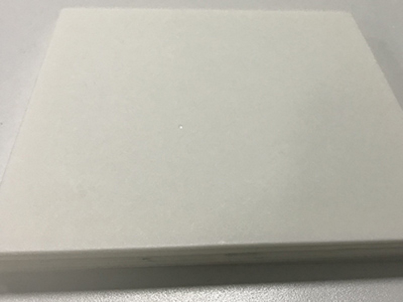
1、Raw materialThe size of the common ceramic substrate is 114*114mm. The specifications need to check the manufacturing capability of EBest Circuit (Best Technology). The picture below is the raw material before cutting: >Click For More |
 |
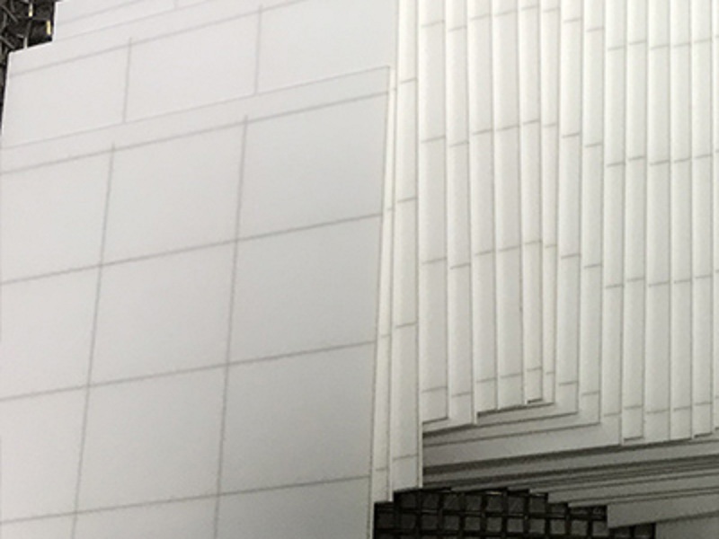
2、Substrate drilling and outline cuttingNow both the drilling technology and the outline cutting are using laser machine. But the laser energy is different, such as cold light source (UV light), carbon dioxide (CO2), fiber cutting and so on, >Click For More |
 |
3、Blackening spot removing after laser drillingAfter drilling, the protective material on the surface should be removed so that it can go to next step of copper spurring or conductive film printing, also the residue in the holes should be cleaned completely. >Click For More |
 |
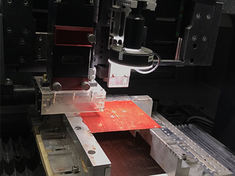
4、Make stencil for the trace according to the circuit drawingIn fact, the process of laser drilling/scribing and stencil making can be done at the same time, as they’re belonging to different production workshop. >Click For More |
 |
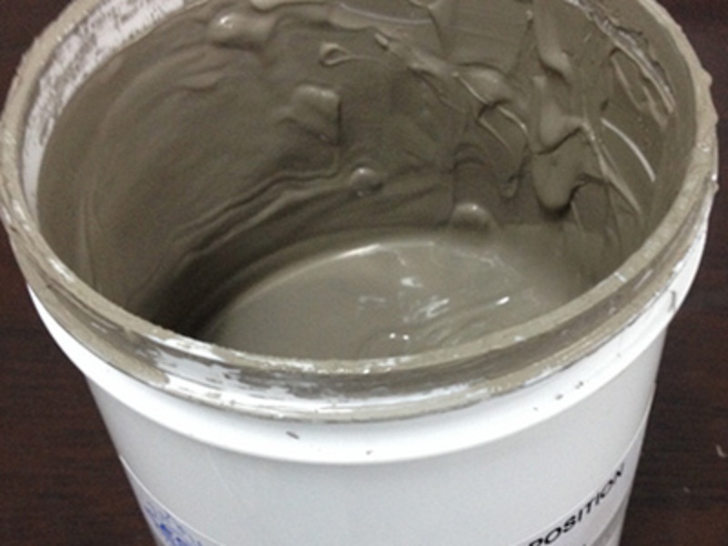
5、Conductive ink preparationDifferent conductive ink has different storage temperature. Base on the different storage temperature a certain thawing and warming time are needed. >Click For More |
 |
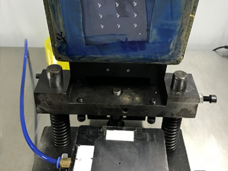
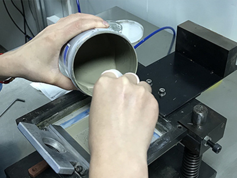
6.Sample makingAt sample making, it can be followed the procedures like this: Fixing the ceramic substrate on the base, Align the locations of the stencil and the substrate, Putting the ink on the stencil, >Click For More |
 |
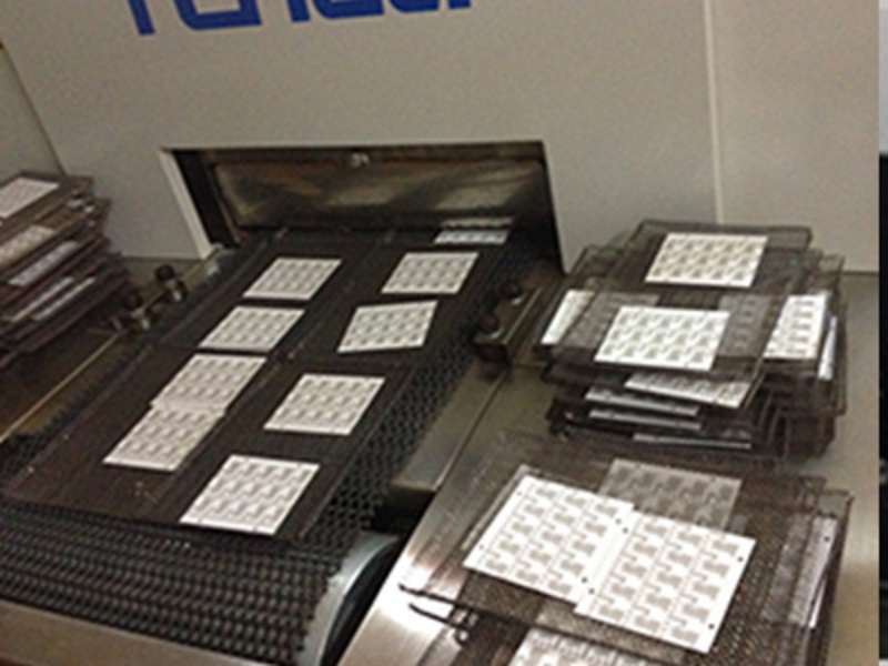
7、Spreading, drying and over the firing oven , so that ink can be combined with ceramic substrate.The detail steps after printing as below. If you still have questions about the Sample making, please click here to read more: 6.Sample making >Click For More |
 |
8、Printing resistance ink and laser resistor trimmingThe resistance ink can be printed after the conductor circuit was made. According to the different resistivity, only use the same value ink will be printed at a time. >Click For More |
 |
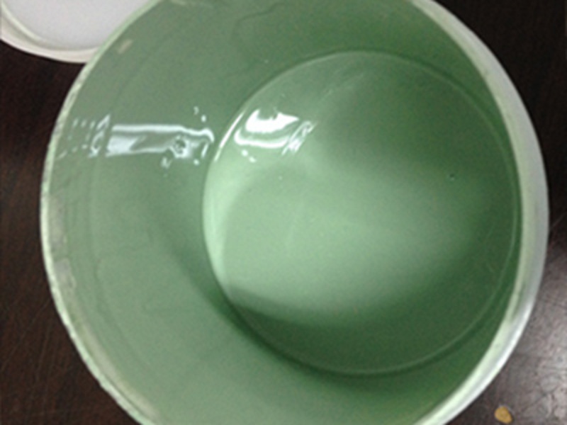
9、Printing glass glaze to protect the circuitBecause the manufacturing process is the same as printing conductive ink, here the details will not be shown again. The process is also printing, drying, high-temperature firing, >Click For More |
 |
10、Finished product testing, packing and shipment |
|
|
As a professional manufacturer of Ceramic PCB in China, EBest Circuit (Best Technology) is controlling each manufacturing process of thick film ceramic PCB, to make sure each piece of ceramic board is high quality in every step, and customers always receive ceramic board exactly according to their drawings. Welcome to contact us today for any enquiry for Ceramic PCB. |
|