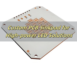
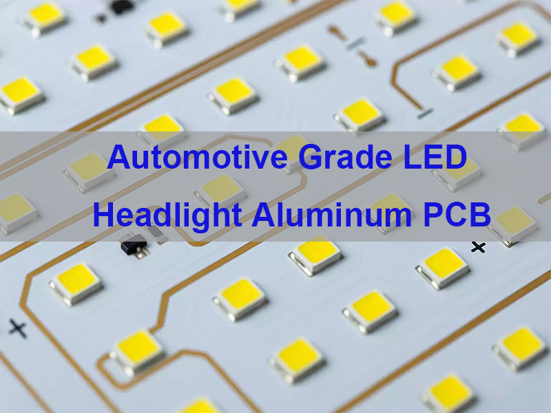
Automotive Grade LED Headlight Aluminum PCB is a specialized Metal Core Printed Circuit Board designed to provide superior heat dissipation for the high-power LEDs used in modern vehicle headlights, ensuring longevity, consistent light output, and safe driving. This blog will explore its critical role, advantages over standard boards, key design rules, materials, application scenarios, and how to select a reliable manufacturer.
Designing reliable automotive lighting is fraught with challenges. Many engineers face these common hurdles:
- Premature LED Failure: Inadequate heat sinking causes LEDs to overheat, leading to accelerated lumen depreciation and early burnout.
- Thermal Runaway and Safety Risks: Poor thermal management can cause unstable junction temperatures, risking thermal runaway which compromises both light performance and vehicle safety.
- Complex Thermal Management Design: Integrating effective heat dissipation into a compact, aesthetically pleasing headlight housing adds significant design complexity and cost.
- Difficulty Finding a Qualified Supplier: Sourcing a manufacturer with proven expertise in both high-thermal PCBs and stringent automotive-grade certifications (like IATF 16949) is a major bottleneck.
- Inconsistent Production Quality: Inconsistent manufacturing processes lead to variability in thermal interface performance (like dielectric layer quality), affecting the final product’s reliability.
Thankfully, partnering with a specialized PCB manufacturer can directly address these challenges. Here’s how a professional turnkey partner like us provides solutions:
- Superior Heat Dissipation Design: We specialize in Aluminum PCBs and SinkPad PCBs, which feature direct thermal paths to transfer heat away from LEDs efficiently, drastically reducing junction temperatures.
- Robust and Reliable Construction: Our PCBs are built with automotive-grade materials and processes that withstand high temperatures, thermal cycling, and vibrations, preventing thermal runaway.
- Expert DFM and Thermal Simulation Support: Our engineering team provides Design for Manufacturing (DFM) analysis and thermal guidance to simplify your design process, optimizing the layout for both performance and manufacturability.
- IATF 16949 Certified Automotive Manufacturing: As an IATF 16949:2016 certified facility, we have the quality management system specifically required for automotive components, ensuring process control and traceability.
- Strict Process Control and Quality Guarantee: We perform rigorous quality control at every stage, from raw material inspection (using equipment like X-Ray copper thickness testers) to final testing, guaranteeing consistent, high-quality output for every order.
At EBest Circuit (Best Technology), we are a professional PCB and PCBA manufacturer with 20 years of experience, specializing in high-performance boards like Aluminum PCBs and SinkPad PCBs. As a one-stop, full turnkey solution provider, we are equipped with the advanced manufacturing capabilities, strict quality certifications (including ISO 9001, IATF 16949, and RoHS), and engineering expertise to deliver reliable, automotive-grade solutions. We are your trusted partner for transforming demanding thermal management challenges into reliable, high-performance lighting systems. For your next project, pls feel free to contact us at sales@bestpcbs.com.
What Is Automotive Grade LED Headlight Aluminum PCB?
This section introduces the fundamental concept, composition, and primary function of the product.
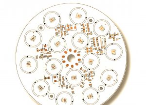
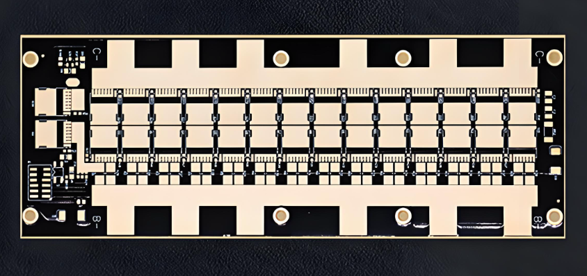
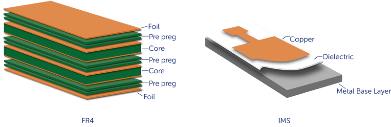
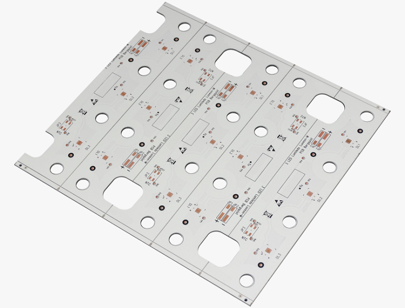
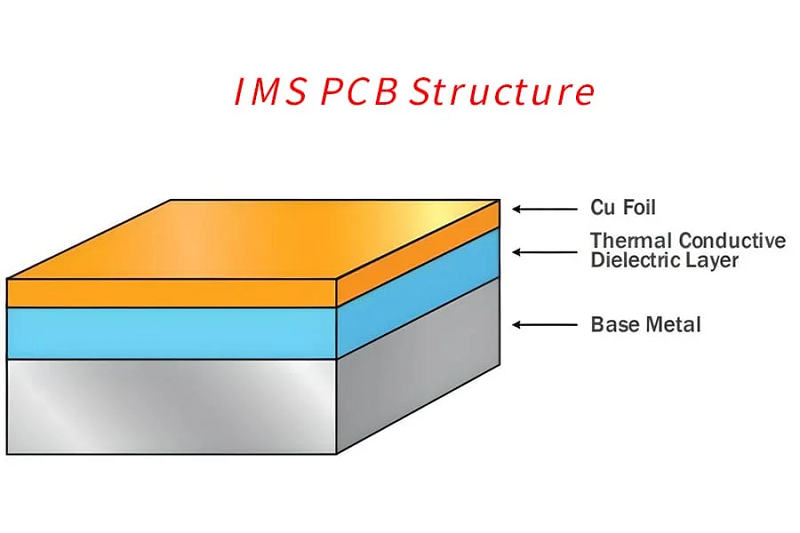
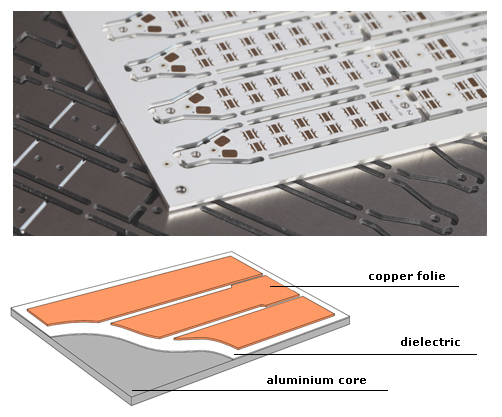
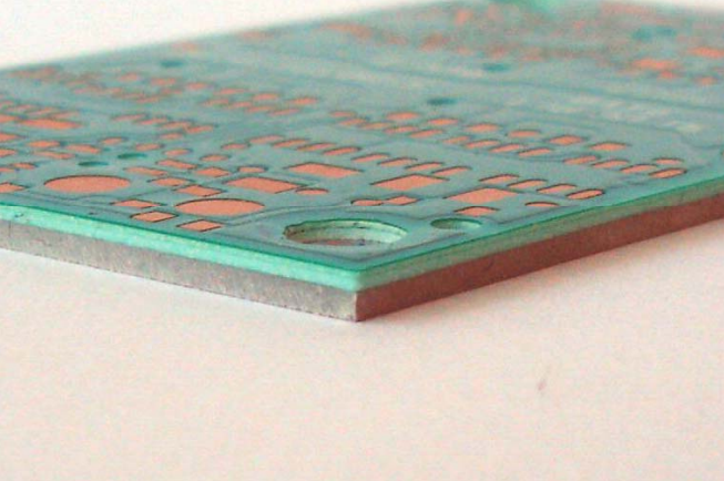
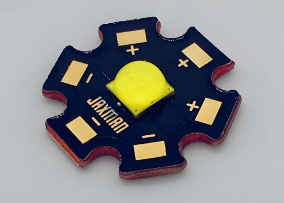
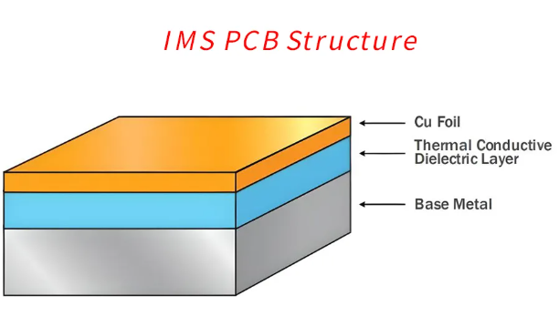
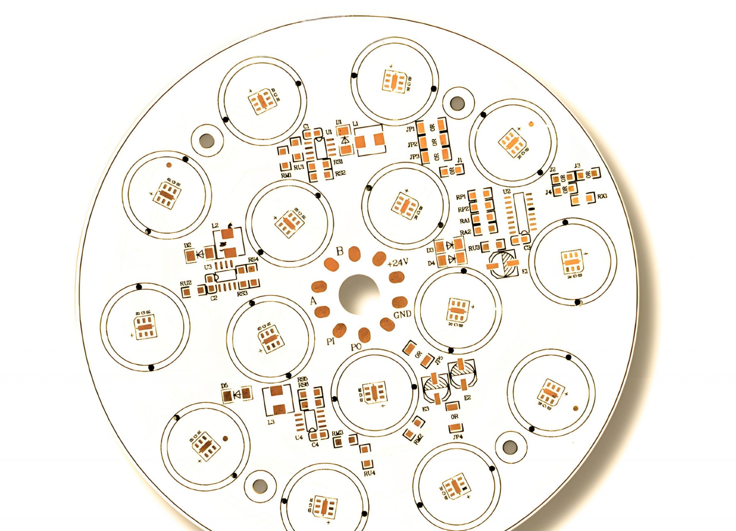
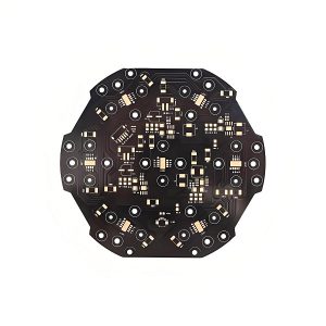
An Automotive Grade LED Headlight Aluminum PCB is a type of Metal Core PCB (MCPCB) specifically engineered to meet the rigorous reliability and performance standards of the automotive industry. Its core function is to serve as both the electrical interconnection platform and the primary thermal management solution for high-power LED arrays in headlights. The structure typically consists of a copper circuit layer, a thermally conductive but electrically insulating dielectric layer, and an aluminum base layer which acts as a heat spreader. This construction efficiently draws heat away from the LED chips, transferring it to a heat sink or the housing, which is critical for maintaining optimal LED performance, color consistency, and lifespan under the demanding conditions of an automotive environment.
Key characteristics include:
- High Thermal Conductivity: The dielectric layer is formulated for optimal heat transfer (e.g., 1.5W/m·K to 3.0W/m·K), far superior to standard FR4.
- Automotive-Grade Reliability: Materials and construction are selected to withstand extended temperature cycling, high humidity, and vibration, complying with standards like AEC-Q102.
- Robust Construction: Designed for mechanical stability and to facilitate efficient assembly (SMT) and thermal interface attachment.
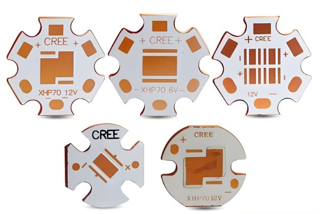
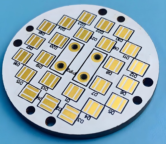
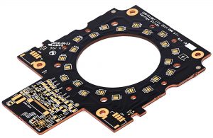
- Customizable Designs: Can be manufactured in various shapes, with different surface finishes (like ENIG or OSP for solderability), and with features like SinkPad technology for enhanced thermal performance.
In summary, it is the foundational component that ensures the thermal stability and long-term reliability of modern automotive LED lighting systems.
Why Choose Automotive Grade Aluminum PCB SinkPad For LED Headlight Over Standard MCPCB?
This section details the advanced benefits of the SinkPad design, directly comparing it to standard Aluminum PCBs.
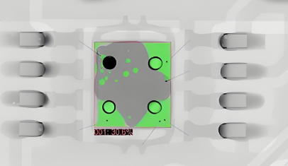
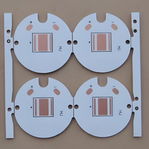
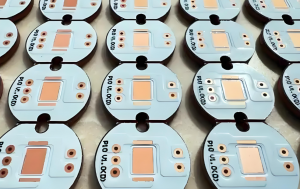
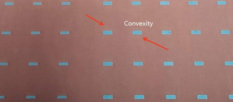
While standard Aluminum PCBs are excellent for heat dissipation, the Automotive Grade Aluminum PCB SinkPad represents a significant evolution, offering superior thermal and mechanical performance for the most demanding LED headlight applications. The key differentiator is the integration of a “SinkPad” – a thermally enhanced, often exposed metal pad or cavity within the board structure designed for direct thermal connection of the LED package. This minimizes the thermal path between the LED junction and the aluminum core.
Choosing a SinkPad Aluminum PCB for Automotive Grade LED Headlight provides these advantages:
- Lower Thermal Resistance: By eliminating layers (like solder mask and solder) between the LED and the metal core, SinkPad drastically reduces the junction-to-board thermal resistance (RθJ-B).
- Higher Power Handling: Enables the use of higher-power LED chips or allows for driving LEDs at higher currents without overheating, supporting brighter headlight designs.
- Improved Lumen Maintenance: Better temperature control at the LED junction directly translates to more stable light output and color over the product’s lifetime.
- Enhanced Mechanical Stability: The SinkPad structure can provide a more secure mounting platform for the LED, improving resistance to vibration—a critical factor in automotive applications.
- Design Flexibility: SinkPads can be customized in shape and depth to match specific LED packages, optimizing the thermal interface for various components on the same board.
Therefore, for cutting-edge, high-lumen automotive headlights where thermal performance is the limiting factor, a SinkPad Aluminum PCB is the superior choice over a standard MCPCB.
What Are The Key Layout Rules For LED Headlight Automotive Grade SinkPad Aluminum PCB?
This section provides practical design guidelines to maximize the performance and manufacturability of these specialized PCBs.
Effective layout is crucial to harness the full potential of an LED Headlight Automotive Grade SinkPad Aluminum PCB. Poor layout can create thermal hotspots, induce stress, and complicate manufacturing. Follow these key rules:
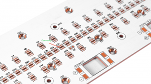
- Thermal Priority Placement: Cluster high-power LEDs evenly across the board to distribute the heat load. Avoid concentrating them in one area to prevent localized overheating.
- Optimize SinkPad Design: The SinkPad size and shape should precisely match the LED package’s thermal pad. Ensure adequate clearance (typically >0.5mm) between the SinkPad edge and surrounding copper traces to prevent short circuits.
- Trace Width and Current Capacity: Use wide, thick traces (copper weight of 2oz or higher is common) to carry the high current required by LEDs, minimizing resistive heating and voltage drop. Refer to IPC standards for current-carrying capacity.
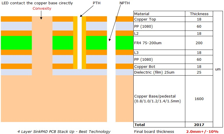
- Vias for Thermal Relief (if needed): For multilayer sections or to transfer heat to secondary layers, use an array of thermal vias filled with thermally conductive epoxy. However, in a pure SinkPad design, the goal is to minimize layers in the primary thermal path.
- Consider CTE Mismatch: The difference in the Coefficient of Thermal Expansion (CTE) between the LED package, solder, and PCB materials can cause stress during thermal cycling. Use a balanced layout and consider underfill for critical components.
- DFM for Automotive Environment: Adhere to stringent automotive DFM rules: sufficient creepage/clearance distances, robust solder mask dams, and avoidance of acute angles in traces to withstand vibration and contamination.
By adhering to these rules, designers can ensure their Automotive Grade LED Headlight SinkPad Aluminum PCB is both high-performing and reliably manufacturable.
What Materials And Stackups Are Used In Automotive Grade LED Headlight SinkPad Aluminum PCB?
This section breaks down the material composition and typical layer structures.
The performance of an Automotive Grade LED Headlight SinkPad PCB is directly dictated by its material selection and stackup. These materials are chosen for thermal conductivity, electrical insulation, reliability, and processability.
- Base Metal Core: Typically 5052, 6061, or 6063 aluminum alloy, with a thickness ranging from 0.8mm to 3.0mm, acting as the primary heat spreader.
- Dielectric Layer: A thin, polymer-based layer (e.g., epoxy filled with ceramic or boron nitride) with high thermal conductivity (0.8 to 3.0 W/m·K) and high dielectric strength (>3 KV/mm). This is the most critical material for performance.
- Copper Foil: Electro-deposited copper for the circuit layer, typically 1oz to 10oz in thickness, providing the conductive pathways.
- Surface Finish: Automotive-grade finishes like ENIG (Electroless Nickel Immersion Gold) or Immersion Silver are common for their excellent solderability, shelf life, and compatibility with automotive environmental testing.
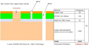
A typical Automotive Grade Aluminum PCB SinkPad for LED Headlight stackup is straightforward:
| Layer | Material | Main Role |
|---|---|---|
| Copper Layer | 2oz Copper + Solder Mask | Electrical connection and LED mounting |
| Dielectric Layer | Thermally Conductive Insulation | Isolation and heat transfer |
| Aluminum Base | 1.5mm Aluminum Alloy | Support and heat dissipation |
For more complex designs, a 2-layer Aluminum PCB might be used, incorporating a prepreg and a second copper layer, though this adds thermal resistance.
When Should You Use Automotive Grade LED Headlight SinkPad PCB In Automotive Lighting Design?
This section outlines the specific application scenarios that warrant the use of this advanced PCB technology.
Integrating an Automotive Grade LED Headlight SinkPad PCB is a strategic decision driven by thermal and performance requirements. You should consider it in the following automotive lighting design scenarios:
- High-Lumen / High-Power Headlights: When designing LED headlights with very high luminous output (e.g., matrix LED, laser high-beam modules) where the power density exceeds the cooling capacity of standard MCPCBs or FR4 boards.
- Compact Form Factors: In space-constrained designs (like sleek DRL/position light modules integrated into the headlight) where there is limited room for external heat sinks, requiring the PCB itself to be exceptionally efficient at heat spreading.
- Extended Lifespan & Warranty Requirements: For applications demanding ultra-high reliability and long lifespan (e.g., >30,000 hours) with minimal lumen depreciation, where controlling the LED junction temperature is paramount to meeting warranty goals.
- Hostile Thermal Environments: When LEDs are placed in locations with poor ambient airflow or high under-hood temperatures, a SinkPad PCB provides the necessary thermal headroom.
- Advanced Thermal Management Architectures: When the design uses a direct-attach method where the LED package’s thermal pad is soldered or bonded directly to the exposed metal of the SinkPad, eliminating thermal interface materials for the lowest possible thermal resistance.
In essence, this technology is the go-to solution when thermal performance is the critical bottleneck in achieving the desired brightness, size, reliability, and lifetime of the automotive lighting system.
How To Choose A Reliable Manufacturer For Automotive Grade LED Headlight SinkPad PCB?
This section provides a checklist for evaluating and selecting a suitable manufacturing partner.
Selecting the right partner is as crucial as the design itself. Here’s how to choose a reliable manufacturer for your Automotive Grade LED Headlight SinkPad Aluminum PCB:
- Proven Expertise in MCPCB/SinkPad: Look for a manufacturer with documented experience and case studies in producing Aluminum PCBs and specifically SinkPad designs. Review their capability charts for parameters like max layer count, thermal conductivity options, and dielectric strength.
- Automotive Quality Certifications: The manufacturer must hold IATF 16949:2016 certification. This is non-negotiable for automotive components. Additional certifications like ISO 9001 and ISO 14001 are strong indicators of a mature quality management system.
- Advanced Process and Equipment: Inquire about their dedicated process controls for SinkPad manufacturing (milling, plating, etching) and the equipment used (e.g., high-precision CNC routing machines, automatic optical inspectors, X-ray thickness testers). This ensures consistency and precision.
- Engineering Support (DFM/DFA): A reliable partner will offer proactive Design for Manufacturing/Assembly review, providing feedback on your design to improve yield, performance, and reliability. They should understand thermal and mechanical constraints.
- Supply Chain and Turnkey Capability: For PCBA projects, verify if they offer full turnkey services, including component sourcing from authorized distributors and in-house assembly with SMT capabilities for precision placement (e.g., handling 01005 components). This simplifies logistics and accountability.
- Transparent Communication and Samples: Assess their responsiveness and willingness to provide engineering samples or pre-production prototypes. Clear communication on lead times, supported by a track record of on-time delivery (e.g., 97% as noted in our profile), is essential.
Choosing a partner that excels in these areas will mitigate risk and ensure a smooth journey from design to mass production.
In conclusion, automotive Grade LED Headlight Aluminum PCB is the engineered thermal backbone that enables the reliable, high-performance operation of modern vehicle lighting, directly contributing to safer nighttime driving. This article has detailed its importance, the advanced benefits of the SinkPad design, critical layout and material considerations, ideal use cases, and a framework for selecting a qualified manufacturing partner.
For designers and engineers pushing the boundaries of automotive lighting, overcoming thermal challenges is paramount. EBest Circuit (Best Technology) stands as your ideal partner in this endeavor. With two decades of expertise in advanced PCB manufacturing, including specialized Aluminum PCBs and SinkPad PCBs, and a firm commitment to automotive-grade quality (IATF 16949 certified), we provide the reliable, high-performance solutions you need. From initial design support to full turnkey production, we are equipped to bring your most demanding Automotive Grade LED Headlight SinkPad Aluminum PCB projects to life with confidence. A warm welcome to start a conversation about your next MCPCB project by contacting us at sales@bestpcbs.com.
FAQs About Automotive Grade LED Headlight Aluminum PCB
This section addresses common, concise questions.
Q1: What is the main advantage of Aluminum PCB in LED headlights?
A1: Its primary advantage is superior heat dissipation. The aluminum base acts as a built-in heat spreader, drawing heat away from the LEDs to prevent overheating, which maintains brightness, color stability, and extends lifespan—critical for safe automotive lighting.
Q2: What is the difference between SinkPad and standard Aluminum PCB?
A2: A SinkPad PCB features a specially designed exposed thermal pad (the SinkPad) that allows the LED package to make direct thermal contact with the metal core, minimizing interfacial layers. A standard Aluminum PCB has a continuous dielectric layer and solder mask over the entire surface, resulting in a slightly higher thermal resistance between the LED and the core.
Q3: What certifications are vital for automotive-grade PCBs?
A3: IATF 16949:2016 is the core quality management system standard for the automotive industry. Material-level compliance with RoHS, REACH, and UL standards is also typically required.
Q4: What is the typical thermal conductivity of the dielectric layer?
A4: It varies. Standard dielectrics offer 0.8-1.5 W/m·K, while high-performance versions for demanding applications can reach 2.0 or 3.0 W/m·K. The choice depends on the power density and thermal design goals of the headlight.
Q5: Can you do PCBA assembly on these Aluminum PCBs?
A5: Yes, absolutely. As a full turnkey manufacturer, we provide complete PCB fabrication, component sourcing, and assembly (SMT and through-hole) services. Our SMT lines are equipped to handle assembly on Aluminum PCB SinkPad for Automotive Grade LED Headlight, including precise solder paste printing and reflow profiling for boards with high thermal mass.