PCB manufacturing PCB manufacturing
Home > Blog

PCB prototyping

Custom 5G IoT PCB Manufacturer in China with Turnkey Solutions
Friday, September 4th, 2026

EBest Circuit is a custom 5G IoT PCB manufacturer in China offering PCB fabrication, component sourcing, assembly, programming and testing. From early prototypes to repeat production orders, you can purchase bare boards or combine the work in a turnkey order.

We support boards for industrial gateways, routers, edge devices and remote monitoring equipment. Whether you supply the 5G modules or ask us to source the complete BOM, we coordinate the board build and assembly around your design, quantities and delivery requirements.

Send your Gerber files and BOM for a free DFM review. We can check manufacturing details, identify sourcing questions and prepare a quotation for the services you need.
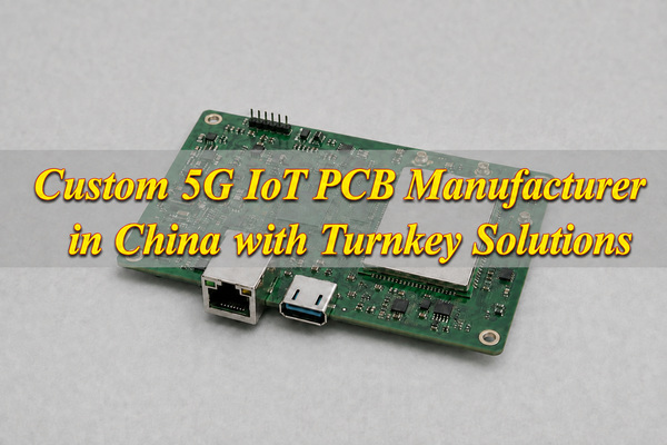
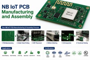
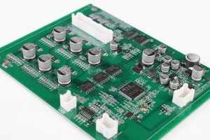
5g iot pcb manufacturer, conceptual unbranded gateway PCB assembly with a shielded module and edge connectors

What 5G IoT PCB Manufacturing and Assembly Services Do We Provide?

Our 5G IoT PCB manufacturing services cover bare boards, populated PCBs and box assembly. Choose the stages you need us to handle; you can retain your existing design or sourcing arrangements.

  • Custom PCB fabrication: Multilayer and HDI manufacturing support the routing and via requirements of compact boards. Provide the stackup, material, copper, finish and impedance specifications so we can review the complete construction.
  • Prototype and production builds: Start with samples for fit and functional evaluation, then order the accepted revision for small-batch or mass production. Changes found during testing should be incorporated before the next batch.
  • SMT and through-hole assembly: Assembly can combine dense IC packages and compact passives with through-hole connectors. Package pitch, board layout and joint access determine the soldering and inspection requirements.
  • Component sourcing: Full turnkey procurement covers the BOM; partial turnkey lets you supply selected modules or other parts. Exact part numbers and approved alternatives keep purchasing aligned with your design.
  • Programming, functional testing and box assembly: Add these services when the order requires programmed boards or assembled units. Supply firmware, test limits, fixture requirements and enclosure drawings so the deliverables are defined before production.

What 5G IoT PCB Manufacturing Capabilities Can We Support?

Our PCB fabrication capabilities include multilayer boards, HDI features and controlled impedance. The values below are process limits; the combination of features in your board needs engineering confirmation.

Manufacturing feature Capability
Standard trace / space 4 / 4 mil
HDI trace / space 2 / 2 mil
Standard minimum hole diameter 0.20 mm
HDI minimum hole diameter 0.10 mm
Impedance tolerance above 50 Ω ±10%
Impedance tolerance at or below 50 Ω ±5 Ω

What 5G IoT Applications Can We Support?

Our services support several types of 5G-connected equipment. Each puts different demands on the board layout, component selection and assembly:

  • Industrial gateways and routers: Module integration, multiple interfaces and external connectors can combine dense routing with mechanical constraints. Include the enclosure and connector positions in the fabrication and assembly review.
  • Edge computing devices: Processor and memory routing, power delivery and heat dissipation influence the board construction. Identify critical interfaces and cooling arrangements so the stackup and assembly access can be reviewed together.
  • Remote monitoring and tracking equipment: Compact packaging, antenna placement and power requirements can constrain component layout. Supply the operating conditions and mechanical drawings with the board files.
  • Connected meters and control equipment: Communication circuits share the board with sensing, power or field connections. Define the required clearances, connections and functional checks; the product’s electrical requirements remain part of the acceptance plan.

Can We Support 5G IoT PCB Prototypes and Mass Production?

We support PCB prototyping, small-batch production and mass production. You can evaluate a small batch before committing to a larger order, then carry the approved design and test requirements into repeat builds.

  • Prototype assembly: Use the first boards to check connector fit, programming access and product operation. Record any layout, component or firmware changes so the next batch incorporates what your team learned.
  • Small-batch production: Build a limited batch from the revised files to assess assembly consistency and the test procedure. Repeated rework or test failures need investigation before you increase the order quantity.
  • Sample approval: Your team reviews the samples and test records, then confirms the PCB revision, BOM, permitted alternatives and acceptance criteria. This approval gives production a clear specification to follow.
  • Mass production: We manufacture against the approved files. Agree on lot identification and delivery records so your receiving team can check each shipment and trace a problem to the relevant batch.

For repeat orders, tell us about changes to components, firmware or test limits before manufacturing starts. Even when the PCB layout stays the same, those changes can affect assembly or testing.

Can We Provide Component Sourcing and Turnkey 5G IoT PCB Assembly?

We can combine fabrication, BOM procurement and assembly in a turnkey order. The purchasing arrangement determines which parts EBest sources and which parts your team supplies.

  • Full turnkey: EBest sources the specified components and coordinates the PCB build and assembly. Send the full BOM and approved alternatives so availability can be reviewed before a delivery date is confirmed.
  • Partial turnkey: Supply selected items, such as modules or processors you already hold, and have EBest source the balance. Confirm quantities, packaging and arrival dates for your parts to avoid holding up assembly.
  • Consigned components: Your team provides the parts for assembly. Include exact part numbers, quantities and handling requirements so incoming checks can match them to the approved BOM.

For long-lead or obsolete parts, flag the affected BOM lines at quotation. We can review availability and proposed alternatives, but a substitute needs your engineering approval. Check the critical parts before committing to the production quantity.

How Do We Control Quality During 5G IoT PCB Manufacturing?

Our assembly quality checks cover incoming components, soldering and agreed functional tests. The inspection method depends on the defect being checked and whether the joint or circuit is accessible.

  • Incorrect or damaged incoming parts: Check identification and condition against the BOM before assembly. Resolve discrepancies before components enter the build.
  • Solder paste defects: SPI checks paste deposits before reflow, when a printing problem can still be addressed before soldering the components.
  • Placement and accessible solder defects: AOI supports inspection after assembly. Hidden BGA joints require a suitable method such as X-ray rather than an exterior visual check alone.
  • Board opens, shorts and impedance requirements: Specify the required electrical checks and impedance records with the fabrication order so results can be associated with the correct construction.
  • Product operation: Functional testing uses the agreed firmware, connections, test procedure and pass/fail limits. Specify any radio or network test separately, including its equipment and operating conditions.

Define the reports and lot or unit identification you need with delivery. Keep the accepted PCB revision, BOM and firmware connected to those records so a receiving or field issue can be investigated against the correct build.

How Do We Review 5G IoT PCB Designs Before Production?

A missing drill detail can hold up fabrication; a BOM mismatch can leave an assembly line waiting for the correct part. Our free DFM review, together with assembly checks, helps resolve these questions while the files can still be changed.

  • Check that the PCB files describe a buildable board. We review trace and space dimensions, hole sizes, via connections, copper clearances and the proposed stackup. For impedance-controlled nets, the drawing needs to identify the target and tolerance. If a fabrication note conflicts with the Gerber or drill data, we ask you to resolve the discrepancy before production. The output is a confirmed construction and a record of the changes you approved.
  • Match the components to the layout and assembly instructions. The BOM, placement data and assembly drawing should agree on reference designators, part numbers, orientation and unpopulated positions. A module variant with a similar name may have a different footprint or connector arrangement. We flag mismatches and review component spacing, solder-joint access and handling requirements so your team can correct the files before parts are fitted.
  • Keep programming and test connections accessible. A test point is of little use if a shield, connector or enclosure blocks it after assembly. Identify the programming interface and measurements needed for acceptance, then check probe access and fixture connections. Where access is restricted, agree on a layout change or an earlier test step. This gives the assembly team a usable test sequence and makes fixture preparation part of the schedule.

Send the latest revision of each file together and identify any unresolved design changes. We return manufacturing questions for your approval; RF performance, antenna operation and product compliance still require the appropriate design validation.

How Long Does 5G IoT PCB Manufacturing and Assembly Take?

For an initial schedule, allow about 10–12 days for qualifying 4–8-layer standard FR4 prototypes and about one week for PCBA. These are separate manufacturing references; the complete turnkey schedule also depends on component availability, test preparation and shipping.

Standard FR4 prototype fabrication is approximately 10 days for 4 or 6 layers and 12 days for 8 layers. These figures apply to orders below 1 mÂČ meeting our standard FR4 specifications. HDI, special laminates and other nonstandard constructions need a separate schedule. Assembly timing is confirmed against the quantity and test scope, with the required boards and components available.

The main factors that can move your delivery date are:

  • Board construction: Layer count, via structure, material, finish and quantity affect fabrication. Identify special laminates and HDI requirements at quotation so availability and processing time can be checked before you commit to a date.
  • Parts availability: PCB fabrication and purchasing can overlap, but assembly needs a complete kit. A missing module or connector can delay the batch even when the bare boards are ready. Send exact part numbers and flag customer-supplied items early.
  • Testing and design changes: Programming files, fixtures and pass/fail limits must be ready for assembly. A late component substitution or revised test procedure can require another review before work continues.
  • Capacity and transport: Production loading, holidays, shipping and customs clearance affect arrival. Give us the date you need the boards at your site; WIP updates let you follow progress during manufacturing.

Case Analysis: From 5G IoT PCB Prototypes to Mass Production

Project background: In this hypothetical project, a hardware team needs 10 assembled prototypes for evaluation. After sample approval, it plans to begin mass production with an initial 100-board production order. Each board uses one customer-supplied 5G module and two specified interface connectors. EBest would fabricate the PCBs, source the remaining BOM and assemble the boards.

Requirements and challenges: The prototype batch therefore needs 10 modules and 20 interface connectors; the first production order needs another 100 modules and 200 connectors. These are fitted quantities, excluding assembly spares. Purchasing the production components before prototype approval risks committing parts to a design that may change. The team also needs programming access after assembly and a way to identify each tested board.

Our proposed solution: Check the board files and BOM first, then confirm the prototype kit and any spare-parts allowance. Assemble the 10 prototypes using one approved PCB, BOM and firmware revision. Record the programmed version and the agreed power-up and interface-test results against each board identifier. After customer evaluation, incorporate approved changes and confirm the components for the first 100-board production order before procurement and assembly proceed.

Output and acceptance: The requested prototype delivery consists of 10 assembled boards and 10 individual test records, plus the list of approved manufacturing changes. With one module and two connectors per board, the first production order has a fitted-parts requirement of 100 modules and 200 connectors. Mass production begins after sample approval and confirmation of the revised BOM. For subsequent orders, the approved PCB files, BOM, firmware and test procedure provide the manufacturing specification; any changes need approval before the next batch. Actual yield, test performance and delivery time would come from the completed build records.

Why Choose EBest as Your 5G IoT PCB Manufacturer?

Choose EBest when you want PCB fabrication, sourcing and assembly managed together. You can keep control of the design and critical parts while we coordinate the manufacturing work.

  • Less supplier coordination: A turnkey order brings the bare boards, purchased components and assembly under one contact. When a layout or part changes, you can resolve its effect on the complete order without forwarding separate instructions to several suppliers.
  • Quality checks matched to your board: Incoming inspection, SPI, AOI, X-ray and functional testing address different defects. We agree on the relevant coverage and records with you, helping your team inspect deliveries and investigate problems against the correct batch.
  • Delivery planning that includes the parts: We review material and component availability alongside fabrication and assembly. WIP updates help you follow the order and coordinate your own testing or product integration around manufacturing progress.
  • Engineering support before you commit to production: Free DFM review identifies manufacturing conflicts in the submitted files. Resolving them before fabrication helps avoid building boards that need an immediate revision.
  • Flexibility as quantities grow: Start with samples and continue to small-batch or mass production orders using the approved design. Full turnkey, partial turnkey and consigned-parts options let you choose how much procurement you retain at each stage.

What Files Are Required for a 5G IoT PCB Quote?

Send the files and specify whether you need bare boards or assembled units. Include prototype and production quantities, the destination and your required arrival date.

  • PCB fabrication: Gerber or ODB++ data, drill files, fabrication drawing, stackup and PCB specifications. Identify material, copper, finish and impedance requirements so the quotation matches the construction.
  • PCB assembly: BOM, pick-and-place data, assembly drawing and approved alternatives. Mark customer-supplied components and their availability so the sourcing split is clear.
  • Programming and testing: Firmware, test procedure, fixture requirements and acceptance criteria. Specify reports, lot identification and any enclosure work required with delivery.

Send your Gerber files, BOM, quantities, testing requirements and delivery date to sales@bestpcbs.com for a quotation and free DFM review.

FAQs About 5G IoT PCB Manufacturing

Q1: What happens if a BOM component is obsolete or unavailable?

A1: We can review availability and suggest alternatives. Your engineering team must approve a substitute before purchase, including any effect on fit, electrical operation, firmware or compliance requirements.

Q2: Can we change components after approving the prototype?

A2: Yes, but submit the updated BOM before the next order. Review the effect on layout, programming and test limits, and decide whether the change needs another sample build.

Q3: What should accompany a customer-supplied test fixture?

A3: Include connection instructions, compatible firmware, the test procedure and pass/fail limits. Confirm when the fixture will arrive so testing can begin when the assembled boards are ready.

Q4: Can EBest quote while some design files are still being revised?

A4: Send the available files and mark the open items. We can begin a preliminary review; the final price and schedule depend on the confirmed specifications, quantities, BOM and testing requirements.

Q5: How should we handle firmware changes between batches?

A5: Identify the firmware version and programming method for each order. If the new version changes product behaviour, update the test procedure and pass/fail limits before that batch is programmed.

You may also like

Top 15 Heavy Copper PCB Manufacturers in USA
Friday, September 4th, 2026

Heavy copper PCB manufacturers in USA range from specialists in very thick conductors to suppliers that fabricate, assemble, and test complete boards. Choosing between them requires matching copper distribution, holes, and the complete layer stack to a process available at the required US site.

A 20 oz outer-layer power board needs a different manufacturing process from a 4 oz prototype supplied with components assembled. Copper capability determines which suppliers can build the board; engineering support, assembly services, and the prototype-to-production route determine which can deliver the complete order.
Heavy copper PCB manufacturers in USA, editorial cover combining a heavy copper PCB product photograph with a US flag

Top 15 Heavy Copper PCB Manufacturers in USA Compared

Amitron and Pro-Tech offer specialized thick-copper processes, while Cirexx, PNC, Sierra, and Gorilla combine fabrication with assembly services. Larger networks such as FTG, Sanmina, and TTM offer multiple production locations, making the selected factory as important as the company’s overall capability.

Manufacturer Heavy Copper Capability Advantages Lead time Services
1. AmitronElk Grove Village, IL 20+ oz finished copper Mixed copper weights within one layer Quoted per heavy-copper order PCB fabrication
2. Pro-Tech Interconnect SolutionsChaska, MN Extreme copper: above 20 to 120 oz Local copper buildup for power paths and holes Quoted per heavy-copper order PCB fabrication; selective plating
3. AdvancedPCBMultiple US sites Up to 4 oz inner; 20 oz outer Mixed-weight layers with design support Quoted per heavy-copper order PCB design support; fabrication
4. Saturn ElectronicsRomulus, MI Up to 20 oz US double-sided and multilayer boards Quoted per heavy-copper order Bare PCB fabrication
5. Excello CircuitsAnaheim, CA 0.5–4 oz inner; 1–20 oz outer Prototype and repeat-build support Quoted per heavy-copper order Prototype and production PCB fabrication
6. Cirexx InternationalUS in-house PCB site Up to 4 oz inner; 6 oz outer Layout, PCB assembly and test Quoted per heavy-copper order PCB layout; fabrication; assembly; testing
7. PNC Inc.Nutley, NJ 0.5–8 oz published range Design and assembly at one US site Quoted per heavy-copper order PCB design; fabrication; assembly
8. Sierra CircuitsUS PCB sites Advanced: up to 6 oz inner and finished outer Advanced boards with assembly Quoted per heavy-copper order PCB fabrication; component sourcing; assembly
9. Gorilla CircuitsSan Jose, CA 4 oz stated maximum In-house PCB, assembly and test Quoted per heavy-copper order PCB fabrication; assembly; testing
10. Bay Area CircuitsSilicon Valley, CA Up to 4 oz inner; 5 oz outer, finished Local and offshore PCB options Quoted per heavy-copper order PCB fabrication; offshore sourcing
11. Omega Circuits & EngineeringNew Brunswick, NJ Up to 9 oz Metal-based boards and heat sinks Quoted per heavy-copper order PCB fabrication; assembly with customer-supplied parts
12. American Standard CircuitsWest Chicago, IL Heavy copper; confirm layer limits Heavy copper and thermal board options Quoted per heavy-copper order PCB fabrication; global sourcing
13. FTG CircuitsCA, VA, MA and MN Heavy copper; confirm site limits US sites with varied PCB processes Quoted per heavy-copper order PCB fabrication; new-product introduction
14. SanminaSan Jose, CA; other US sites Above 6 oz group offering; confirm US site US new-product builds and global supply Quoted per heavy-copper order PCB fabrication; new-product introduction
15. TTM TechnologiesMultiple US sites; global network 2–12 oz auto offering; confirm US site Auto power boards and multiple sites Quoted per heavy-copper order PCB fabrication
Manufacturer Heavy Copper Capability Advantages
1. AmitronElk Grove Village, IL 20+ oz finished copper Mixed copper weights within one layer
2. Pro-Tech Interconnect SolutionsChaska, MN Extreme copper: above 20 to 120 oz Local copper buildup for power paths and holes
3. AdvancedPCBMultiple US sites Up to 4 oz inner; 20 oz outer Mixed-weight layers with design support
4. Saturn ElectronicsRomulus, MI Up to 20 oz US double-sided and multilayer boards
5. Excello CircuitsAnaheim, CA 0.5–4 oz inner; 1–20 oz outer Prototype and repeat-build support
6. Cirexx InternationalUS in-house PCB site Up to 4 oz inner; 6 oz outer Layout, PCB assembly and test
7. PNC Inc.Nutley, NJ 0.5–8 oz published range Design and assembly at one US site
8. Sierra CircuitsUS PCB sites Advanced: up to 6 oz inner and finished outer Advanced boards with assembly
9. Gorilla CircuitsSan Jose, CA 4 oz stated maximum In-house PCB, assembly and test
10. Bay Area CircuitsSilicon Valley, CA Up to 4 oz inner; 5 oz outer, finished Local and offshore PCB options
11. Omega Circuits & EngineeringNew Brunswick, NJ Up to 9 oz Metal-based boards and heat sinks
12. American Standard CircuitsWest Chicago, IL Heavy copper; confirm layer limits Heavy copper and thermal board options
13. FTG CircuitsCA, VA, MA and MN Heavy copper; confirm site limits US sites with varied PCB processes
14. SanminaSan Jose, CA; other US sites Above 6 oz group offering; confirm US site US new-product builds and global supply
15. TTM TechnologiesMultiple US sites; global network 2–12 oz auto offering; confirm US site Auto power boards and multiple sites
Manufacturer Lead time Services
1. AmitronElk Grove Village, IL Quoted per heavy-copper order PCB fabrication
2. Pro-Tech Interconnect SolutionsChaska, MN Quoted per heavy-copper order PCB fabrication; selective plating
3. AdvancedPCBMultiple US sites Quoted per heavy-copper order PCB design support; fabrication
4. Saturn ElectronicsRomulus, MI Quoted per heavy-copper order Bare PCB fabrication
5. Excello CircuitsAnaheim, CA Quoted per heavy-copper order Prototype and production PCB fabrication
6. Cirexx InternationalUS in-house PCB site Quoted per heavy-copper order PCB layout; fabrication; assembly; testing
7. PNC Inc.Nutley, NJ Quoted per heavy-copper order PCB design; fabrication; assembly
8. Sierra CircuitsUS PCB sites Quoted per heavy-copper order PCB fabrication; component sourcing; assembly
9. Gorilla CircuitsSan Jose, CA Quoted per heavy-copper order PCB fabrication; assembly; testing
10. Bay Area CircuitsSilicon Valley, CA Quoted per heavy-copper order PCB fabrication; offshore sourcing
11. Omega Circuits & EngineeringNew Brunswick, NJ Quoted per heavy-copper order PCB fabrication; assembly with customer-supplied parts
12. American Standard CircuitsWest Chicago, IL Quoted per heavy-copper order PCB fabrication; global sourcing
13. FTG CircuitsCA, VA, MA and MN Quoted per heavy-copper order PCB fabrication; new-product introduction
14. SanminaSan Jose, CA; other US sites Quoted per heavy-copper order PCB fabrication; new-product introduction
15. TTM TechnologiesMultiple US sites; global network Quoted per heavy-copper order PCB fabrication

How Do You Choose a Heavy Copper PCB Manufacturer?

The right manufacturer must support the copper distribution and geometry in your drawing, then deliver the required bare board or assembly at the intended volume. A supplier’s maximum copper weight is only one part of that decision. Use the design and build requirements to make these five choices:

  • Match copper to the correct layers. List the required finished copper on every layer before screening suppliers. If a design needs 6 oz internally, a published 20 oz outer-layer capability with a 4 oz internal limit is not a suitable match. Request a custom-process review or select a supplier whose stated internal range covers the design.
  • Choose uniform, mixed-layer, or selective copper construction. Thick power traces and fine control routing may need different copper weights across layers or localized buildup within one layer. Show those regions on the drawing and ask whether the supplier’s etching, plating, and lamination process supports the transitions without widening the board or rerouting critical features.
  • Review current-carrying connections and heat removal. Send the terminal, hole, and heat-sink interface details with the copper specification. A thick trace still needs suitable connections and a path for dissipating heat. Choose a manufacturer that can review these features together and identify the geometry or assembly changes required before fabrication.
  • Decide whether to buy bare boards or a complete assembly. A fabrication specialist can suit a design with an established assembly partner. For a populated prototype, compare suppliers that can coordinate board fabrication, component supply, soldering, and the required tests; confirm which of those services are included in the quotation.
  • Match the supplier to the next production stage. Request prices and schedules for both the initial lot and expected repeat quantity. Identify changes in factory, material, or process between those stages. If domestic fabrication or a specific qualification is required, retain only suppliers able to meet it for both builds.

1. Amitron

Amitron’s main distinction is combining very thick conductors with lighter circuitry. The Illinois manufacturer publishes 20+ oz finished copper and a process called Laminated Deposition. It also describes multiple copper weights on the same layer, making it a candidate when a power path and its control circuitry need to share one board.

For a mixed-weight design, request the permitted transition geometry, conductor spacing, and solder-mask coverage at each copper height. Specify hole-wall copper separately: the surface-copper rating does not define the plating inside a current-carrying hole.

2. Pro-Tech Interconnect Solutions

Pro-Tech’s Chaska operation deserves consideration when copper must be concentrated in selected features. Its heavy and extreme copper offering extends above 20 oz to 120 oz for extreme constructions. Selective plating also allows localized buildup on conductors and plated-through holes, rather than requiring one copper height throughout the design.

Send a drawing of the thickened regions and their connections to lighter circuitry. Ask for achievable height, coplanarity, spacing, and hole-plating limits for that construction. The extreme-copper figure is not a blanket specification for every multilayer or selective feature.

3. AdvancedPCB

AdvancedPCB is an option for multilayers that combine thick external power conductors with lighter internal routing. Its custom capability table lists up to 4 oz inner copper and 20 oz outer copper, alongside mixed-weight stackups and design support. APCT, Advanced Circuits, and San Diego PCB Design now sit under this combined business.

Have the proposed factory approve copper weights, layer count, holes, and spacing together. A design requiring 20 oz on internal layers is not covered by the published 20 oz outer-layer figure; that distinction can eliminate an unsuitable quote before layout is finalized.

4. Saturn Electronics

Saturn is a Romulus, Michigan bare-board fabricator with double-sided and multilayer capability up to 20 oz. It is a direct candidate for domestic high-copper fabrication when component sourcing and assembly are being handled separately.

Check the required qualification against the actual copper construction. Saturn’s page distinguishes its stated UL scope of up to 6 oz on inner and outer layers from its fabrication capability up to 20 oz. Those are different claims; request current construction-specific documentation if qualification is required.

5. Excello Circuits

Excello’s Anaheim operation combines prototype and production fabrication with a clearly divided copper range: 0.5–4 oz internally and 1–20 oz externally. That makes it a candidate for thick outer-layer power boards expected to move from development batches to repeat orders.

Obtain a proposed production stackup with the prototype quote. Ask whether copper geometry, materials, and manufacturing site will remain the same at the intended volume, and have any production-driven design changes identified before approving the first build.

6. Cirexx International

Cirexx combines in-house US fabrication with layout, assembly, and testing. Its stated limits of 4 oz inner and 6 oz outer copper place it among the integrated options for a populated power board rather than a 20 oz bare-board requirement.

Define the assembly and test deliverables, including high-current terminals, programming, and functional checks where needed. Request review of soldering access and thermal demands around heavy-copper connections; fabrication acceptance alone does not settle the assembly process.

7. PNC Inc.

PNC brings design, fabrication, and assembly into its Nutley, New Jersey facility. Its published copper range is 0.5–8 oz. The single-site model is a useful distinction when fabrication and assembly questions need to be resolved together during power-board development.

Ask which inner- and outer-layer combinations the 8 oz figure covers. Use the approved layer-by-layer stackup as the basis for the combined fabrication and assembly quote.

8. Sierra Circuits

Sierra offers US PCB fabrication with component procurement and assembly options. Its current product comparison assigns up to 6 oz inner copper and 6 oz finished outer copper to the Advanced PCB service. A heavy-copper prototype therefore needs a quote for that service rather than the standard online product.

Request the advanced construction explicitly. The same comparison lists lighter copper for standard and bundled quick-turn products, so a general prototype price or advertised turnaround does not establish the price or schedule for a 6 oz assembled board.

9. Gorilla Circuits

Gorilla pairs PCB fabrication with assembly and test operations in San Jose. Its published FAQ states a maximum of 4 oz. It is a candidate for integrated 4 oz builds where the fabrication and assembly route is as important as the copper rating.

Establish whether repeat orders will use the in-house facilities or a fabrication partner; Gorilla also describes high-volume partner options. For a US-only order, have both the prototype and production quotes name the approved fabrication location.

10. Bay Area Circuits

Bay Area Circuits’ advanced matrix specifies finished copper up to 4 oz internally and 5 oz externally. Those limits refer to the completed conductor, including the finished-copper requirement used in the fabrication drawing. It offers both local fabrication and offshore sourcing.

Name the required manufacturing route in the RFQ and compare the resulting price and schedule on that basis. A local fabrication requirement should remain explicit when moving from a prototype order to a larger batch.

11. Omega Circuits & Engineering

Omega publishes American-built PCBs from New Brunswick, New Jersey and heavy-copper capability up to 9 oz. Metal-based boards and custom heat sinks broaden the discussion when the design needs a defined heat-removal path as well as substantial copper conductors. Assembly is also offered, generally with customer-supplied components.

Provide the mechanical thermal interface and identify whether heavy copper, a metal-based construction, or a separate heat sink is required. These portfolio options are not automatically combined in one board. For assembly, agree on component supply and responsibility for missing or unsuitable parts.

12. American Standard Circuits

American Standard Circuits manufactures in West Chicago and offers heavy copper within a portfolio that includes metal-backed, RF, flex, and rigid-flex technologies. It is worth evaluating when the board architecture is still being selected to balance electrical and thermal requirements.

Request a numerical copper limit and accepted geometry for the proposed stackup before including ASC in a copper-range comparison. Also distinguish West Chicago fabrication from the company’s global sourcing options before comparing its offer with a domestic-only quote.

13. FTG Circuits

FTG’s US locations include Chatsworth, Fredericksburg, Haverhill, and Minnetonka. Its group portfolio includes heavy copper, thermal management, RF, and rigid-flex technologies. The network is relevant when a program needs several specialized board types and a coordinated supplier relationship.

Route the heavy-copper drawing to a named facility and obtain that site’s copper and geometry limits. Group-level technology coverage does not mean every plant supports every construction, nor that separate RF, rigid-flex, and heavy-copper capabilities can be combined without a design review.

14. Sanmina

Sanmina combines domestic PCB fabrication and new-product introduction with an international production network. Its San Jose fabrication material includes heavy copper; its group technology material describes constructions above 6 oz. The sourcing question is how to carry an approved early build into the intended production route.

Identify the factory offering the required copper weight and the factory planned for repeat orders. If those differ, include transfer qualification, approved material substitutions, and pilot-build acceptance in the plan. The group-level above-6-oz figure alone does not establish a US plant’s limits.

15. TTM Technologies

TTM’s automotive portfolio lists 2–12 oz copper within a global network that includes multiple US fabrication sites. It is a candidate for automotive power programs where supplier qualification and continuing production support matter alongside the board technology.

Ask TTM to identify the plant supporting the specified automotive construction, then confirm whether it satisfies the US fabrication requirement. The portfolio’s 12 oz maximum is not evidence of 12 oz availability at every domestic site; approval should follow the selected plant and stackup.

Which Manufacturers Match Different Heavy Copper PCB Requirements?

Heavy-copper projects place different demands on a supplier: a very thick power conductor needs a suitable copper process, a populated prototype needs assembly coordination, and a heat-limited design needs a defined thermal interface. The supplier groups below connect those requirements to the capabilities described in the company profiles, with the layer or factory details that need confirmation.

  • Around 20 oz or heavier: compare Amitron, Saturn, AdvancedPCB, and Excello for their stated 20 oz-class offerings. AdvancedPCB and Excello specify that figure for outer layers. Pro-Tech is another candidate for extreme constructions beyond 20 oz; its process needs a separate geometry review.
  • Selective or mixed-weight copper: examine Pro-Tech for localized plating and Amitron for multiple weights on the same layer. AdvancedPCB describes mixed-weight multilayer stackups. Different weights across layers and different heights within a layer are separate construction requests.
  • A fabricated and assembled board: compare Cirexx, PNC, Sierra, and Gorilla within their copper ranges. Distinguish component procurement, assembly, and test in the quote; specify the included parts, assembly work, and tests as separate deliverables.
  • A defined heat-removal interface: include Omega and American Standard Circuits when evaluating metal-based or heat-sink-related alternatives alongside heavy copper. Select the structure against the actual thermal path, rather than assuming the thickest conductor solves every hot spot.
  • Multiple plants or a production transfer: examine FTG, Sanmina, and TTM at the facility level. A network can offer sourcing options, but the chosen copper construction and US production requirement must survive any proposed site change.

How Should You Compare Heavy Copper PCB Quotes?

Heavy-copper quotations can differ in finished copper, conductor spacing, hole plating, and test scope even when they use the same copper-weight label. Send each supplier the same drawing revision and request a written response against the technical requirements below. Once the construction is aligned, compare total lot price, tooling, included testing, assembly, freight, and delivery date at the same quantity.

Specification Equivalent quote requirement
Finished copper by layer The same completed conductor requirement and tolerance on each named layer. Starting foil weight and added plating must not be mistaken for interchangeable finished-copper specifications.
Geometry at that copper weight Accepted conductor width, spacing, pads, and copper-height transitions for the proposed process. A general fine-line minimum is not proof of the same spacing at maximum copper weight.
PTH and terminal connections Separate hole-wall plating and finished-hole requirements, including current-carrying terminal holes. Agree on how plating thickness will be verified; thick surface copper does not specify the barrel.
Complete layer stack The same layer count, copper distribution, dielectric construction, and finished thickness. Maximum layer count and maximum copper weight must be supported together, not taken independently from a capability table.
Reliability acceptance Agreed inspection and electrical-test records. Where thermal cycling is required, define samples, conditions, measurements, and pass/fail criteria; a general quality certificate does not supply these details.
Prototype and production route The approved factory, process, and change-control requirements for each build stage. Separate one-time qualification costs from recurring board cost so the volume comparison remains meaningful.
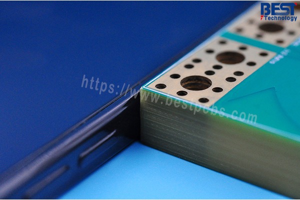
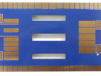
EBest Circuit heavy copper PCB product photograph showing the board edge and drilled openings

How Can You Verify US Heavy Copper PCB Fabrication?

A domestic-production requirement applies to the factory making the bare board, including any subcontracted work covered by that requirement. Suppliers with US sales, assembly, or multiple manufacturing sites may offer more than one production route. Establish the actual route before placing the order, then use quotation, process, and delivery records to verify it through these six checks:

  • Identify the actual fabrication site. Ask for the legal manufacturer and factory address on the quotation. Separate bare-board fabrication from sales, component sourcing, and assembly. If a broker or group sales team handles the order, obtain the producing site’s identity before approving it.
  • Confirm that site’s heavy-copper capability. Submit the proposed stackup and ask the factory to accept the required copper by layer, conductor spacing, hole-wall plating, and finished thickness together. A group capability page is insufficient when its thickest-copper process belongs to another location.
  • Clarify subcontracted processes. Ask which operations the selected site performs and whether plating, special finishes, testing, or other work goes to an outside provider. Obtain the proposed locations and responsibilities for the operations that affect your sourcing requirements.
  • Check the relevant records. Where the order requires a quality-system certificate or construction qualification, verify the named facility, scope, and current validity. Request sample inspection or test-report formats to establish the delivery evidence; agree which reports must accompany each delivered lot.
  • Separate prototype and production routes. Confirm the site, materials, and process planned for both stages. If volume orders may move to a partner or offshore factory, resolve that proposal before prototype approval and define the additional qualification needed for a transfer.
  • Bind the approved route to the order. Put the agreed fabrication location and change-approval requirements in the purchase documents. At delivery, match the lot identification, manufacturer records, and agreed inspection reports to that route. Investigate discrepancies before accepting a changed source.

Heavy Copper PCB RFQ Checklist

A heavy-copper RFQ needs enough information to price the board, review its manufacturability, and define the delivery scope. Fabrication files describe the layout, while operating conditions, test requirements, and build quantities identify work that may change the construction or quotation. Assemble the following information into one revision-controlled package:

  • Board and copper definition: Gerber or ODB++, drill files, fabrication drawing, stackup, material, and finished thickness. Specify finished copper and tolerance by layer; show selective buildup areas and any required starting foil separately. Mark a provisional stackup clearly and request written approval of proposed changes.
  • Current and temperature limits: identify high-current paths, continuous or pulsed load, duty cycle, allowable voltage drop, ambient conditions, and maximum permitted temperature rise. These inputs support review of the proposed conductor geometry; copper weight alone is not a current rating.
  • Critical geometry and connections: highlight minimum conductor width/spacing, copper-height transitions, high-current terminal pads, finished-hole sizes, and hole-wall plating requirements. Include connector or busbar interface drawings where relevant.
  • Acceptance and quantities: define electrical testing, inspection records, and any thermal-cycling or product-specific qualification requirements. State prototype, pilot, and production quantities, target dates, and the required fabrication country.
  • Assembly scope: include the BOM, placement data, assembly drawing, and component-sourcing responsibilities. Flag power terminals, heat sinks, programming, and functional-test requirements that must be included in the assembled-board quote.

How Can EBest Circuit Support Your Heavy Copper PCB Project?

EBest Circuit combines heavy copper PCB manufacturing, component sourcing, and PCB assembly for projects that permit manufacturing in China. Its services can help you resolve board requirements before ordering and coordinate fabrication with the parts and assembly work needed for delivery. The practical benefits are:

  • Identify manufacturing issues before committing to a build. A free DFM review gives you an opportunity to resolve copper spacing, holes, and construction questions before fabrication. Submit the stackup and design files early so proposed changes can be assessed before components and assembly plans depend on the board revision.
  • Translate the heavy-copper design into a clear fabrication requirement. Review finished copper by layer, critical connections, and any selective buildup with the board manufacturer. An agreed construction gives your engineering and purchasing teams a common basis for approving the quotation and checking whether a proposed change is acceptable.
  • Reduce handoffs between fabrication and assembly. PCB manufacturing and assembly services let you discuss the bare board, power terminals, heat sinks, and component placement within one order scope. This helps bring soldering and assembly-access requirements into the board review before the design is released.
  • Coordinate component purchasing with the assembly order. Component-sourcing support can reduce the separate purchasing work needed for a populated board. Provide the BOM, exact part numbers, and acceptable alternatives; confirm proposed substitutions and their effect on availability before approving procurement.
  • Plan prototype and repeat orders together. Discuss the initial quantity, expected production volume, and target delivery dates at the quotation stage. Comparing both stages helps you identify material, construction, or sourcing changes that need approval before a successful prototype becomes a repeat order.
  • Make the complete order cost easier to evaluate. Define fabrication, components, assembly, any requested testing, and shipping in the quotation. A clear scope helps purchasing compare the same deliverable across suppliers and identify omitted work before issuing the order; copper weight alone cannot establish the total assembled-board cost.

FAQs About Heavy Copper PCB Manufacturers in USA

Q1: Is there a standard minimum order for a heavy copper PCB prototype?

A1: Minimum quantities and lot charges vary by supplier and construction. Request the number of boards you need plus a separate price for the planned production quantity. A prototype lot price includes setup work and is not a reliable volume unit-price estimate.

Q2: How much do heavy copper PCBs cost in the USA?

A2: There is no useful universal price without board data and quantity. Copper distribution, layer stack, board dimensions, geometry, materials, inspection, and schedule affect the offer. Compare total lot prices for an equivalent approved construction, including one-time charges.

Q3: Does a supplier’s quick-turn service include heavy copper?

A3: Only if the quoted service covers the requested copper and construction. Standard online products may use lighter copper than an advanced offering. Obtain a heavy-copper-specific schedule and confirm whether engineering approval, component procurement, testing, and shipping are included.

Q4: Are “heavy copper” and “extreme copper” standardized purchasing grades?

A4: The labels do not replace a numerical board specification. Suppliers use them to describe different process ranges. Put copper weight or thickness, layer location, tolerance, and any selective buildup on the drawing so that different terminology does not change the ordered construction.

Q5: Does a company’s certification cover its maximum copper capability?

A5: Not automatically. A quality-system certificate, a board construction qualification, and a published fabrication maximum describe different things. Obtain current documentation for the applicable facility and construction when your product requires it.

Q6: Can a manufacturer change the starting foil while keeping the finished copper requirement?

A6: It may propose a different fabrication route, but the change needs engineering review. Check whether it affects accepted dimensions, hole-wall plating, materials, or qualification. Approval should follow the controlled drawing and agreed requirements, rather than a matching copper-weight label alone.

Q7: Does a bare-board electrical test prove high-current performance?

A7: A connectivity test does not establish operating temperature or voltage drop under load. Where those limits matter, specify a suitable powered test with the intended current, duration, cooling conditions, and acceptance criteria. Agree who performs it and at which build stage.

Q8: Can production move to another factory after the prototype is approved?

A8: It should follow the agreed change-control and qualification process. Confirm the new site’s copper construction, materials, inspection, and origin requirements. Keep approval tied to the manufacturing route, not only to the supplier’s company name.

Ready to request a heavy copper PCB quote? Send your fabrication files, stackup, finished copper weight by layer, quantities, and target delivery date to sales@bestpcbs.com. Add the BOM and assembly requirements if you need PCBA. EBest Circuit can review the design and discuss a quotation for your China-manufactured boards; state any manufacturing-location requirement with your enquiry.

You may also like

PCB Malta Manufacturer, PCB Rapid Prototyping Service
Thursday, January 8th, 2026

Looking for PCB Malta manufacturer? This blog covers main pain points of Malta PCB manufacturer and our solutions to these points.

Malta’s electronics industry relies heavily on reliable PCB Malta manufacturer and high-quality PCB manufacturing Malta services. As demand for precision electronics grows locally, sourcing a trustworthy PCB manufacturer in Malta becomes crucial for seamless production workflows. This guide covers the top local players, core industry pain points, and how leading local manufacturers deliver tailored solutions aligned with Malta’s unique production needs and EU compliance standards.

PCB Malta Manufacturer, https://www.bestpcbs.com/blog/2026/01/pcb-malta-manufacturer/

Top PCB Malta Manufacturer in 2026

Company NameMain BusinessCore AdvantagesProcess CapabilityLead Time
EBest Circuit Co., LimitedPCB prototyping/mass production/HDI boards19-year experience, 24h urgent prototyping40-layer HDI, 0.1mm line width24hrs-15 days
Electronics Malta GroupConsumer electronics PCBsCost-effective, RoHS compliance16-layer, flexible substrate4-18 days
Malta Electronics Solutions OÜMedical PCBISO13485, cleanroom24-layer, biocompatible12-22 days
TechPrint Malta LtdSingle/double-layer PCBsFast small-batchStandard finishes2-10 days
HDI Malta Electronics OÜHDI/telecom PCBsREACH compliance30-layer HDI, PTFE14-25 days
GreenCircuit Malta LtdEco-friendly PCBsWaste recyclingHalogen-free9-18 days

Pain Points of PCB Malta Manufacturer

  • Urgent PCB prototyping demands cannot be met, with standard lead times exceeding 7 days, delaying project progress.​
  • Design flaws are detected late in production, leading to rework, increased costs, and extended timelines.​
  • Inconsistent product quality across batches, with issues like board warpage and poor solderability affecting usability.​
  • High material costs for special substrates (e.g., high-frequency, medical-grade) without cost-saving alternatives.​
  • Limited process capability for complex designs, such as HDI boards with blind/buried holes and fine line widths.​
  • Lack of professional support for PCB printing Malta, resulting in unclear silk-screen and poor mark visibility.​
  • Unreliable delivery schedules, with frequent delays due to inefficient production planning.​
  • Insufficient testing processes, leading to hidden electrical faults in finished PCBs.
Pain Points of PCB Malta Manufacturer, https://www.bestpcbs.com/blog/2026/01/pcb-malta-manufacturer/

Our PCB Solutions to These Pain Points

  • Pre-Production Design Support: Provide free DFM analysis to identify potential design flaws early, avoiding rework. Our team optimizes designs for manufacturability while maintaining performance, addressing late-stage design issue pain points.​
  • Flexible Prototyping Service: Offer 24-hour urgent PCB prototyping and 3-7 day standard prototyping, fully meeting tight project schedules. Advanced automated lines ensure fast sampling without compromising quality.​
  • Cost-Optimization Solutions: Cooperate with top substrate suppliers to provide cost-effective alternatives for special materials. Customize cost-sensitive plans based on production volume, reducing material cost burdens.​
  • Advanced Process Capability: Master HDI, blind/buried hole, and fine line processing technologies to handle complex designs. Professional PCB printing Malta equipment ensures clear silk-screen and durable marks.​
  • Strict Quality Control: Implement full inspection for mass production, including automated optical inspection (AOI), electrical testing, and board warpage detection. Achieve consistent quality across batches with a 99.8% pass rate.​
  • MES System Full-Process Traceability: MES enables real-time production monitoring and full-process traceability, covering raw material intake, processing, testing, and delivery. Clients access real-time progress to avoid delivery doubts. MES-driven smart planning ensures 99.2% on-time delivery.​
  • Post-Delivery Support: Offer technical consultation and fault analysis for finished products. Provide rework solutions for any quality issues, ensuring worry-free use of PCB Malta products.

Why Choose EBest(Best Technology) as PCB Malta manufacturer?

Reasons Why Malta Clients Choose EBest(Best Technology) as PCB Malta Manufacturer:

  • 24-Hour Urgent Prototyping: Unique rapid production lines complete PCB prototyping within 24 hours, the fastest in the Malta market for urgent orders.​
  • Competitive Pricing: 19 years of industry experience enables optimized supply chains, offering 10-15% lower costs than peers for the same quality PCB manufacturing Malta.​
  • Cost-Sensitive Solutions: Customize material selection and process plans based on project needs, reducing unnecessary expenses without sacrificing performance.​
  • High On-Time Delivery Rate: 99.2% of orders are delivered on schedule, supported by smart production scheduling and sufficient inventory.​
  • Strict Quality Control: Mass production adopts 100% full inspection, with 8-stage quality checks from material incoming to finished product delivery, ensuring stable quality.​
  • Rich Industry Experience: 19 years of serving global clients helps optimize designs and processes, reducing overall project costs by 8-12%.​
  • Free DFM Analysis: Professional team provides detailed design optimization suggestions before production, eliminating rework risks.​
  • Comprehensive Certifications: Hold ISO9001:2015, ISO13485:2016, REACH, RoHS, and IATF16949 certifications, meeting diverse industry requirements.
  • One-Stop Service: Integrate PCB printing Malta, prototyping, mass production, and testing, simplifying procurement processes for clients.​
  • Localized Support: Set up a local service team in Malta to provide fast technical consultation and after-sales support, responding within 2 hours.
Why Choose EBest(Best Technology) as PCB Malta manufacturer, https://www.bestpcbs.com/blog/2026/01/pcb-malta-manufacturer/

Our PCB Rapid Prototyping Service

EBest’s PCB rapid prototyping service prioritizes speed to meet our clients’ urgent project needs. With four dedicated express production lines, we achieve a 99.5% on-time delivery rate for 24-hour expedited prototyping, 50% faster than the average in the Maltese market. Even for complex PCB designs, from single-layer boards to 40-layer HDI prototypes, we maintain the same rapid turnaround time, thanks to the strong support of high-precision exposure machines and automated processing equipment. Each prototype undergoes 18 rigorous quality checks (including AOI optical inspection and impedance testing), ensuring a 99.8% yield rate, consistent with mass production standards. Whether you face last-minute design adjustments or urgent project deadlines, our expedited service delivers reliable Maltese PCB prototypes on time, helping you shorten development cycles and gain a competitive edge in the market.

Our Lead Time for PCB Prototyping

LayersNormal ServiceFastest Service
17 Days24 H
28 Days24 H
410 Days48 H
610 Days72 H
812 Days72 H
≄10TBDTBD

Case Studies of PCB Manufacturing Malta

Background: A Malta industrial automation equipment firm required high-reliability PCB Malta for its new control system, targeting harsh industrial environments with strict temperature stability and anti-interference for 2GHz high-frequency signals.​

Requirements: 16-layer HDI PCB, operating temperature -40℃ to 85℃ (1,000-hour thermal cycle resistance), impedance control ±5% for 2GHz signals, prototype lead time ≀10 days, mass production (5,000 units) ≀20 days.​

Difficulties: Impedance stability control for 2GHz high-frequency signals (industry standard Df ≀0.01), 16-layer lamination risk of board warpage exceeding IPS standard (≀0.75%), and compressed lead time 30% shorter than market average.​

Solutions: Adopted high-temperature FR-4 substrate (Tg 180℃) and optimized lamination parameters (180℃/350PSI) to control warpage ≀0.5%; Used precision etching (±0.02mm tolerance) with 3 rounds of impedance calibration tests; Allocated dedicated expedited lines via MES scheduling for time guarantee.​

Results: Prototypes delivered in 7 days, 5,000 mass-produced units in 18 days (10% faster than required). All passed 1,000-hour thermal cycle and 2GHz anti-interference tests, with 100% pass rate and warpage ≀0.4%. The client launched on schedule, and 60% of their subsequent industrial control projects designate us as the exclusive PCB manufacturer in Malta.

FAQs of PCB Manufacturing Malta

Q1: How to avoid board warpage in multi-layer PCB production?
A1: We optimize lamination parameters (temperature, pressure, holding time) and adopt symmetric layer design to balance stress. Post-production mechanical correction and thermal aging treatment further reduce warpage. Contact us for customized warpage control solutions for your PCB Malta project.

Q2: Can design flaws be detected before PCB prototyping?
A2: Yes. We provide free DFM analysis to check for design issues like unreasonable line width/space, improper hole size, and silk-screen conflicts. This reduces rework rates by over 90%. Reach out for pre-production design validation.

Q3: What surface treatment is best for PCB printing Malta in humid environments?
A3: Immersion gold or OSP surface treatment is recommended for humid conditions, as they offer excellent corrosion resistance. We can tailor surface treatment plans based on your application environment. Inquiry now for personalized suggestions.

Q4: How to reduce costs for small-batch PCB manufacture Malta?
A4: We offer shared mold services and optimize material cutting to reduce waste. Our cost-sensitive solutions can lower small-batch production costs by 10-15%. Contact us to get a cost-saving quote.

Q5: What tests are conducted for medical PCB products?
A5: Medical PCBs undergo electrical testing, insulation resistance testing, biocompatibility testing, and temperature cycle testing, complying with ISO13485 standards. We provide full test reports for each batch. Inquiry for medical-grade PCB prototyping and production services.

You may also like

PCB Manufacturing Company, PCB Prototyping & Assembly
Monday, June 23rd, 2025

Why partner with a PCB manufacturing company for your next project? This guide reveals strategies from rapid prototyping to fast assembly, balancing cost and quality.

EBest Circuit (Best Technology) stands as your trusted PCB manufacturing partner with proven capabilities to accelerate your product development. Our 24-hour rapid prototyping service maintains a 99.2% on-time delivery rate, while our optimized assembly processes reduce standard lead times by 30-50% compared to industry benchmarks. With over 8,000 successful projects completed for clients in automotive, medical, and industrial applications, we deliver consistent quality through ISO 9001-certified production facilities achieving 99.97% first-pass yield. Our engineering team (averaging 10+ years’ experience) provides complimentary DFM analysis that typically identifies and resolves 28% of potential manufacturing issues before production begins. We maintain transparent pricing with no hidden costs, offering 15-20% cost advantages through optimized material sourcing and lean manufacturing. Contact us today for a competitive quote backed by our on-time delivery guarantee and dedicated project management from prototype to volume production: sales@bestpcbs.com.

Where You Can Find A PCB Manufacturing Company?

You can find a PCB manufacturing company by following methods:

  • Explore Online Industry Directories and Platforms: Begin by researching global directories and platforms dedicated to electronics manufacturing. These resources often list companies with expertise in PCB design, fabrication, and assembly, along with customer reviews and certifications. For instance, regions like Shenzhen, China, are renowned as hubs for PCB manufacturing, hosting numerous vendors with advanced capabilities. Additionally, industry reports or local environmental agency data may highlight clusters of certified and experienced firms in specific areas.
  • Attend Trade Shows and Virtual Exhibitions: Participate in trade shows or virtual exhibitions focused on electronics manufacturing. These events gather suppliers showcasing their capabilities, from quick-turn prototyping technologies to high-volume production lines. For example, international exhibitions in South Korea or other technology-forward regions often feature sections dedicated to SMT/PCB manufacturing, offering opportunities to compare vendors directly.
  • Leverage Professional Networks and Forums: Engage with professional communities or forums focused on hardware development or engineering. These platforms frequently host discussions, reviews, or recommendations from peers who have firsthand experience with PCB manufacturers. Networking within these groups can provide insights into vendors’ reliability, responsiveness, and technical expertise.
  • Seek Out Environmental and Sustainability Certifications: Verify the company’s compliance with environmental regulations, such as RoHS or local waste management guidelines. Manufacturers committed to sustainability often use eco-friendly materials, recycle waste, and implement energy-efficient processes, which can be important for long-term ethical and operational stability.
  • Research SMT PCB Manufacturing Exhibitions: Exhibitions focused on surface-mount technology (SMT) and PCB manufacturing provide a platform to discover companies specializing in advanced assembly processes. These events often include live demonstrations, technical seminars, and networking opportunities with industry experts.
Where You Can Find A PCB Manufacturing Company?

What Should You Look for in a Reliable PCB Manufacturing Company?

Below are methods about how to choose a reliable PCB manufacturing company:

  • Quick-Turn Prototyping Capabilities: Prioritize for manufacturers that provide rapid prototyping services. This allows you to test designs, validate functionality, and iterate quickly without significant delays, accelerating your product development cycle.
  • Certifications and Quality Standards: Look for manufacturers with certifications such as ISO 9001, AS9100, or UL approval. These certifications indicate adherence to rigorous quality control processes, including automated optical inspection (AOI) and electrical testing, which minimize defects and ensure product reliability.
  • Service Range and Expertise: Choose a company that offers end-to-end services, from PCB design and prototyping to assembly and volume production. Firms experienced in handling diverse projects, such as multi-layer boards, HDI (High-Density Interconnect), or rigid-flex PCBs, demonstrate adaptability to complex requirements.
  • Material and Customization Options: Ensure the company can accommodate specific material needs, such as Rogers, FR-4, or high-frequency laminates, and offers finishes like ENIG or immersion silver. Flexibility in assembly processes, including SMT (Surface Mount Technology) and through-hole, ensures compatibility with your project’s technical specifications.
  • Environmental and Sustainability Practices: Verify compliance with environmental regulations like RoHS and REACH. Manufacturers committed to sustainability often use lead-free soldering, recycle materials, and minimize waste, aligning with ethical and operational standards.
  • Transparent Communication and Support: Partner with companies that provide dedicated project managers and clear documentation, such as detailed quotes, production timelines, and inspection reports. Responsive communication helps resolve issues promptly and ensures smooth collaboration.
  • Cost-Efficiency and Scalability: Evaluate pricing models that balance cost with quality, including tiered options for urgent orders. Ensure the manufacturer can scale production from prototypes to large batches without compromising deadlines or budgets.
  • Industry Experience and Client Feedback: Research the company’s track record in serving industries like aerospace, medical devices, or consumer electronics. Client testimonials and case studies offer insights into their problem-solving abilities and reliability under tight deadlines.
What Should You Look for in a Reliable PCB Manufacturing Company?

How to Reduce PCB Manufacturing Costs Without Comprising Quality?

Here are how to reduce PCB manufacturing costs without comprising quality:

  • Optimize PCB Design Complexity: Simplify designs by minimizing unnecessary layers, via counts, and intricate features. For example, reducing a 6-layer board to 4 layers can lower material and fabrication costs while maintaining functionality if the design permits. Standardize hole sizes and trace widths to streamline production and reduce errors.
  • Leverage Cost-Effective Materials: Select materials that balance performance and budget. FR-4, a widely used substrate, often provides a cost-efficient alternative to high-frequency laminates unless specific electrical properties are required. Collaborate with your manufacturer to identify affordable yet reliable substitutes for specialized materials.
  • Consolidate Orders for Bulk Production: Combine multiple projects or versions into a single larger order to negotiate volume discounts. Manufacturers frequently offer tiered pricing, reducing per-unit costs as quantities increase. If immediate bulk production isn’t feasible, phase orders strategically to align with production schedules.
  • Adopt Automated Manufacturing Processes: Partner with factories using advanced equipment like SMT (Surface Mount Technology) lines and AOI (Automated Optical Inspection). Automation reduces labor costs, minimizes human error, and accelerates production, ultimately lowering your expenses while maintaining precision.
  • Streamline Supply Chain Collaboration: Build long-term relationships with a trusted manufacturer to secure preferential pricing and priority support. Regularly compare quotes from multiple vendors to ensure competitiveness, but prioritize reliability over marginal savings. Engage suppliers early to refine designs and avoid costly post-production revisions.
  • Utilize Efficient Prototyping Methods: Prioritize for quick-turn prototyping services to validate designs before full-scale production. This reduces the risk of errors in mass batches, saving rework costs. Some manufacturers offer discounted or free prototypes for repeat clients, further cutting expenses.
  • Prioritize Quality Control Over Excessive Testing: While rigorous testing is essential, avoid over-specifying inspections. Work with your manufacturer to define necessary quality thresholds, such as visual checks for basic boards versus X-ray testing for complex HDI designs. Balancing testing with budget constraints prevents unnecessary costs.
  • Explore Sustainable Practices for Long-Term Savings: Choose eco-friendly materials or processes that may qualify for tax incentives or subsidies. Recycling programs for leftover materials or energy-efficient production methods can also reduce long-term operational costs.

Why Choose PCB Prototyping?

Here are reasons about why choose PCB prototyping:

  • Identify and Resolve Design Flaws Early: Prototyping allows you to test your PCB design under real-world conditions before mass production. This early-stage validation helps uncover issues like signal integrity problems, thermal management gaps, or component placement errors. Addressing these flaws during prototyping prevents costly rework or product failures later.
  • Reduce Long-Term Costs: While prototyping incurs upfront expenses, it saves money by avoiding large-scale production of faulty boards. For example, a minor error in a 4-layer PCB design could render an entire batch unusable, but a prototype lets you fix it at a fraction of the cost.
  • Accelerate Time-to-Market: Rapid prototyping services enable quick design iterations. By refining your PCB in weeks rather than months, you can launch products faster, gaining a competitive edge in fast-paced industries like consumer electronics or IoT.
  • Verify Functional Performance: Prototypes let you test electrical performance, mechanical fit, and thermal stability. For instance, you can confirm if a high-power PCB meets heat dissipation requirements or if a flexible PCB withstands bending stresses in its intended application.
  • Enhance Collaboration with Manufacturers: Sharing prototypes with your manufacturing partner fosters better communication. They can provide feedback on design-for-manufacturability (DFM) issues, such as trace widths or solder mask alignment, ensuring smoother transition to mass production.
  • Customize for Specific Applications: Prototyping supports experimentation with specialized features, such as HDI (High-Density Interconnect) for compact devices or rigid-flex PCBs for wearable tech. This flexibility ensures your product meets unique market demands.
  • Mitigate Supply Chain Risks: By validating component selections and layouts early, you reduce the risk of part shortages or obsolescence during mass production. Prototyping also helps identify alternative suppliers if certain components become unavailable.
  • Secure Funding or Investments: A functional prototype demonstrates your product’s viability to stakeholders, investors, or clients. It provides tangible proof of concept, increasing confidence in your project’s success.
Why Choose PCB Prototyping?

How to Choose Materials for Budget PCB Prototypes?

Below are how to choose materials for budget PCB prototypes:

  • Start with Standard Substrates: Prioritize FR-4, the most economical and versatile substrate. It meets the needs of most general-purpose prototypes, offering a balance of durability, electrical insulation, and affordability. Unless your design requires high-frequency performance or extreme thermal stability, avoid premium laminates like Rogers or PTFE during prototyping.
  • Align Copper Thickness with Requirements: Choose standard copper weights, such as 1 oz/ftÂČ or 0.5 oz/ftÂČ, to reduce costs. Thicker copper increases material and fabrication expenses. Ensure the selected thickness matches your prototype’s current-carrying needs to avoid performance issues.
  • Reduce Layer Count Strategically: Minimize expenses by using the fewest layers possible. A 2-layer board often suffices for simple circuits, while 4-layer designs handle moderate complexity. Avoid unnecessary ground or power planes unless critical for signal integrity in your prototype.
  • Simplify Surface Finishes: Select HASL (Hot Air Solder Leveling) with lead-free solder for cost efficiency. While ENIG (Electroless Nickel Immersion Gold) offers superior solderability, it comes at a higher price. HASL is adequate for most prototypes unless fine-pitch components or flat surfaces are required.
  • Repurpose Excess Materials: Collaborate with manufacturers to utilize leftover materials from other projects. Some factories offer discounted rates for boards fabricated using scrap or pre-cut panels, reducing waste and your expenses.
  • Consolidate Orders for Volume Discounts: Combine multiple prototype projects or versions into a single larger order to negotiate lower per-unit costs. Even if delivered in phases, bulk orders often qualify for tiered pricing.
  • Use Standard Drill Sizes: Avoid microvias or laser-drilled holes during prototyping. Larger, standard drill sizes (e.g., 0.3 mm–0.8 mm) are cheaper to fabricate and reduce the risk of drilling errors.
  • Engage Manufacturers Early in Design: Consult your PCB partner during the design phase. They can suggest material substitutions or design adjustments that cut costs without sacrificing functionality. For example, they might recommend a thinner board thickness or an alternative laminate brand.
  • Avoid Over-Engineering: Resist adding unnecessary features. Every additional specification—from impedance control to specialized coatings—adds cost. Focus on validating core functionality first, then refine details in later iterations.
  • Balance Performance and Budget: Prioritize material choices based on your prototype’s intended use. If testing basic functionality, standard materials suffice. Reserve high-performance options for final production if needed.

How to Achieve 24 Hours PCB Board Prototyping for Faster Time-To-Market?

To achieve 24-hour PCB prototyping and accelerate your time-to-market, focus on streamlining processes:

Simplify PCB Design Complexity

  • Reduce layer counts (e.g., use 2-layer instead of 4-layer boards) and minimize non-essential features like blind/buried vias or fine-pitch components.
  • Standardize hole sizes, trace widths, and spacing to align with automated production equipment.
  • Use pre-approved library components and modular design blocks to speed up layout.

Partner with Fast-Turn Manufacturers

  • Select a PCB manufacturer offering 24-hour turnaround services, often available for simple designs (e.g., ≀4 layers, ≀100mm x 100mm).
  • Confirm their capabilities include automated optical inspection (AOI), direct imaging, and in-house drilling to eliminate delays from third-party vendors.

Optimize File Preparation

  • Submit production-ready Gerber files, BOMs, and centroid data with clear annotations to avoid back-and-forth revisions.
  • Use design software with built-in DRC (Design Rule Check) tools to catch errors before submission.

Prioritize Rapid Communication

  • Assign a dedicated contact at the manufacturer for urgent queries.
  • Use real-time collaboration tools (e.g., shared cloud folders, instant messaging) to resolve issues instantly.

Leverage Local or Regional Suppliers

  • Choose a manufacturer in your time zone or region to reduce shipping delays and enable same-day courier pickup for last-minute adjustments.

Pre-Negotiate Expedited Terms

  • Establish a contract for priority access to 24-hour slots, even during peak seasons.
  • Understand any surcharges for rush orders and factor them into your budget.

Adopt Automated Ordering Platforms

  • Use online portals that allow instant quote generation, file uploads, and order tracking.
  • Some platforms offer AI-driven DFM (Design for Manufacturability) checks to flag issues in seconds.

Limit Customization for Initial Prototypes

  • Avoid specialized finishes (e.g., immersion gold) or materials (e.g., high-Tg laminates) unless critical for testing.
  • Postpone non-functional cosmetic features (e.g., silkscreen colors, edge plating) to subsequent iterations.

Plan for Parallel Workflows

  • While the PCB is in production, begin assembling components or programming firmware to save time.
  • Use 3D-printed mechanical fixtures to test form factors alongside PCB validation.

Implement Post-Production Quality Checks

  • Request a brief functional test (e.g., continuity check, basic power-on) before shipping.
  • If issues arise, rely on the manufacturer’s quick-rework team to fix minor problems within hours.

How to Minimize PCB Assembly Defects Without Slowing Down Production?

To minimize PCB assembly defects while maintaining production speed, implement the following structured, actionable strategies:

Automate Inspection Processes

  • Integrate Automated Optical Inspection (AOI) and X-ray machines to detect solder joint issues, misplaced components, or tombstoning in real time. These systems operate at high speeds without slowing down lines.
  • Use In-Circuit Testing (ICT) to validate electrical performance post-assembly, catching defects like opens, shorts, or component value discrepancies before final packaging.

Optimize SMT Programming

  • Streamline Surface Mount Technology (SMT) placement programs to reduce machine head movements. Shorter paths minimize vibration and component shifting during pickup-and-place cycles.
  • Prioritize component grouping by size or type to limit nozzle changes and feeder adjustments, which are common time-wasters.

Implement Real-Time Data Monitoring

  • Deploy IoT sensors on assembly lines to track parameters like oven temperature profiles, stencil print pressure, and conveyor speed. Alerts flag deviations instantly, preventing batch defects.
  • Use AI-driven analytics to predict defects based on historical data, enabling proactive adjustments before issues arise.

Standardize Workflows and Tooling

  • Adopt fiducial markers and panelization to improve alignment accuracy during reflow soldering. Consistent panel designs reduce setup times between jobs.
  • Use universal stencils with interchangeable apertures for frequent board revisions, eliminating stencil changeover delays.

Train Operators on Defect Prevention

  • Conduct daily 5-minute safety and quality briefings to reinforce best practices, such as proper ESD handling or solder paste stencil cleaning.
  • Cross-train staff to operate multiple machines, reducing downtime during shift changes or equipment breakdowns.

Pre-Qualify Component Suppliers

  • Partner with distributors offering tape-and-reel services with tight tolerance specifications to minimize feeding errors during SMT.
  • Require Component Outline Drawings (CODs) and 3D STEP models from suppliers to verify part compatibility with pick-and-place machines.

Adopt Lean Inventory Practices

  • Implement kanban systems for reels of common components (e.g., 0402 resistors, SOIC-8 chips) to ensure feeders are always stocked without overstocking.
  • Use humidity-controlled cabinets for moisture-sensitive devices (MSLs) to prevent popcorning during reflow without slowing production for pre-baking.

Design for Assembly (DFA) Guidelines

  • Enforce rules like minimum 0.2mm solder mask slivers and 0.15mm component spacing to reduce solder bridging risks.
  • Avoid fine-pitch QFNs or 0201 passives in time-sensitive projects unless automated optical inspection (AOI) can validate them at full line speed.
How to Minimize PCB Assembly Defects Without Slowing Down Production?

Which Automated Testing Tools Can Cut PCB Assembly Inspection Time by 50%?

Automated testing tools that can cut PCB assembly inspection time by 50% include:

Automated Optical Inspection (AOI) Systems

  • Use multi-angle cameras and AI algorithms to detect solder joints, component placement, and polarity errors at speeds exceeding 10,000 components per hour.
  • Reduce manual check time by 60–70% compared to visual inspections.

In-Circuit Testing (ICT) with Fixtureless Probes

  • Bed-of-nails testers with spring-loaded probes validate electrical continuity, component values, and shorts in seconds per board.
  • Modern systems cut test times by 40–50% via parallel testing and adaptive algorithms.

X-Ray Inspection for Complex Assemblies

  • 3D computed tomography (CT) scanners identify voids, misaligned BGAs, or hidden solder joints in dense boards without disassembly.
  • Faster than traditional 2D X-ray systems, reducing inspection time by 30–50% for high-mix production.

Flying Probe Testers

  • Needle-less probes move dynamically to test unpopulated PCBs or low-volume runs, eliminating fixture setup delays.
  • Shorten test times by 50% for prototypes or small batches compared to ICT.

Boundary-Scan (JTAG) Testers

  • Programmatically verify connectivity for BGA or fine-pitch devices through chip-level self-tests, reducing physical probing needs.
  • Cut test time by 70–80% for complex digital circuits.

Conclusion

This guide has explored the full spectrum of PCB manufacturing services, from rapid prototyping solutions to cost-effective assembly with automated testing tools that enhance efficiency. Whether you need aerospace-grade boards or budget-friendly prototypes, selecting the right partner is critical for quality and speed-to-market. For reliable PCB solutions that combine advanced technology with competitive pricing, contact EBest Circuit (Best Technology) today. Our expertise in 24-hour prototyping, defect-minimized assembly, and material optimization ensures your project meets both deadlines and performance standards. Request a customized quote now to experience precision manufacturing tailored to your needs.

You may also like

What is PCB prototyping? & PCB assembly Manufacturer
Tuesday, January 14th, 2025

What is PCB prototyping? PCB prototype is a preliminary printed circuit board sample made according to the circuit design. It is used to realize the basic functions of the circuit and perform functional testing and verification. It usually adopts a rapid production method and has a relatively simple appearance and structure.

What is PCB prototyping? & PCB assembly Manufacturer

What is PCB Prototyping?

PCB prototyping is the process of creating a preliminary model of a PCB to test its functionality and design before mass production. This step is essential in electronics development, helping engineers and manufacturers identify and address design flaws early on.

Prototyping allows for the evaluation of components, circuits, and connections in a controlled setting. It ensures that the final PCB design performs as intended, saving time and reducing costs associated with errors.

What is the Point of Prototyping?

Prototyping serves as a safety net in the PCB manufacturing process. By creating a prototype:

  • Flaws are identified early: It prevents costly errors in large-scale production.
  • Design validation: Ensures that the circuit works as expected.
  • Component testing: Verifies compatibility and performance of components.
  • Cost efficiency: Saves resources by addressing issues before production.

This process bridges the gap between theoretical design and practical application, reducing risks.

Why Prototype Circuits Before Making a PCB?

Testing circuits before creating a PCB is vital. It allows:

  • Performance Evaluation: Determines how circuits function under real-world conditions.
  • Optimization: Refines layouts to improve performance and reliability.
What is PCB prototyping? & PCB assembly Manufacturer
  • Debugging: Identifies and fixes potential electrical issues.
  • Risk Mitigation: Ensures the design meets safety and compliance standards.

By prototyping, you ensure a smooth transition from design to final product.

How to Make PCB Prototyping?

The process of PCB prototyping includes several steps:

  • Design Creation: Use a PCB design tool like Altium Designer or KiCAD.
  • Material Selection: Choose materials suitable for your application.
  • Schematic Development: Draw circuit diagrams and plan connections.
  • Layout Design: Arrange components on the PCB for optimal performance.
  • Fabrication: Manufacture the prototype using a reliable service.
  • Testing: Test the prototype to identify and resolve any issues.

Each step is crucial to ensure the prototype meets your requirements.

How to Use a PCB Prototype Board?

A PCB prototype board is a platform for testing and validating designs. To use it effectively:

  • Prepare the schematic: Transfer the design to the board.
  • Assemble components: Place components in the designated positions.
What is PCB prototyping? & PCB assembly Manufacturer
  • Connect traces: Solder the components and complete the circuit.
  • Test functionality: Verify the board’s performance.

Prototype boards simplify the testing process, allowing for quick adjustments.

How Do Prototype PCBs Work?

Prototype PCBs work as functional testbeds for new designs. They replicate the final product but are made with less expensive materials and simpler processes. Engineers use them to:

  • Test circuit connectivity.
  • Assess signal integrity.
  • Verify design specifications.

Successful prototypes pave the way for full-scale production.

What is the Best PCB Design Tool?

Choosing the right PCB design tool is key to successful prototyping. Popular options include:

  • Altium Designer: Comprehensive and professional.
  • KiCAD: Open-source and user-friendly.
  • Eagle: Widely used with extensive libraries.
  • OrCAD: Robust for complex designs.

Select a tool that matches your project’s complexity and budget.

How Much Does a PCB Prototype Cost?

The cost of a PCB prototype depends on several factors:

  • Size and complexity: Larger and more complex designs cost more.
  • Material choice: High-quality materials increase costs.
  • Turnaround time: Faster delivery options come at a premium.
  • Quantity: Small batches are often more expensive per unit.

On average, costs range from $50 to several hundred dollars per board.

What is the difference between PCB prototype and breadboard?

FeaturePCB PrototypeBreadboard
DurabilityLong-lastingTemporary
PerformanceHigh performance, precise connectionsLimited to basic circuits
CustomizationFully customizableRestricted by design
ApplicationsSuitable for production testingIdeal for initial testing
What is PCB prototyping? & PCB assembly Manufacturer

While breadboards are ideal for early experiments, PCB prototypes are essential for final design validation.

Why Choose Us as Your PCB Manufacturer?

At EBest Circuit (Best Technology), we excel in providing comprehensive PCB prototyping and manufacturing solutions. With over 18 years of experience, we ensure:

  • High-quality fabrication: Advanced techniques for superior results.
  • Customization options: Tailored designs to meet your needs.
  • Quick turnaround: Rapid prototyping to keep your project on track.
  • Global presence: Facilities in China, Vietnam, and the US.

Our team is dedicated to turning your ideas into reality. For expert PCB prototype services, contact us at sales@bestpcbs.com

Conclusion:

PCB prototyping is a crucial step in electronics design. It ensures accuracy, performance, and reliability, saving time and costs. For top-tier PCB prototype fabrication services, reach out to sales@bestpcbs.com today. Let us help you bring your ideas to life.

You may also like