PCB manufacturing PCB manufacturing
Home > Blog

Top Robotics 3D Vision Illuminator PCB Manufacturers in Germany

August 27th, 2026

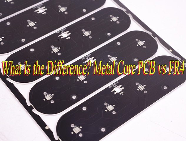
Top robotics 3D vision illuminator PCB manufacturers in Germany support lighting hardware that helps cameras capture stable depth data on reflective, dark, textured, or fast-moving objects. Choosing a supplier is not simply a matter of finding a company that can produce an aluminum PCB: the board must carry the LED load, remove heat, preserve optical consistency, fit the mechanical assembly, and arrive in time for camera and robot validation.

This guide helps German buyers assess manufacturers, prices, lead times, thermal capabilities, and sourcing routes for an illuminator PCB project. Buyers who also need a China manufacturing option can work with EBest Circuit, founded in 2006 and supported by 160 employees, more than 20 years of PCB and PCBA experience, 1,800+ customers across 40 countries, and a reported 97% on-time delivery rate. Its service combines PCB fabrication, component sourcing, PCBA, and testing. Send your Gerber files, BOM, target quantity, and required delivery date to sales@bestpcbs.com for an initial engineering review.
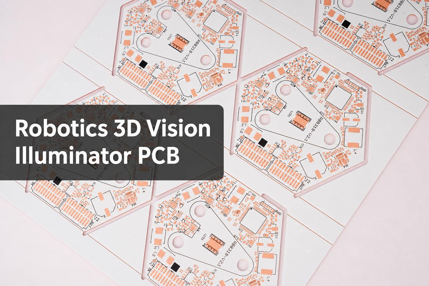
robotics 3D vision illuminator PCB

What Is a Robotics 3D Vision Illuminator PCB?

A 3D vision illuminator PCB is the circuit board that supports and drives the light source used by a robotic vision system. Depending on the sensing method, the illuminator may project infrared flood light, a structured pattern, a line, or synchronized pulses. The camera records the reflected light so that the vision system can calculate depth, locate parts, inspect surfaces, or guide a robot.

The PCB may look simple because LEDs dominate the visible side of the assembly, but its performance affects the complete optical system. Uneven LED current can create inconsistent brightness. Poor heat spreading can shift wavelength, reduce light output, shorten LED life, or distort calibration. Mechanical error can move the emitting surface away from the intended optical axis.

A buyer should therefore define the illuminator as an electro-optical assembly rather than as a generic LED board. Important inputs include:

  • illumination wavelength and optical power;
  • continuous, strobed, or pulsed operating mode;
  • LED quantity, package, current, and forward voltage;
  • required thermal resistance and maximum junction temperature;
  • board outline, mounting holes, connector position, and height restrictions;
  • driver topology, synchronization signals, and protection circuits;
  • camera distance, field of view, enclosure, lens, diffuser, or projector interface;
  • operating temperature, vibration, contamination, and service-life targets.

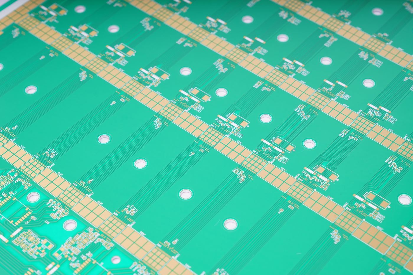
MCPCB is often suitable when the main challenge is removing heat from a compact LED array. A more complex illuminator may instead need a multilayer FR-4 board, a hybrid construction, or separate LED and control boards. The correct choice depends on the thermal path, signal requirements, component density, and mechanical design.
robotics 3D vision illuminator PCB

Top 3D Vision Illuminator PCB Manufacturers in Germany

The following companies are worth evaluating for thermal, high-reliability, prototype, or advanced PCB requirements in Germany. Their available services fit parts of an illuminator PCB project, but buyers should still confirm the MCPCB construction, PCBA scope, optical testing, available capacity, and production location for each quotation.

CONTAG AG, Berlin: CONTAG manufactures IMS and metal-core PCBs for LED, industrial, automotive, energy, and other thermally demanding applications. It also offers multilayer, HDI-SBU, high-frequency, flex, and rigid-flex boards. It is a strong candidate when an illuminator requires thermal engineering support, a fast German prototype, or a hybrid solution rather than a basic one-layer aluminum board.

Unimicron Germany GmbH, Geldern: Unimicron Germany offers multilayer boards up to 24 layers, HDI, high-frequency technology, metal-inlay solutions, IMS/heatsink technology, and other heat-management options. The company serves industrial and robotics applications, making it relevant when an illuminator combines power, control, communication, and thermal functions.

Becker & Müller Schaltungsdruck GmbH, Steinach: Becker & Müller provides in-house German production for prototypes and small batches and keeps IMS, FR-4, high-Tg, HF, and flex materials in stock. Its express service covers one- and two-sided boards, multilayers, and rigid-flex products. Buyers should ask which delivery option applies to the selected IMS material and stack-up.

Hotoprint Elektronik: Hotoprint manufactures PCBs in Germany, including multilayers up to 12 layers, flexible, rigid-flex, semiflex, and aluminum boards. Prototype and express services can begin from three working days, although the actual delivery date depends on the final MCPCB specification.

Leiton GmbH, Berlin: Leiton offers aluminum and copper IMS boards, German prototype production, an online calculator, and custom quotation support. Its Copper-IMS guide lists different lead-time options by layer count and shows which constructions require a direct enquiry.

This shortlist should begin a technical comparison, not end it. Some German companies focus mainly on bare PCBs, while a robotics buyer may need component sourcing, LED bin management, SMT assembly, programming, and functional testing. Ask each supplier to state exactly which operations are included and where they will be performed.

3D Vision Illuminator PCB Prices in Germany: What Buyers Should Compare

There is no reliable standard market price for a custom 3D vision illuminator PCB. Two boards with the same outline can have very different costs because price depends on material, panel utilization, copper weight, thermal dielectric, layer count, surface finish, tolerances, testing, quantity, and delivery speed.

For MCPCB prototypes, the main price drivers normally include:

  • aluminum versus copper base;
  • standard versus high-performance thermal dielectric;
  • one-layer, two-layer, or multilayer IMS construction;
  • board thickness and copper weight;
  • routed outline, slots, countersinks, or tight mechanical tolerances;
  • white solder mask, special marking, ENIG, or another nonstandard finish;
  • electrical test, documentation, and expedited manufacturing;
  • assembly quantity, LED package, placement density, and test coverage.

The lowest bare-board price is not always the lowest project cost. A cheaper board can become expensive if it needs a separate assembler, additional incoming inspection, repeated engineering communication, or rework after thermal testing. Conversely, paying a German prototype premium may be justified when local engineering contact or a very short iteration loop prevents a delayed robot trial.

Request quotations with the same manufacturing package and commercial assumptions. Each RFQ should specify quantity, panelization responsibility, material, copper, surface finish, test scope, tooling, delivery term, destination, and whether freight and tax are included. If PCBA is required, compare the BOM price, approved component sources, alternates, setup charges, programming, functional testing, and packaging separately.

A practical comparison uses at least three totals: prototype cost, landed cost, and cost of the next production quantity. This prevents an attractive sample price from hiding an unsuitable scale-up model.

What Lead Times Do German Manufacturers Offer for 3D Vision Illuminator MCPCBs?

German manufacturers publish useful benchmarks, but buyers must distinguish manufacturing time from delivery to the project site. The clock may begin only after data approval, material confirmation, DFM closure, and order release.

Leiton’s Copper-IMS technology document dated May 26, 2025, provides the clearest layer-specific public reference:

Copper-IMS constructionOnline calculationStandard on explicit enquiry
1 layer12 working days5 working days
2 layersNot availableFrom 4 working days
4-6 layersNot availableFrom 5 working days

These are Leiton’s manufacturing options for Copper-IMS boards. They are not universal German market lead times and do not automatically include assembly or shipping.

Eurocircuits lists five working days for bare boards and ten working days for assembled boards in its one-layer aluminum IMS pool. Because its PCB and assembly services are handled by factories in Germany and Hungary, buyers who require production specifically in Germany should confirm the assigned plant.

For project planning, separate the schedule into five parts:

  1. DFM review and clarification;
  2. special-material or component procurement;
  3. bare-board fabrication;
  4. assembly, programming, and functional testing;
  5. packing and transport to the German destination.

An advertised four- or five-day build does not help if a selected LED has a six-week procurement lead time. Send the complete BOM and approved-alternate policy early, and ask the supplier to state the ready-to-ship date rather than only the fabrication cycle.

Germany vs China for Robotics 3D Vision Illuminator PCB Manufacturing

Germany and China should not be compared through a single price or speed claim. The better choice depends on the development stage, specification stability, order quantity, communication needs, supply chain, and required manufacturing scope.

Buyer priorityGermanyChina
Local iterationStrong fitRemote review required
Integrated PCBASupplier-dependentCommonly available
Repeat-volume costQuote-dependentOften competitive
TransportShorter regional routeAdd freight and customs
Best useUrgent local prototypesIntegrated builds and scaling

A sensible sourcing strategy may use German manufacturing for an urgent local iteration and an approved China partner for integrated PCBA or repeat volume. Compare both options using the same material, stack-up, tolerances, surface finish, inspection scope, Incoterm, and delivery destination. If two sources will be used, approve the same golden sample before transfer.

Which MCPCB Process Capabilities Does EBest Circuit Offer for Robotics 3D Vision Illuminators?

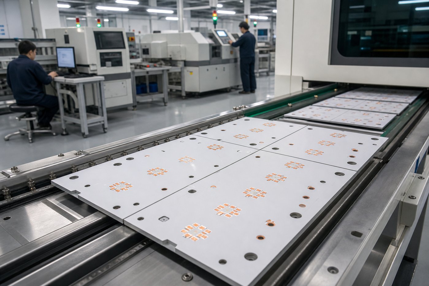
For illuminator projects, EBest Circuit supports the following metal-base PCB production ranges:

ItemStandard capabilitySpecial capability
Thermal conductivity1-3 W/(m·K)3-8 W/(m·K), subject to material confirmation
Board constructionSingle-sided, double-sided, single-sided two-circuit-layer aluminum/copper baseSingle-sided four-layer, subject to review
Thermoelectric separationCopper-base PCBCopper-aluminum composite construction
Inner-layer copper0.5-3 oz4 oz or above, subject to review
Outer-layer copper1-3 ozAbove 3 oz, subject to review
Processing thickness0.8-3.0 mm4.0 or 5.0 mm by material order; bendable aluminum: 0.4-1.0 mm
Maximum aluminum-board size480 × 1180 mmSingle-sided aluminum: 1600 × 480 mm

Final capability depends on the complete files, material availability, and quantity.
robotics 3D vision illuminator PCB

What Lead Times Does EBest Circuit Offer for Robotics 3D Vision Illuminator PCBs?

For standard MCPCB prototypes below one square meter, buyers can use the following fabrication times as an initial planning reference. The confirmed schedule depends on the released specification and current capacity.

MCPCB layersNormal serviceFastest service
1 layer4 days24 hours
2 layers14 days168 hours
4 layers21 daysConfirm before ordering

These timings apply to standard MCPCB prototypes with a total order area below one square meter. The standard specification uses conventional aluminum material, 0.8-2.0 mm board thickness, 0.5 oz or 2 oz copper, lead-free HASL, white solder mask, black silkscreen, and nominal thermal conductivity of 0.8 W/(m·K).

High-conductivity materials, thermoelectric-separation copper-base PCBs, OSP, special copper weights, unusual thicknesses, tight tolerances, and nonstandard panel requirements need a project-specific schedule. Production timing begins after the manufacturing data, material choice, technical questions, and commercial terms are confirmed.

The table covers bare-board production only. Component purchasing, PCBA, functional testing, packing, international freight, customs clearance, and delivery within Germany must be added separately. If the project deadline is fixed, send the files and required arrival date to sales@bestpcbs.com so EBest Circuit can check current capacity and provide a realistic ready-to-ship schedule.

EBest Circuit Engineering Case: Building a Robotics 3D Vision Illuminator PCB

In a robotics 3D vision system, the illuminator must project repeatable light while the camera captures depth information. If heat builds up unevenly beneath the LED array, brightness can drift across the field of view and make optical calibration less stable. The PCB therefore acts as part of the lighting system, not just as a carrier for LEDs.

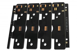
For one German illuminator project, EBest Circuit manufactured 180 pieces of a single-sided, two-circuit-layer thermoelectric-separation copper-base PCB. Its direct thermal path moved heat from the LED mounting area into the 1.5 mm copper base, while the isolated circuit layer carried power to the emitters. The specified 3 W/(m·K) material and 1 oz / 1 oz copper were selected to balance heat removal, current distribution, and the required 1.6 mm ±10% finished thickness.

The confirmed production specification was:

  • 1.5 mm copper base;
  • 1 oz / 1 oz copper;
  • thermal conductivity of 3 W/(m·K);
  • finished board thickness of 1.6 mm ±10%;
  • white solder mask and black silkscreen;
  • OSP surface finish;
  • delivery according to the customer’s panel drawing, with each individual board retaining its specified process rails.

White solder mask kept the LED side visually clean, black legend made polarity and assembly marks easy to identify, and OSP provided a flat surface for LED soldering. The boards were delivered in the customer’s released panel format with the required process rails, allowing the panels to enter LED assembly without repanelization.

Before production, the customer approved the final board configuration and panel format. The completed 180-piece lot was supplied with the requested COC and electrical test report. The German team therefore received one consistent board build for LED assembly and later camera-and-illuminator validation, without having to reconcile different thermal, mechanical, and panel specifications after delivery.

Why Choose EBest Circuit for 3D Vision Illuminator PCB Manufacturing?

EBest Circuit is a China-based PCB and PCBA manufacturing partner serving German and international buyers. Founded in 2006, the company has more than 20 years of industry experience, 160 employees, 1,800+ customers across 40 countries, and a reported 97% on-time delivery rate. It is most relevant when the project needs more than a bare-board price.

Technical support around the buyer: One sales contact is supported by three technical team members. DFM review, BOM optimization, and process-fit suggestions are available from engineers with long PCB and PCBA experience.

One project scope from board to test: PCB fabrication, component sourcing, PCBA, and customer-defined testing can be coordinated together, reducing handoffs between unrelated suppliers.

Prototype and low-volume support: Engineering samples and small batches help teams verify thermal behavior, mechanical fit, assembly, and optical performance before scaling.

Factory and supply-chain coverage: In-house PCB and PCBA resources are supported by more than 1,000 supply-chain partners, helping coordinate materials, components, quality controls, and delivery.

Traceability and quality systems: The digital workshop can trace material and product batches, production cycles, and progress. Available quality certifications include ISO 9001, ISO 13485, IATF 16949, and AS9100D.

A German manufacturer may still be preferable when physical production in Germany or immediate local iteration is mandatory. EBest Circuit is a stronger candidate when the buyer values integrated China sourcing, technical support, coordinated PCBA, traceability, and a route from prototypes to repeat production.

What Should You Send EBest Circuit for a 3D Vision Illuminator PCB Quote?

A first quotation does not need a perfect document package. To let EBest Circuit understand the project and identify missing information, start with five essentials:

  • your Gerber or ODB++ data, plus the board outline;
  • the LED or PCBA BOM if assembly is required;
  • prototype and expected production quantities;
  • known thermal targets, such as base material, conductivity, copper weight, or heatsink interface;
  • the German delivery location and the date the boards or assemblies are needed.

If your files are not complete yet, that is fine. Send what you have, and the engineering team will identify the few details needed next to evaluate price, manufacturability, thermal performance, and lead time. You do not need to prepare the full production package before requesting an initial review.

Email the available files to sales@bestpcbs.com and state that the request is for a robotics 3D vision illuminator PCB. EBest Circuit will review the current design, explain any information still needed, and prepare the quotation around your actual development stage.

FAQs About Robotics 3D Vision Illuminator PCB

Should a 3D vision illuminator use an aluminum or copper-base PCB?

Aluminum MCPCB is often suitable for cost-controlled LED heat spreading. Copper-base and thermoelectric-separation constructions can provide a more direct thermal path for higher heat density or tighter thermal targets. The right choice depends on LED power, pulse conditions, dielectric performance, mechanical structure, and the heatsink interface.

Can German manufacturers provide fast MCPCB prototypes?

Yes. Some German suppliers offer express or short prototype services. Leiton lists a five-working-day option for a one-layer Copper-IMS construction by direct enquiry, while more complex constructions require confirmation. Always check when the production clock begins and whether assembly and transport are included.

What should buyers compare besides the quoted PCB price?

Compare the metal base, dielectric, thermal conductivity, copper weight, board thickness, surface finish, tolerances, electrical test, documentation, tooling, panel delivery format, freight, and tax. For PCBA, also compare component sources, assembly setup, programming, functional testing, and approved alternatives.

Does EBest Circuit manufacture thermoelectric-separation copper-base PCBs?

Yes. EBest Circuit manufactures thermoelectric-separation copper-base PCBs. One completed German customer order used a single-sided, two-circuit-layer construction with a 1.5 mm copper base, 1 oz / 1 oz copper, 3 W/(m·K) thermal conductivity, OSP, and a finished thickness of 1.6 mm ±10%.

How can a German buyer reduce risk when sourcing an illuminator PCB from China?

Release a complete manufacturing package, approve the production data before fabrication, define acceptable materials and substitutions, agree on inspection and test reports, confirm the shipping term, and approve the pilot or golden sample before repeat production. These controls make the comparison more reliable than selecting a supplier by unit price alone.

Have a robotics 3D vision illuminator PCB ready for review? Email the available files, quantity, thermal requirements, and German delivery target to sales@bestpcbs.com. EBest Circuit will check the design, clarify the key manufacturing decisions, and respond with a quotation and project-specific schedule.

You may also like

Line Tracing Robot PCB Board Design, Manufacturing and Assembly Guide

August 17th, 2026

A line tracing robot PCB board must read optical contrast while two motors generate electrical noise, then convert those readings into stable steering commands. Production readiness depends on four controlled relationships: sensor geometry to the chassis, motor current to the power network, firmware to the hardware revision, and functional-test limits to the finished assembly.

Line tracing robot PCB board design manufacturing and assembly

Are you worried about your line tracing robot PCB board project?

  • Will sensor height, pitch, or alignment changes after assembly make a proven prototype track inconsistently?
  • Could motor startup, reversal, or stall current reset the MCU or corrupt the optical sensor readings?
  • Will mismatched PCB, BOM, firmware, and test revisions delay the quotation or create avoidable rework in production?

With 20 years of PCB and PCBA manufacturing experience, EBest Circuit provides one-stop support from production-data review through assembly and functional-test preparation.

  • Protect installed sensor geometry: Submit the PCB outline, sensor locations, mounting-hole datums, wheel-axis reference, and target sensor-to-track height. We review these controlled relationships with the fabrication and assembly data before production release, helping your team catch drawing conflicts before boards are built.
  • Control motor-power interference: Provide the battery range, motor running and stall current, driver part number, copper requirements, and critical sensor or reset limits. Our engineering review checks high-current paths, driver thermal features, decoupling placement, return paths, and test access so the prototype build can be evaluated under realistic motor transients.
  • Keep production inputs aligned: Release identified revisions of the Gerber or ODB++, fabrication drawing, BOM, centroid file, assembly drawing, firmware, calibration method, and functional-test limits. We compare the package before sourcing and assembly, then raise conflicts for approval rather than guessing at missing requirements.

Ready to start your line tracing robot PCB board project? Send your design files, BOM, quantities, stackup, firmware or programming scope, and test requirements to sales@bestpcbs.com for an engineering review and quotation.

What Does a Line Tracing Robot PCB Board Control?

The board measures the line position and converts the position error into separate left- and right-motor commands. A typical signal path is infrared emitter, photodetector, analog or timed input, MCU calculation, PWM output, motor driver, and motor. The PCB must support each interface without allowing the motor-current path to disturb the sensor reference.

Sensor channels first require calibration because emitter output, detector response, height, and track reflectivity vary. Firmware can normalize the channels, assign each sensor a position, and calculate a weighted line location. The difference between that location and the target center becomes the steering error. A proportional or PID-style routine then adjusts the two motor commands.

Freeze the operating behavior before schematic release. Define what happens when the line is lost, all channels saturate, a junction covers several sensors, a motor stalls, or battery voltage falls. These conditions determine MCU resources, fault inputs, driver selection, memory use, and factory-test coverage. A dedicated IR sensor PCB design review can support the emitter, detector, and receiver-interface decisions.

Should a Line Tracing Robot Use One PCB or Separate Control and Sensor PCBs?

Use one PCB for a compact robot with fixed sensor geometry; split the sensor and control circuits when the sensor bar must move, be replaced, or support several chassis variants. This is primarily a mechanical, service, and signal-integrity decision—not a preference for fewer or more boards.

  • Choose one PCB: The sensor height and forward offset are fixed, the board fits the chassis, and removing a cable and connector improves cost and reliability.
  • Choose two PCBs: The sensor bar needs independent height adjustment, is exposed to impact or dirt, or must be reused with different controller and motor configurations.
  • Control the interconnect: Specify connector family, pinout, cable length, retention, bend direction, current rating, shielding or ground conductors, and assembly orientation.
  • Share one datum system: Dimension the sensor centerline, wheel axis, mounting holes, and chassis references from matching origins on the PCB and mechanical drawings.

For a split design, keep local sensor filtering and any required analog reference close to the detector array. Do not route sensitive sensor outputs beside motor leads in the same cable without reviewing return paths and coupling. Prototype the complete cable and connector arrangement because a sensor board that works on a bench can become noisy after installation beside the motors.

How Does Sensor Placement Affect Line Tracing Robot Tracking Accuracy?

Installed sensor pitch, height, forward offset, and tilt determine what the control algorithm can measure. A layout may be electrically correct yet track poorly if the assembled array sits outside the optical range or moves relative to the wheel axis.

Choose the sensor-array width and channel pitch from the actual line width, minimum curve radius, target speed, and required steering resolution. Sensors placed too far apart can leave gaps in position information, while an unnecessarily tight pitch adds channels without correcting poor mechanical alignment. Evaluate the intended track materials because dark and light surfaces can produce different contrast margins.

Control sensor height from the running surface rather than from the bare PCB alone. Wheel diameter, tire compression, spacers, solder-joint height, board thickness, and chassis tolerance can all change the installed distance. Put the sensor centerline, wheel axis, and mounting holes on one mechanical datum system so PCB and chassis drawings cannot define conflicting positions.

Forward offset also changes steering behavior. A larger distance between the sensor array and wheel axis gives the controller earlier information about a curve, but it can amplify mechanical error and require different control tuning. Confirm the offset on the assembled robot instead of relying only on PCB dimensions.

Finally, keep board edges, fasteners, tall components, covers, and cable shadows outside the optical field. Define clean handling and inspection for emitter and detector windows, then verify the complete assembly under the expected ambient light—not only under controlled bench lighting.

How Should Sensor, MCU and Motor Driver Circuits Be Arranged on the PCB?

Partition the layout into a quiet sensor zone, a digital control zone, and a compact motor-power zone. Component placement should control current paths before detailed routing begins.

  • Place the sensor front end: Keep receiver filters, pull resistors, reference components, and any analog conditioning close to the sensor inputs. Protect these nodes from motor outputs, switching nodes, PWM traces, and high-current connector pins.
  • Group the MCU support circuit: Place clock, reset, boot, and local bypass components near their assigned MCU pins. Keep the programming interface accessible without routing it through the optical sensing area.
  • Compact the motor-power loop: Place the motor driver beside its high-frequency bypass capacitors and motor connector. Minimize the loop formed by the supply capacitor, driver power stage, motor output, and return path.
  • Control return current: Maintain a continuous signal reference where practical and use component placement to keep motor current away from sensor and MCU returns. Avoid arbitrary ground splits that force signals to cross gaps or take longer return paths.
  • Design the thermal path: Match exposed-pad copper, thermal vias, solder-mask openings, and paste apertures to the driver package and expected power loss. Confirm that the proposed structure can be fabricated, printed, reflowed, and inspected consistently.
  • Reserve test access: Provide reachable points for battery input, regulated rails, ground, reset, programming, driver fault, and representative sensor channels. Check fixture approach in the mechanical model so probes cannot collide with wheels, connectors, covers, or the sensor field.

How Can a Line Tracing Robot PCB Reduce Motor Noise and Power Instability?

Design the power network for motor start, reversal, braking, and stall rather than nominal running current. Size the connector, protection device, copper path, driver, regulator, and capacitance from the verified motor and battery limits with engineering margin.

Keep each switching-current loop short and place driver bypass components at the specified power pins. Do not share narrow return paths between motors and sensors. Separate motor outputs from sensor traces and oscillators, and decouple the MCU and sensor rail locally.

Validate the assembled prototype with an oscilloscope during start, stop, reversal, and stall-current limiting. Monitor battery input, regulated rails, MCU reset, sensor reference, and driver fault. A stable bench supply at idle does not prove the board will remain stable on the robot.

Which Line Tracing Robot PCB Board Specifications Should Be Confirmed Before Production?

Confirm the complete board construction and acceptance requirements in one controlled fabrication drawing before production. The drawing must agree with the Gerber or ODB++ data; conflicting notes create quotation delays and force the manufacturer to request clarification.

  • Board construction: State layer count, material family, finished thickness, stackup, copper weight by layer, and any controlled-impedance requirement.
  • Fabrication geometry: State minimum trace and spacing, finished-hole sizes, annular-ring expectations, routed slots, cutouts, castellations if used, and the finished outline tolerance.
  • Surface requirements: Specify the surface finish, solder-mask color and sides, legend color and sides, carbon or other special finishes, and areas that must remain free of mask or legend.
  • Mechanical controls: Identify the datum scheme, mounting-hole locations, sensor-edge relationship, connector position, profiling method, and any thickness or flatness constraint that affects the chassis.
  • Electrical acceptance: Define bare-board electrical testing, impedance coupons when applicable, netlist source, and any special isolation or high-current checks.
  • Panel and marking data: Define panel size or permit the manufacturer to propose it, then state tooling holes, fiducials, breakaway method, board identification, date code, and traceability needs.

The supplied EBest capability workbook lists general FR-4 references including up to 10 layers, 4/4 mil line and spacing with 1 oz copper, and a 0.2 mm minimum finished hole. These figures define review boundaries, not recommended values for every robot PCB. Select the released rules from motor current, voltage drop, annular-ring margin, board stiffness, routing density, assembly yield, and repeat-order stability; submit tighter features for engineering confirmation before quotation.

Which Components Require Special Controls During Line Tracing Robot PCB Assembly?

Optical sensors, thermal-pad motor drivers, polarized parts, connectors, and programming interfaces need explicit assembly controls. Their orientation, height, placement, or soldering can determine system function even when general workmanship is acceptable.

  • Optical sensors: Control the exact manufacturer part number, orientation, mounting height, coplanarity, window cleanliness, and any light barrier or cover that changes the field of view.
  • Motor drivers: Follow the component land pattern, thermal-pad via design, paste-window recommendation, polarity marking, and reflow limits; verify exposed-pad soldering with the agreed inspection method.
  • Polarized parts: Make diode, electrolytic-capacitor, LED, IC, and connector polarity unambiguous in the centroid file, assembly drawing, silkscreen, and first-article inspection.
  • Mechanical connectors: Check mating direction, latch access, cable exit, solder-joint support, insertion force, and clearance from wheels, batteries, and covers.
  • Programming interfaces: Reserve probe access and define pad finish, pitch, datum, keepout, and fixture approach so programming does not rely on hand-held wires.

Supply exact manufacturer part numbers, approved alternatives, centroid data, assembly drawings, and variant rules. A substitute optical sensor can change spectral response or package height even when its footprint fits; a substitute motor driver can change current limiting, decay behavior, pin functions, or thermal needs. Require approval before either part is changed.

Line tracing robot PCB assembly component and placement inspection

How Is a Line Tracing Robot PCB Board Manufactured and Assembled?

A line tracing robot PCB board moves through controlled data review, bare-board fabrication, assembly, inspection, programming, calibration, and functional testing. Each stage must use the same approved hardware, BOM, firmware, and test revisions.

  1. Review the production data: Compare Gerber or ODB++, drill files, fabrication notes, stackup, BOM, centroid data, assembly drawings, panel requirements, firmware, and test instructions. Resolve conflicting revisions, missing polarity, unsupported components, and unclear tolerances before material is released.
  2. Fabricate the bare PCB: Image and etch the copper layers, laminate multilayer constructions when required, drill and plate the holes, apply solder mask and legend, add the specified surface finish, and profile the board outline.
  3. Verify the bare board: Complete electrical testing against the supplied netlist and inspect dimensions, holes, slots, finish, markings, and workmanship. Controlled-impedance designs also require the agreed coupon and measurement records.
  4. Prepare the assembly line: Verify the released BOM and PCB revision, inspect incoming components, load the approved placement program, confirm stencil and paste requirements, and check feeder setup against polarity and package data.
  5. Place and solder components: Print solder paste, inspect the deposits when SPI is specified, place surface-mount parts, and run the validated reflow profile. Solder through-hole motor connectors, switches, or battery terminals in the specified secondary process.
  6. Inspect the assembled PCBA: Use AOI and appropriate manual or X-ray inspection to check presence, polarity, alignment, solder joints, exposed pads, and hidden connections. Record and disposition defects instead of passing reworked boards without traceability.
  7. Program and calibrate the board: Load the approved firmware, verify its checksum, apply configuration data, and expose every sensor channel to the defined light and dark references. Store or record calibration values according to the released method.
  8. Complete functional testing: Check input power, regulated rails, MCU operation, every sensor channel, left and right motor outputs, driver faults, and protection behavior against written limits. SPI and AOI confirm process conditions, but only functional testing demonstrates that the programmed assembly can control the robot.

How Should a Line Tracing Robot PCB Board Be Functionally Tested?

Functional testing must verify the programmed PCBA from power input through sensor response, motor control, fault handling, and real tracking behavior. Bare-board electrical test and AOI remain necessary, but they cannot prove that the finished assembly controls the robot correctly.

  1. Confirm the tested configuration: Read the PCB revision, BOM variant, firmware checksum, configuration version, and unit or lot identifier. Test only combinations approved in the hardware-firmware compatibility matrix.
  2. Measure power and startup: Apply the specified input range with current limiting, then check input current, regulated rails, reset behavior, and startup stability. Include polarity, undervoltage, or other protection functions only when they are part of the released design.
  3. Test sensors and calibration: Apply controlled light and dark references to every channel, confirm channel order, and compare readings with written limits. Run calibration at the specified sensor height and ambient-light condition, then verify that stored values can be recalled after a power cycle.
  4. Exercise motors and faults: Test left and right outputs independently with the specified motors or validated loads. Verify direction, PWM response, braking or coast behavior, current limiting, connector pinout, and driver-fault reporting; apply only safe fault conditions defined by the test plan.
  5. Run the assembled robot: Test with the released battery, motors, wheels, sensor height, axle offset, and cable routing. Use representative straight lines, curves, transitions, and line-loss conditions at the target speed so mechanical and control interactions are included.
  6. Save the acceptance record: Record measured values, limits, pass or fail status, firmware checksum, fixture revision, unit or lot identity, and rework status. This evidence must distinguish a programming, calibration, assembly, or component failure if the unit is investigated later.
Line tracing robot PCB board functional testing on a controlled track

How Can a Line Tracing Robot PCB Prototype Be Prepared for Volume Production?

Prepare a line tracing robot PCB prototype for volume production by replacing every temporary build decision with released data, repeatable tooling, and measurable acceptance criteria. A prototype that follows a track once is not yet a production baseline; the team must prove that the PCB, components, assembly process, firmware, calibration, and final robot mechanics can be reproduced without individual hand adjustment.

  • Remove prototype-only hardware: Replace flying wires, plug-in development modules, hand-soldered jumpers, temporary connectors, and manually added capacitors with documented schematic and PCB changes. If a modification remains necessary, include it in the controlled design rather than leaving it as an operator instruction.
  • Freeze compatible revisions: Assign released revisions to the schematic, PCB data, fabrication drawing, BOM, centroid file, assembly drawing, firmware, mechanical drawing, calibration method, and test specification. A compatibility matrix should identify which firmware and BOM variant belongs to each PCB revision.
  • Confirm component availability: Review optical sensors, MCU, motor driver, regulator, connectors, and other critical parts for lifecycle status, package consistency, lead time, minimum order quantity, and approved alternatives. Test any substitute that can change sensor response, component height, current limiting, pinout, or thermal behavior before adding it to the BOM.
  • Complete DFM and assembly review: Confirm trace and hole rules, annular rings, solder-mask clearances, copper balance, component spacing, polarity markings, paste apertures, thermal-pad design, connector access, and board-edge clearances. Resolve exceptions before the production panel and stencil are released.
  • Prepare panel and machine features: Add panel fiducials, tooling holes, breakaway rails, board identification, and a depaneling method that does not bend the sensor area or damage edge-mounted connectors. Verify that panel orientation supports paste printing, placement, inspection, soldering, and fixture loading.
  • Replace manual setup with fixtures: Provide stable access for programming, power, ground, reset, representative sensor channels, motor outputs, and driver faults. Calibration fixtures must reproduce the specified sensor height, optical reference, ambient-light condition, and board orientation instead of relying on an operator holding a target by hand.
  • Run a production-representative pilot build: Use the intended PCB panel, stencil, placement program, reflow profile, through-hole process, programming file, calibration routine, and functional-test limits. Include the released motors, battery range, cable routing, sensor-to-track height, and chassis datums when verifying complete tracking behavior.
  • Close defects before scaling quantity: Record solder defects, programming failures, calibration outliers, motor-channel faults, tracking failures, rework time, and component losses by cause. Correct the design or process, update every affected file, and repeat the necessary tests instead of treating successful rework as proof that the original process is ready.
  • Approve the production baseline: Retain the accepted first article or golden sample with its PCB revision, BOM, firmware checksum, calibration data, fixture revision, and test record. Repeat orders should use this controlled baseline, with customer approval and defined retesting for subsequent engineering changes.

Before releasing a larger order, require evidence that the pilot build used production-intent materials and processes, that every unit passed the written acceptance limits, and that open deviations have owners and closure dates. This prevents a low prototype price from turning into recurring rework, inconsistent tracking performance, or an avoidable schedule delay during volume production.

What Files and Specifications Are Required for a Line Tracing Robot PCB Board Quote?

A complete quotation package must define fabrication, assembly, sourcing, programming, calibration, and testing scope. Gerber files alone cannot describe a production-ready PCBA.

  • PCB data: Gerber and drill files or agreed ODB++, fabrication drawing, and stackup requirements.
  • Assembly data: BOM, centroid file, assembly drawings, polarity, and approved alternatives.
  • Mechanical data: Outline, datums, sensor height, chassis relationship, and connector constraints.
  • Firmware data: Released binary, checksum, target, programming method, and protection settings.
  • Test data: Calibration references, loads, limits, fixture responsibility, and required records.
  • Order scope: Prototype and forecast quantities, supplied parts, packaging, and delivery destination.

How Should You Choose a Line Tracing Robot PCB Manufacturer?

Choose a manufacturer by the risks it can remove from your prototype-to-production transfer, not by PCB price alone. The supplier should show how its controls protect tracking performance, revision accuracy, component availability, and delivery consistency.

  • Protect the sensor geometry: Confirm that the manufacturer reviews sensor pitch, height references, board outline, mounting holes, and connector positions against the mechanical drawing before fabrication.
  • Prevent power-related redesigns: Ask for review of motor-current paths, copper requirements, driver thermal features, regulator loading, and test access before the first production panel is released.
  • Control component substitutions: Require approval before changing optical sensors, motor drivers, connectors, regulators, or other parts that can alter function, height, pinout, or thermal performance.
  • Keep every revision aligned: The quotation, fabrication data, BOM, centroid file, firmware, calibration method, and test procedure should identify compatible revisions. This reduces the risk of assembling the correct components on the wrong PCB version.
  • Define measurable acceptance: Request the proposed inspection, programming, calibration, and functional-test flow. The supplier should explain which results are recorded and how failed or reworked units remain traceable.
  • Evaluate production support: Look for useful DFM feedback, clear responsibility for fixtures and supplied parts, documented issue approval, and a repeat-order process that preserves approved materials and settings.

Why Choose EBest Circuit for Line Tracing Robot PCB Board Manufacturing?

EBest Circuit gives buyers one coordinated path from PCB data review to assembled, programmed, and tested line tracing robot boards. Keeping these activities within one project review helps reduce handoff errors and gives your engineering and purchasing teams one place to resolve production questions.

  • Reduce launch delays: PCB data, BOM, assembly files, mechanical constraints, programming requirements, and test expectations can be reviewed together before production begins.
  • Improve sourcing control: Exact parts and approved alternatives can be identified before purchase, with customer approval required for changes that may affect optical, motor-control, connector, or power performance.
  • Simplify supplier coordination: Fabrication, component sourcing, assembly, programming preparation, and production testing can be managed through one manufacturing project instead of separate uncontrolled handoffs.
  • Support prototype-to-volume transfer: The same released revisions, inspection requirements, calibration inputs, and functional-test criteria can follow the project from validation builds into repeat orders.
  • Match the board technology to the design: EBest Circuit, also known as Best Technology, supplies standard and multilayer FR-4 as well as HDI, high-Tg, heavy-copper, high-speed, impedance-controlled, flexible, rigid-flex, metal-core, ceramic, and high-frequency PCB constructions.
  • Review required compliance evidence: The supplied company information lists ISO 9001:2015, ISO 13485:2016, IATF 16949, AS9100D, UL, RoHS, and REACH credentials. Request the documents and scope applicable to your product and destination during quotation review.

Frequently Asked Questions About Line Tracing Robot PCB Boards

Q1: How should hardware revisions be marked?

A1: Put a readable revision on the PCB and define the required lot or serial identifier. Ensure it remains visible after assembly.

Q2: Does the robot need wheel encoders?

A2: Not every design needs encoders. Add them when wheel-speed feedback or stall detection justifies the extra inputs and firmware.

Q3: How should optical sensors be protected?

A3: Define clean handling, inspection, and packaging for every optical surface. Prevent residue, abrasion, and packaging pressure on the windows.

Q4: Can customer-supplied motors and batteries be included?

A4: The integration scope must be reviewed before quotation. Provide specifications, connectors, safety constraints, drawings, and test limits.

Q5: Should the assembly receive conformal coating?

A5: Use coating only when the environment and component set justify it. Define optical, connector, and test-point keepouts.

Q6: How large should the validation build be?

A6: Use enough units to exercise the real assembly, programming, calibration, and test process. Set the quantity from validation objectives and process risk.

Q7: How can motor wiring mistakes be prevented?

A7: Use keyed connectors, clear pin numbering, and visible left-right identification. Confirm the mating cable orientation in the assembly drawing.

Q8: Can one PCB support different sensors or motors?

A8: Yes, when every variant is deliberately designed and documented. Control footprints, DNP options, BOMs, firmware, and tests separately.

Q9: What should a golden sample control?

A9: Bind it to approved hardware, BOM, firmware, calibration, and test revisions. Drawings still govern dimensions and hidden requirements.

Q10: What packaging details should be specified?

A10: Define ESD protection, board separation, optical protection, labels, and pack quantity. Prevent parts from rubbing or loading one another in transit.

Conclusion

Turn your working robot prototype into a repeatable production build before unresolved sensor, motor, firmware, or test details become schedule and rework costs. Send EBest Circuit your Gerber or ODB++ data, BOM, mechanical drawing, target quantities, firmware and calibration scope, and functional-test requirements. Our team can review the manufacturing package, identify the questions that must be closed before production, and prepare a quotation for your line tracing robot PCB board project. Contact sales@bestpcbs.com to start the review.

You may also like

Custom Servo Driver Board Manufacturing and PCB Assembly for AI Robot Hardware

August 14th, 2026

A servo driver board turns an AI robot controller’s motion commands into stable, synchronized actuator movement. A reliable custom design must match the servo interface, simultaneous current demand, control timing, connector system, PCB layout and test strategy; a simple bank of headers is not enough.

The scope covers PWM and serial-bus servo interfaces for robot hardware. Industrial AC servo drives require a separate motor-specific power-stage and control design.

Servo driver board for multi-axis AI robot hardware on a laboratory workbench

What Is a Servo Driver Board in AI Robot Hardware?

A servo driver board connects the robot processor, power source and servo actuators. Its exact role depends on the actuator and command architecture.

Its core functions are to distribute power, route or generate control signals, monitor required feedback and provide the necessary protection and connectors.

This interface must control timing, supply stability, contact reliability and logic integrity. The robot processor cannot correct these board-level failures after they occur.

How Does a Servo Driver Board Control Robot Motion?

The board converts a position, velocity or torque request into the electrical command format expected by each actuator. For a PWM servo, command timing encodes the requested position. For an addressed serial servo, a data packet identifies the actuator and target. Closed-loop industrial drives add current and feedback processing, so they require a different power and control architecture.

Evaluate the complete path under coordinated load; a single unloaded servo will not expose bus timing errors, voltage sag or corrupted feedback.

  • Deterministic updates: Schedule channel updates so simultaneous joints do not receive stale or irregular commands.
  • Safe startup: Hold outputs in a defined state until power rails, firmware and communication are ready.
  • Fault containment: Prevent one shorted cable or failed actuator from disabling unrelated control electronics when required by the system safety analysis.
  • Feedback integrity: Keep encoder, current, temperature and status paths away from noisy power switching loops.

How Do You Choose a Servo Driver Board for a Multi-Axis AI Robot?

Choose the board architecture from the actuator interface, peak simultaneous load and required motion coordination. Channel count by itself is not enough. Two boards with the same number of outputs can behave very differently when several joints accelerate together, when cables are long, or when the robot must recover safely after a fault.

Document these seven inputs before selecting the circuit architecture or connector count:

  • Actuator compatibility: Record every servo part number, supply range, command protocol, logic level and pinout. Confirm the interface from the actuator datasheet and, where possible, a known-good signal capture; a connector match alone does not prove electrical compatibility.
  • Axis count and update timing: Define the installed channels, axes that move together, required update period and worst-case bus latency. A board with enough outputs can still produce visible jitter if commands are delayed or updated unevenly.
  • Simultaneous power demand: Base the input rail, branch distribution and connector current rating on the real acceleration, reversal and holding profile. Normal running current can hide the short peaks that cause brownouts, resets or overheated contacts.
  • Feedback and diagnostics: Specify whether the controller needs position, current, temperature, status or fault data from each actuator. Confirm the required bandwidth and response to missing or invalid feedback before choosing a one-way PWM or bidirectional bus architecture.
  • Cable and connector limits: Control the mating part, pin sequence, wire gauge, cable length, retention method and mating-cycle requirement. These details affect voltage drop, signal integrity, serviceability and resistance to intermittent contact.
  • Startup and fault behavior: Define the output state during power-up, reset, undervoltage, overcurrent, watchdog timeout and communication loss. Decide whether one failed actuator or cable must remain isolated from the controller and other axes.
  • Mechanical and test integration: Check board outline, mounting, enclosure airflow, connector access, programming method and test-point access. Verify measurement and service access in the installed robot, because bench access may hide enclosure constraints.

Why Do Multiple Servos Jitter or Reset the Robot Controller?

Multi-servo jitter and controller resets usually begin with supply droop, shared return impedance, irregular command timing or EMI coupling. Diagnose these causes at the board while reproducing the loaded motion, not by replacing firmware or adding capacitors at random.

  • Reproduce the event: Run the exact joint combination, acceleration and mechanical load that causes the fault.
  • Measure at the load: Capture minimum rail voltage and transient duration at local connectors or test points with adequate bandwidth.
  • Correlate timing: Capture supply voltage, reset, command signal and fault output on the same time base.
  • Separate causes: Repeat with one actuator at a time, reduced acceleration and an alternate cable route to distinguish load current from coupling.
  • Verify the repair: Re-run the worst-case motion across the intended input-voltage and temperature conditions.

Also inspect shared connector pins, thin ground traces and long harness returns; transient current through these impedances can shift the local logic reference and trigger a reset.

How Should Power Integrity Be Designed for a Multi-Servo Driver Board?

Size and verify every element from the power source to the servo connector and return path under simultaneous motion. Use the real motion profile rather than channel count alone.

  • Model simultaneous current: Add the servos that can operate together, controller current and design margin; use stall current only for a credible operating or fault state.
  • Budget voltage drop: Calculate each source, protection, connector, copper, via, cable and return segment with Vdrop = I × R, then measure at the loaded connector.
  • Bulk energy: Place appropriately rated bulk capacitance where the servo rail enters and where a branch experiences a fast load step.
  • Local decoupling: Use the values specified by each controller, transceiver and power-device manufacturer, with short connections to the relevant supply and return pins.
  • Low-impedance distribution: Use copper geometry, layer transitions and connector contacts that match the calculated current and allowable temperature rise.
  • Rail separation: Keep noisy actuator current from flowing through the logic regulator’s sensitive supply and return path.
  • Protection coordination: Select reverse-polarity, surge, overcurrent and branch protection for the available source energy and credible harness faults.
  • Copper and stackup: Select FR4 copper weight and distribution from current, temperature rise, voltage drop and routing density; confirm spacing, vias, escape routing and manufacturability.

How Do PCB Layout, EMI and Thermal Design Affect Servo Board Reliability?

Coordinate switching-loop geometry, return paths, noise control and heat flow during PCB layout. One filter cannot correct poor routing after the layout is complete.

  • Shrink critical loops: Keep the source, switching device, load path, decoupling capacitor and return loop compact.
  • Preserve return paths: Avoid routing that cuts the reference plane beneath clocks, buses and sensitive measurements.
  • Partition by function: Separate power switching, logic, analog sensing and external interfaces while providing deliberate connection points between their returns.
  • Control coupling: Increase separation from noisy nodes, reduce long parallel runs and protect high-impedance signals.
  • Build a thermal path: Connect exposed pads to continuous copper and an appropriate thermal-via pattern, then measure the assembled board under the worst credible motion profile.
  • Record thermal conditions: Log input voltage, active channels, mechanical load, airflow, enclosure state, ambient temperature and soak time with every temperature result.

Compare component and board hot spots with the applicable device limits, derating policy and robot duty cycle.

How Does a Custom Servo Driver Board Prototype Validate Robot Performance?

Validate the prototype under representative multi-axis load; one unloaded servo is not sufficient release evidence. Use six verification gates:

  1. Design for observation: Add safe access to input, servo and logic rails, ground, reset, communication, command outputs and current measurement.
  2. Verify static safety: Check shorts, polarity and rail resistance, then perform the first power-up with a current-limited supply before connecting actuators.
  3. Validate one channel: Confirm signal format, connector pinout, direction, range and fault behavior with one known actuator.
  4. Increase concurrency: Add channels according to the real robot motion profile while logging minimum rail voltage, current and timing.
  5. Apply mechanical load: Test acceleration, reversal, holding and collision-recovery states that change actuator current.
  6. Record release evidence: Save waveforms, temperatures, firmware version, board revision, actuator list and pass limits.

What Must Be Controlled During Servo Driver Board PCB Assembly?

Assembly control must protect component identity, polarity, solder quality, connector alignment and thermal-pad integrity. Servo boards often combine fine-pitch logic, large capacitors, power packages and mechanically loaded connectors, so one uniform inspection method is insufficient.

Servo driver board PCB assembly undergoing automated optical inspection
  • BOM control: Lock manufacturer part numbers, approved alternates, package, ratings and do-not-substitute items.
  • Moisture handling: Follow the component and packaging requirements for moisture-sensitive devices before reflow.
  • Paste and reflow control: Match stencil apertures and the validated thermal profile to the component mix and exposed pads.
  • Polarity inspection: Verify diodes, electrolytic capacitors, IC orientation and connector pin-one features against controlled drawings.
  • Joint inspection: Use AOI for visible placement and solder features, then add X-ray where hidden joints or thermal pads create a real risk.
  • Connector mechanics: Check coplanarity, retention, insertion clearance and any hand-soldered or press-fit operation before functional test.
  • Revision control: Release matching fabrication, BOM, centroid and assembly files under one revision identifier.
  • Programming control: Define the image, checksum, security state, connector, fixture and pass record before assembly release.

Which Functional Tests Should Validate an AI Robot Servo Control Board?

Functional testing should verify power, every channel, communication, protection and loaded motion behavior against written limits. A power-on LED is only an initial observation; it does not prove channel timing, voltage margin or fault recovery.

AI robot servo control board functional testing with multiple servo actuators
Test Method
Input and rails Measure startup, steady state and worst-case transient at defined test points
All output channels Exercise each connector with a known load or validated simulator
Communication Test valid frames, timeout, missing device and bus recovery
Protection Apply controlled undervoltage, overload or disconnected-load conditions where safe
Loaded motion Run representative concurrent trajectories and mechanical loads
Programming and identity Read firmware, configuration, serial-number or revision identifiers

Set limits from actuator data, the control budget, safety analysis and system requirements. Use a protected fixture or simulator for unsafe fault tests and document its coverage limits.

How Do You Move a Servo Driver Board from Prototype to Production?

Release the design only after the board definition, approved parts, assembly controls and measurable acceptance limits are ready for repeat production. Confirm all eight requirements:

  1. Close prototype findings: Assign every electrical, thermal, communication and mechanical failure a root cause, corrective action and passing retest. Update the schematic, layout, BOM and firmware together so the released files match the tested board.
  2. Complete PCB DFM: Review the approved stackup, copper distribution, minimum geometry, drill and via structure, board outline, connector clearances, panelization and fabrication notes against the chosen manufacturer’s documented capabilities.
  3. Complete assembly and test DFM: Confirm package footprints, polarity marks, stencil requirements, fiducials, tool clearance, programming access and test-point size and spacing. The fixture must reach every required rail, interface and output without stressing connectors.
  4. Qualify the production BOM: Lock manufacturer part numbers for controllers, power devices, capacitors and connectors. Evaluate an alternate for electrical rating, pinout, package, thermal behavior, startup behavior and firmware compatibility before approval.
  5. Freeze production inputs: Issue matching Gerber or ODB++, drill, stackup, fabrication notes, BOM, centroid, assembly drawings, firmware image, programming instructions and functional-test specification under one revision.
  6. Build a production-intent pilot: Use the planned PCB construction, approved components, stencil, reflow process, programming method and test fixture. Temporary prototype wiring, hand-selected parts or laboratory-only setup must not hide transfer risks.
  7. Review pilot results: Classify fabrication, placement, soldering, programming and functional-test failures. Record rework and retest results, then verify rail voltage, timing, temperature and loaded multi-axis behavior against written limits before increasing quantity.
  8. Control post-release changes: Link every component, PCB, process, firmware or fixture change to an approval record and an affected-test plan. Repeat only the tests justified by the impact analysis, but never accept generic replacement equivalence without verification.

Why Choose EBest for Custom Servo Driver Board Manufacturing?

Reduce engineering handoffs, identify production risks earlier and keep the approved board and BOM aligned from prototype through repeat builds. These EBest Circuit services address those needs:

  • Resolve board-level risks before ordering volume: PCB design support can review power distribution, stackup, routing, connector placement and test access against the servo interface and motion-load requirements.
  • Validate the design with lower commitment: PCB prototyping and assembly services enable verification builds before the design moves to mass production.
  • Reduce uncontrolled BOM changes: Component sourcing and PCB assembly can work from the same approved manufacturer part numbers and flag alternatives that require engineering confirmation.
  • Match the PCB construction to the electrical load: EBest’s product scope includes FR4, multilayer, heavy-copper, high-Tg and impedance-controlled PCBs for project-specific stackup review.
  • Simplify prototype-to-production transfer: PCB design, prototype, sourcing, assembly and mass-production services can use one controlled set of fabrication, BOM, programming and test files.
  • Support supplier qualification: Use a defined PCB assembly manufacturer selection process to confirm sourcing responsibility, inspection, testing, traceability and change control. EBest lists IATF 16949, ISO 9001:2015, ISO 13485:2016, AS9100D, REACH, RoHS and UL credentials; confirm the certification and product-level documentation required for the specific robot program during quotation.

FAQs About Servo Driver Boards

Q1: What files should I send for a custom servo driver board quotation?

A1: Send the complete fabrication and assembly package. Include Gerber or ODB++, drill files, BOM, centroid data, assembly drawings, quantity, stackup, servo models, protocol, voltage, simultaneous-motion requirement, firmware method and functional test limits.

Q2: Can EBest assemble a customer-designed servo control PCB?

A2: Yes, EBest can fabricate and assemble a customer-designed board. The files still need engineering review for manufacturability, component availability and test readiness before release.

Q3: Can firmware be programmed during PCB assembly?

A3: Programming can be included with controlled inputs. Provide the firmware image, programming interface, security instructions and verification method, including the checksum or version readback that proves the correct image was loaded.

Q4: Does EBest provide a free DFM review before quotation?

A4: Yes, EBest offers a free DFM review for the submitted PCB and assembly package. The review can identify manufacturability issues involving stackup, copper geometry, drill and via choices, component footprints, assembly clearances and test access before production.

Q5: Which PCB constructions can be reviewed for a servo driver board?

A5: The appropriate construction depends on current, thermal, signal and mechanical requirements. EBest’s product scope includes FR4, multilayer, heavy-copper, high-Tg and impedance-controlled PCBs for project-specific review.

Q6: Can EBest support both bare PCB fabrication and complete PCB assembly?

A6: Yes, the service scope includes PCB fabrication, component sourcing and PCB assembly. Define whether the quotation requires bare boards, assembled boards, programming, functional testing or a combination of these services.

Q7: Which quality or compliance credentials should buyers confirm?

A7: Match the required certification or compliance document to the product and end-use program. EBest lists IATF 16949, ISO 9001:2015, ISO 13485:2016, AS9100D, REACH, RoHS and UL credentials; request the applicable current documentation during supplier qualification.

Q8: When is conformal coating appropriate for a robot servo board?

A8: Use conformal coating only when the environmental risk justifies it. Specify keep-out areas, connectors, test points and rework requirements; coating cannot compensate for inadequate spacing or enclosure design.

Q9: What information helps EBest provide a useful DFM review?

A9: Submit the manufacturing files together with the application’s electrical limits. Include Gerber or ODB++, stackup, BOM, centroid data, assembly drawings, servo models, voltage, simultaneous-load profile, connector constraints and required tests.

Q10: What records can accompany a servo driver board shipment?

A10: Define shipment records in the purchase specification. Request the inspection, programming, functional-test and traceability records needed for receiving acceptance before the order is released.

Conclusion

Ready to reduce manufacturing risk before ordering your servo driver board? Send your Gerber or ODB++, BOM, quantity, stackup, servo interface, simultaneous-load profile, assembly, programming and test requirements to sales@bestpcbs.com. Ask EBest for a free DFM review and quotation for your AI robot hardware project.

You may also like

PCB Robot Manufacturing Guide | Robot PCB and PCBA Assembly

July 27th, 2026

A PCB robot can mean a small robot built on a printed circuit board, a robot control board, or a PCB used inside a robotic system. For engineers and buyers, the real question is not only what the term means. The real question is whether the robot PCB can be manufactured, assembled, tested, and delivered without creating avoidable problems during prototype validation.

EBest Circuit (Best Technology) supports robot PCB and PCBA projects with PCB fabrication, component sourcing, SMT assembly, through-hole assembly, DFM review, inspection, testing coordination, and small-batch production. If your robotics project includes Gerber files, BOM, CPL, stackup notes, impedance requirements, assembly drawings, or test instructions, you can send them to sales@bestpcbs.com for engineering review before production starts.

pcb robot
Robot PCB manufacturing starts with a clear understanding of control, power, sensors, connectors, assembly, and testing requirements.

What Does PCB Robot Mean for Real Robotics Projects?

In real robotics projects, a PCB robot usually refers to the printed circuit board used inside a robot or robotic module. The board may control motors, read sensors, manage power, connect communication interfaces, or support firmware programming and testing.

The meaning can change by project type:

  • A student project may use a line follower robot PCB.
  • A mobile robot may use a motor control PCB.
  • An industrial robot may use controller, I/O, sensor, and power boards.
  • A robotic camera or inspection system may need high-speed signal routing.
  • A service robot may combine sensors, wireless modules, battery circuits, and compact connectors.

The risk is that a robot PCB is often judged only by whether the circuit works on paper. In production, the board also has to survive soldering, cable connection, vibration, current load, heat, enclosure limits, and repeated operation.

For this reason, a useful manufacturing review should connect the circuit files with the real working condition. A robot control board is not only a PCB layout. It is part of a moving product.

PCB Robot vs Robot PCB: Which Meaning Fits Your Project?

PCB robot and robot PCB are often used together, but they do not always describe the same thing.

PCB robot may describe:

  • A small robot built directly on a PCB
  • A foldable or structural PCB robot
  • A DIY robot board
  • A robotics-related printed circuit board
  • A robot used in PCB production

Robot PCB is usually clearer for manufacturing. It means a PCB used inside a robot system.

For EBest Circuit, the practical focus is robot PCB and robotics PCB manufacturing. The customer’s design team defines the circuit, firmware, MCU, sensor strategy, control logic, and robot function. Our role is to review whether the provided PCB and assembly files can move through fabrication, sourcing, SMT, inspection, testing, and packing reliably.

That distinction matters. If a customer asks us to create the full robot electronics design from scratch, that may go beyond our service scope. If the customer provides production files and needs manufacturing, assembly, DFM, BOM, and testing support, that is where EBest Circuit can help.

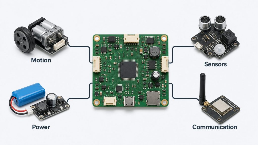
How a Robot PCB Connects Motion, Sensors, Power, and Communication

A robot PCB becomes valuable because it connects several demanding functions on one board.

pcb robot
A robot PCB often connects motion control, sensor input, power management, and communication interfaces on one board.

Motion control

Motor drivers, MOSFETs, relays, encoders, and connectors may carry current and receive fast control signals. If copper width, heat dissipation, solder joints, or connector strength are not reviewed, the robot may fail during movement rather than during simple bench testing.

Sensor input

Robotics boards often connect optical sensors, IR sensors, cameras, IMUs, encoders, ultrasonic sensors, pressure sensors, or current sensors. Sensor areas may be sensitive to connector direction, solder cleanliness, signal noise, and mechanical position.

Power management

Robots may use batteries, adapters, DC motors, regulators, charging circuits, and protection devices. A small power issue can cause reset, unstable motor behavior, overheating, or failed validation.

Communication

USB, CAN, UART, RS485, Ethernet, Wi-Fi, Bluetooth, or other interfaces may appear on the same board. If controlled impedance or differential routing is required, the stackup and impedance plan should be confirmed before fabrication.

This is why robot PCB manufacturing cannot be treated like a simple bare board order. The board must match the customer’s electrical files and the physical working environment.

PCB Design for Robotics: What Must Be Ready Before Manufacturing?

For PCB design for robotics, EBest Circuit does not replace the customer’s design team. However, before production starts, certain files must be clear enough for manufacturing.

The most useful customer file package includes:

  • Gerber or ODB++ files
  • Drill files
  • BOM
  • CPL or pick-and-place file
  • Assembly drawing
  • PCB drawing
  • Stackup requirement
  • Board thickness and tolerance
  • Copper thickness
  • Surface finish requirement
  • Impedance notes, if any
  • Firmware file, if programming is required
  • Test instructions
  • Packing notes

The problem is not only missing files. The bigger risk is inconsistency between files.

For example, a connector may face one direction in the assembly drawing but another direction in the CPL file. A BOM may list a component package that does not match the PCB footprint. A programming header may be present but blocked after assembly. A sensor may need edge alignment, but the panel design may make depaneling risky.

These are the kinds of issues that should be found before SMT starts, not after the customer receives the first prototype.
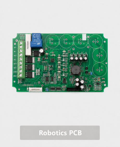
Robot Controller PCB Risks That Can Delay Prototype Validation

A robot controller PCB often becomes the first board the customer tests during bring-up, especially in a prototype circuit board assembly project. If it fails, the whole robot project slows down.
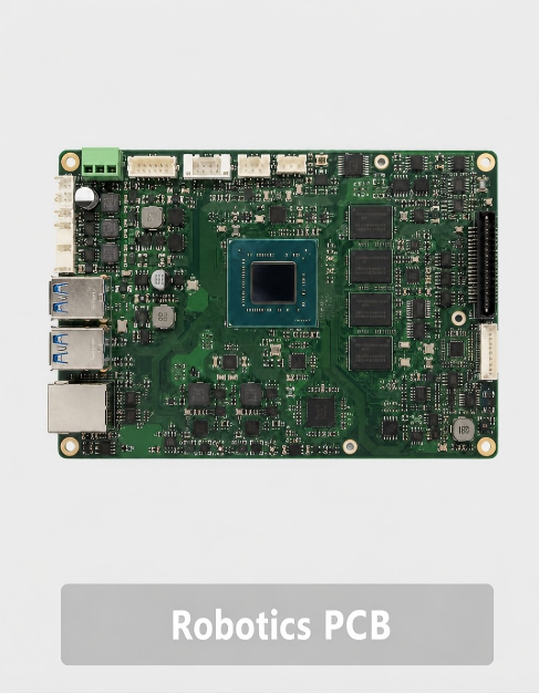
Common validation risks include:

  • Motor driver overheating
  • MCU or processor orientation errors
  • Unclear programming access
  • Sensor connector mismatch
  • Wrong polarity on power input
  • Weak solder joints on high-stress connectors
  • Insufficient copper for current paths
  • Missing or inaccessible test pads
  • BGA or QFN soldering defects
  • Board warpage or poor mechanical fit
  • Packing damage after assembly

A low-cost prototype can become expensive if debugging time is lost. Engineers may spend days checking firmware, motor drivers, sensors, or wiring before discovering the issue came from assembly, a wrong component, or an unclear production note.

EBest Circuit’s value is to catch practical manufacturing risks early. For robot controller PCB projects, our engineering review focuses on the details that affect whether the first assembled boards can enter customer testing smoothly.

How EBest Circuit Reduces Robot PCB Assembly Risks Before SMT

Robot PCB assembly is where many small file issues become real defects. Before SMT, EBest Circuit reviews the project as a complete build, not as separate documents.

pcb robot
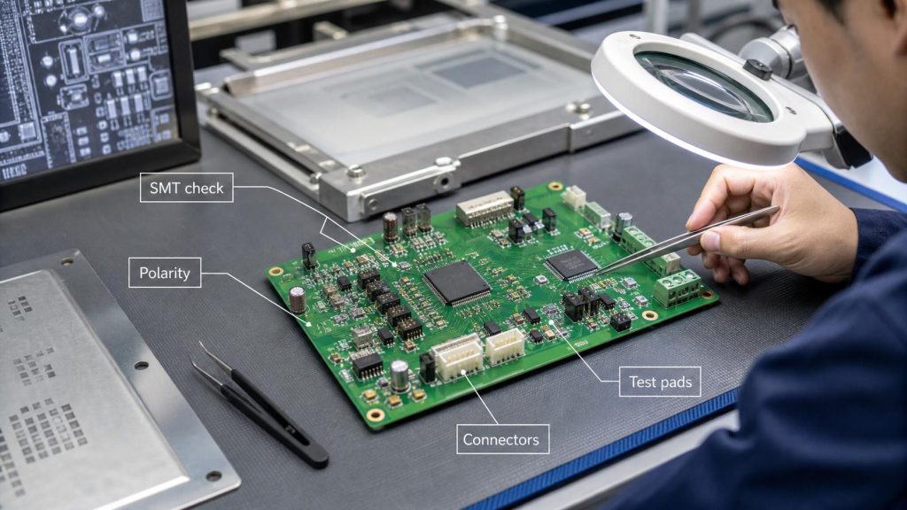
Before SMT, robot PCB assembly files should be checked for polarity, connector direction, test access, and process risks.

The review focuses on production risk:

  • Does the BOM match the PCB footprint?
  • Are connector directions clear?
  • Are polarity marks visible and consistent?
  • Are fine-pitch ICs suitable for the stencil and SMT process?
  • Does the panel support stable printing and placement?
  • Are BGA, QFN, or hidden solder joints expected?
  • Are through-hole parts and hand soldering notes clear?
  • Does the board need cleaning after assembly?
  • Is firmware programming required?
  • Does the customer define a functional test method?

This matters because robot PCBA projects often combine SMT parts, plug-in connectors, power parts, cables, programming interfaces, and test points. If one item is unclear, the board may still be assembled, but the customer may not be able to use it smoothly.

A good robot PCB assembly process is not only about placing components. It is about keeping the customer’s engineering intent visible until the board is packed and shipped.

Line Follower Robot PCB: Small Board, Real Manufacturing Risks

A line follower robot PCB is often used in education, competitions, and early robotics prototypes. It may look simple, but it still has real manufacturing risks.

Typical features include:

  • Microcontroller
  • Motor driver
  • IR sensor array
  • Battery input
  • Voltage regulator
  • Motor connectors
  • Programming header
  • LEDs or display
  • Mounting holes
  • Compact board outline

The main challenge is that the board is small, but the functional sensitivity is high.

If the sensor array is not positioned correctly, line detection may be unstable. If the motor current path is too narrow, heat or voltage drop may affect movement. If the battery connector or motor connector is weak, repeated plugging and movement may damage the solder joint. If test access is poor, debugging becomes slower.

For small robotics prototypes, EBest Circuit can review panelization, component direction, soldering process, connector strength, and inspection access before assembly. That helps the customer spend more time testing robot behavior and less time chasing avoidable production issues.

Robot PCB Manufacturing Details That Affect Reliability

Robot PCB manufacturing details can affect whether the board performs reliably after assembly.

Important reliability-related factors include:

  • Board thickness
  • Copper thickness
  • Material Tg
  • Via structure
  • Surface finish
  • Solder mask opening
  • Mounting hole plating
  • Connector pad strength
  • Thermal design around power parts
  • Controlled impedance for high-speed interfaces
  • Panel design for SMT
  • Electrical testing before assembly

For example, a robot board with motor drivers may need stronger attention to copper width, thermal relief, and high current PCB assembly requirements. A sensor board may need clean solder mask definition and stable connector placement. A compact controller with BGA or fine-pitch ICs may need better DFM review, AOI, and X-Ray planning.

EBest Circuit supports FR4 PCB, high-Tg PCB, HDI PCB, flex PCB, rigid-flex PCB, metal core PCB, ceramic PCB, heavy copper PCB, and impedance-controlled PCB projects. For robot PCB projects, the right process depends on the board’s current, density, mechanical space, and testing needs.

How Robotics PCBA Testing Helps Catch Problems Before Delivery

A robotics PCBA should be inspected and tested according to the project risk, with suitable PCB testing and assembly inspection methods. The purpose is not to make the process look complex. The purpose is to catch problems before the boards reach the customer’s test bench.

pcb robot
Robotics PCBA testing may include AOI, X-Ray, power-on checks, functional testing, and ESD-safe packing before delivery.

Possible inspection and test steps include:

  • Incoming material check
  • SPI after solder paste printing
  • AOI after reflow
  • X-Ray for BGA, QFN, or hidden solder joints
  • Visual inspection
  • Through-hole solder joint inspection
  • Bare PCB electrical test
  • Firmware programming, if customer provides firmware
  • Power-on check
  • Customer-defined functional test
  • Connector and polarity inspection
  • Final packing inspection

For robot PCBA projects, test points should be planned carefully. Power, ground, programming, communication, motor output, and key sensor signals may need accessible pads if the customer expects production testing.

A robot PCB should not only pass visual inspection. It should arrive ready for bring-up, movement testing, sensor connection, and next-stage validation.

PCB Robot Manufacturing Case Study for a USA Robotics Project

A USA customer needed a small batch of robot controller PCB assemblies for an indoor mobile robot prototype. The project was used for motion control validation before the customer moved toward pilot production.

Project requirements

  • Customer region: USA
  • Application: Indoor mobile robot controller
  • Quantity: 30 pcs prototype PCBA
  • PCB type: 4-layer FR4 robot controller PCB
  • Material: High-Tg FR4
  • Finished thickness: 1.6mm +/-10%
  • Copper thickness: 1oz finished outer copper
  • Surface finish: ENIG
  • Assembly: SMT + through-hole connectors
  • Main areas: MCU, motor driver, sensor connectors, power input, programming header
  • Test: Power-on check, connector inspection, customer-defined functional test points
  • Packing: Single-board ESD packaging after assembly

Main risks

  • The motor driver area needed stable soldering and heat awareness.
  • Sensor connectors had to face the correct direction for cable assembly.
  • Programming access had to remain usable after assembly.
  • Small-batch quantity still required clean SMT panelization.
  • The customer needed boards that could enter robot bring-up quickly.

EBest Circuit solution

  • Reviewed Gerber, BOM, CPL, assembly drawing, and connector notes together.
  • Confirmed polarity, Pin 1 direction, and connector orientation before SMT.
  • Reviewed panelization and fiducial marks for assembly accuracy.
  • Used AOI and visual inspection after SMT.
  • Checked through-hole connector solder joints after manual assembly.
  • Packed each assembled board separately to reduce handling damage.

Result

The customer received assembled robot controller boards prepared for power-on testing, firmware loading, sensor connection, and motor control debugging.

The value was not only producing 30 boards. The value was giving the customer a clearer manufacturing path from PCB fabrication to sourcing, SMT assembly, connector soldering, inspection, testing notes, and final packing.

Why Turnkey Support Matters for Robot PCB Projects

Robot PCB projects often involve more handoffs than customers expect. PCB fabrication, component sourcing, SMT assembly, through-hole soldering, programming, testing, and packing can each create risk if handled separately.

Turnkey support helps keep project details connected.

For example:

  • BOM risk can be checked before SMT scheduling.
  • PCB footprint and component package can be reviewed together.
  • Panelization can be planned for both fabrication and assembly.
  • Connector direction can stay visible from drawing review to inspection.
  • Test notes can be prepared before the boards are packed.
  • Packing requirements can match the assembled board’s connectors and components.

EBest Circuit has worked in PCB and PCBA manufacturing since 2006. The company serves customers in more than 40 countries and regions, with major export markets including the USA, Germany, and Israel. Quality support includes ISO9001, ISO13485, IATF16949, AS9100D, RoHS, REACH, and UL-related documentation.

For robotics customers, communication stability also matters. Many engineers, quality managers, production leaders, and sales members at EBest Circuit have worked in the company for more than 10 years. When a robot PCB prototype needs quick decisions, stable technical communication can reduce unnecessary delay.

FAQs About PCB Robot and Robot PCB Manufacturing

1. What does PCB robot mean?

PCB robot may mean a robot built on a printed circuit board, a robot-related PCB, or a PCB used inside a robot system. In manufacturing, it usually refers to robot PCB or robotics PCBA production.

2. What is a robot PCB?

A robot PCB is a printed circuit board used in a robot system. It may control motors, read sensors, manage power, connect communication interfaces, or support firmware programming and testing.

3. Can EBest Circuit design the full robot circuit?

EBest Circuit does not replace the customer’s full electronic design team. The customer should provide the circuit design, firmware, control logic, and product requirements. EBest Circuit supports PCB fabrication, DFM review, BOM sourcing, PCBA assembly, inspection, and testing coordination.

4. What files are needed for robot PCB assembly?

Useful files include Gerber or ODB++, BOM, CPL, assembly drawing, PCB drawing, stackup notes, impedance requirements, test instructions, firmware file if programming is needed, and packing notes.

5. Why is testing important for robotics PCBA?

Robotics boards may control motion, sensors, communication, and power. Testing helps catch open circuits, soldering defects, connector issues, polarity errors, programming access problems, and functional risks before delivery.

6. Can a line follower robot PCB be assembled in small batches?

Yes. A line follower robot PCB can be produced as a prototype or small batch. The files should still be reviewed for sensor position, motor current paths, connectors, board outline, component orientation, and test access.

All in all, a robot PCB project becomes easier to manage when fabrication, sourcing, assembly, inspection, and test notes stay connected. If you are preparing a PCB robot, robot controller PCB, sensor board, motor control PCB, or robotics PCBA project, send your files and project notes to sales@bestpcbs.com. EBest Circuit’s engineering team can review the manufacturing path before your boards move into production.

You may also like

Robotics PCB Manufacturer

June 11th, 2026

Is your robotics PCB still stable after motor startup, sensor feedback and real motion testing? Many robotics PCB problems do not appear during basic power-on checks. They usually appear when the motor starts, the sensor begins sending feedback, or the robot runs under vibration and heat. At that stage, voltage drop, signal noise, AI module heating and weak connector soldering can delay the whole project.

EBest is a China source factory for robotics PCB manufacturing, PCB assembly, component sourcing and testing. Founded in 2006, EBest supports motion control PCB, sensor PCB, robot power PCB and AI module PCB from prototype to mass production, helping robot projects move from early validation to stable batch production.

What Robotics PCB Problems Can EBest Help You Prevent?

EBest helps prevent unstable power, motor interference, sensor errors, AI module heating, solder joint failure and inconsistent batch quality before delivery. These issues often appear after basic power-on testing, especially when the robot starts moving under real motor load and vibration.

Common robotics PCB risks include:

  • Motor startup voltage drop that causes random reset
  • Sensor noise that affects detection and feedback
  • AI module heating that reduces long-term reliability
  • Weak connector soldering that fails under movement
  • Poor assembly consistency between prototype and batch production
  • Component sourcing delay before mass production
  • Insufficient testing before final delivery

A robotics PCB manufacturer should not only fabricate the board. It should review production risks, control soldering quality, check component availability and support testing before delivery.

How Does EBest Support Robotics PCB Manufacturing?

EBest supports robotics PCB manufacturing through PCB design, PCB prototype, mass production, component sourcing, PCB assembly, inspection and testing. This keeps production review, parts preparation, assembly and delivery in one controlled process.

  • PCB design and production review
    EBest can review Gerber files, BOM, pick-and-place files and assembly drawings before production. This helps check power areas, component spacing, connector positions, test points and assembly risks before the robotics PCB enters fabrication.
  • PCB prototype for early robot testing
    Prototype service helps verify motion control, sensor feedback, robot power PCB stability and AI module function before batch production. Early sample testing can expose voltage drop, signal noise, heat issues or connector risks before the project moves forward.
  • Component sourcing for BOM control
    EBest reviews component availability, package type, lead time and sourcing risk before assembly. This is important for robotics PCB projects that use motor drivers, sensors, wireless modules, AI processors, connectors and high-current power components.
  • PCB assembly for robot applications
    EBest supports SMT assembly, THT assembly and mixed assembly for robotics PCB projects. This fits boards that combine compact ICs, sensors, connectors, terminals, motor driver circuits and power components on one PCBA.
  • Mass production for repeat orders
    After prototype validation, EBest can support small batch, mid-volume robotics PCB assembly and high-volume robotics PCB assembly. Controlled assembly and inspection help keep board quality more consistent across repeat orders.
  • Inspection and testing before delivery
    EBest can support AOI inspection, X-ray inspection, electrical testing, power-on testing and functional testing based on project requirements. For robot PCB assembly service, testing should confirm power, signal, communication and key module functions before shipment.

This service flow helps robotics PCB projects move from design files to assembled boards with clearer production control, fewer supplier handoffs and better preparation before batch delivery.

Which Robotics PCB Applications Can EBest Build?

EBest can manufacture and assemble robotics PCBs for motion control, motor drivers, sensor systems, power boards, AI modules, wireless communication and automation equipment. This allows one supplier to support several board types within the same robot project.

Typical robotics PCB applications include:

  • Motion control PCB
  • Motor driver PCB
  • Robot power PCB
  • Sensor control PCB
  • AI robot module PCB
  • AI robotics PCB manufacturing
  • Wireless communication PCB
  • Line follower robot PCB
  • Line following robot PCB
  • Inspection robot PCB
  • Industrial robot control PCB
  • Service robot PCB
  • Educational robot PCB

These boards often combine power, signal, communication and mechanical stress. As a result, PCB quality, component placement and inspection control directly affect robot operation.

Robotics PCB Applications

How Does PCB Quality Affect Robot Motion Accuracy?

PCB quality affects robot motion accuracy through power stability, motor driver performance, encoder signal quality, EMI control and assembly consistency. If the motor driver cannot receive stable current, the robot may move with delay, drift or random stop.

Motion control PCB projects usually include drivers, controllers, encoders, connectors and power circuits. When motor EMI affects encoder or control signals, the robot may move incorrectly even when the software logic is right.

For this reason, robotics PCB design should review power trace width, grounding, EMI separation, connector strength and test points before production. During assembly, accurate placement and strong solder joints help keep batch robots performing consistently.

Key review points include:

  • Motor control voltage: commonly 5V-48V
  • Control signal level: commonly 1.8V-5V
  • Encoder signal type: digital or analog
  • PCB copper weight: commonly 1oz-3oz
  • Test point spacing: commonly 1.0mm-2.54mm

How Do Sensor PCBs Improve Signal Stability in Robots?

Sensor PCBs improve signal stability by supporting clean grounding, low-noise routing, accurate component placement and reliable connector assembly. Stable sensor input helps robots detect objects, follow paths, avoid obstacles and control movement feedback.

In a line follower robot PCB, unstable sensor signals may cause the robot to drift, stop or misread the path. In inspection robots, poor signal quality may affect detection accuracy and response time.

Therefore, sensor PCB production should focus on grounding, connector quality, component polarity and signal integrity. EBest supports PCB in robotics applications where sensor stability must be checked together with assembly quality and testing requirements.

What Makes AI Robotics PCB Assembly More Challenging?

AI robotics PCB assembly is more challenging because AI modules often require stable power, thermal control, high-density SMT placement, camera interfaces and multi-sensor connections. The main risks are high current load, heat concentration, signal interference and hidden soldering defects.

AI robot power PCB projects may place processors, memory, wireless modules, sensors and power circuits in a compact area. If the assembly process is not controlled, BGA, QFN or small-pitch components may create hidden soldering defects.

AI robot testing PCB requirements should go beyond simple power-on checks. The test should confirm power stability, communication, sensor interface, camera connection and module operation before delivery to improve AI robot PCB reliability.

Robotics PCB Assembly

What Should Be Reviewed Before Robotics PCB Production?

Power layout, grounding, EMI control, thermal design, connector placement, component spacing, test points and BOM availability should be reviewed before robotics PCB production. This helps reduce rework before PCB fabrication and assembly begin.

A practical robotics PCB production review should check whether high-current areas are wide enough, whether sensor signals are protected from motor noise, and whether connectors can handle movement and vibration.

BOM review is also important. If key components are obsolete, out of stock or difficult to source, the project may face delay before batch assembly. EBest reviews these risks early so customers can adjust before production.

Production review should cover:

  • Power trace width for current capacity and heat control
  • Grounding design for signal and power return paths
  • EMI control for motor and switching noise reduction
  • Thermal layout for drivers, regulators and AI modules
  • Connector position for vibration-sensitive areas
  • Component spacing for SMT assembly clearance
  • Test point access for production testing
  • BOM availability for sourcing and lead time control

How Does PCB Assembly Quality Reduce Robotics PCB Failure Risk?

PCB assembly quality reduces robotics PCB failure risk by improving solder joint strength, connector reliability, component placement accuracy and inspection consistency. This is important for robot boards that work under movement, vibration, heat and repeated load changes.

Cold solder joints, insufficient solder, wrong polarity and shifted components may pass simple power-on checks. However, they can cause random failure during long-term robot operation or during system-level testing.

For robotics PCB assembly, SMT precision matters for ICs, sensors and communication modules. THT quality matters for terminals, connectors and power parts. Mixed assembly is useful when one robot board combines compact SMT devices with high-current components.

Assembly risk points include:

  • Cold solder joints that cause intermittent failure
  • Insufficient solder on high-current pads
  • Wrong polarity components that damage power circuits
  • Connector solder cracks under vibration
  • Shifted components that affect signal or power paths
  • Flux residue that may affect long-term reliability
  • Batch inconsistency between prototype and repeat orders

What Tests Are Needed Before Robotics PCB Delivery?

AOI, X-ray inspection, electrical testing, functional testing, power-on testing, thermal review and customized reliability testing may be required before robotics PCB delivery. The final test plan should match the robot’s working environment and board function.

Common robotics PCB tests include:

  • AOI inspection for SMT placement and soldering quality
  • X-ray inspection for BGA, QFN and hidden solder joints
  • Electrical test for open and short circuit checking
  • Functional test for power, signal and communication
  • Power-on test for basic operating confirmation
  • Thermal review for motor drivers, regulators and AI modules
  • Connector inspection for vibration-sensitive applications
  • Custom robot PCB reliability test based on project requirements

These tests help reduce delivery risk before the robot enters full system testing. For AI robot testing PCB projects, power, signal and communication checks should be confirmed before shipment.

Case Study: Reducing Motion and Sensor Issues Before Batch Production

A robotics PCB project can pass basic power-on testing but still fail during real movement if motor load, sensor noise, vibration and soldering quality are not controlled before batch production. This case shows how production review helps reduce motion and sensor risks before mid-volume assembly.

Project Background

The customer was developing a mobile robot control board for motor control, sensor feedback and power distribution. The prototype could power on, but the board reset when the motor started. During movement testing, the sensor signal also became unstable, which affected motion accuracy and feedback reliability.

Customer Requirements

The project required stable power delivery, lower motor interference, stronger connector soldering, cleaner sensor feedback and consistent PCB assembly quality. The customer also wanted to reduce repeated prototype rework before moving to batch production.

Our Solution

EBest reviewed the Gerber files, BOM, assembly drawing and testing requirements before production. Our team checked high-current power areas, grounding paths, connector positions, component sourcing risks and assembly feasibility. During production, EBest controlled SMT placement, THT soldering, connector assembly, inspection and functional testing.

Output Result

The project moved from prototype validation to mid-volume robotics PCB assembly with lower production risk. The board showed lower reset risk during motor startup, more stable sensor feedback during movement and better consistency before robot system-level testing.

Key results included:

  • Lower motion failure risk during motor startup
  • More stable sensor feedback during robot movement
  • Stronger connector soldering for vibration-sensitive areas
  • Better batch consistency before mid-volume production
  • Less rework before final robot system testing
  • Faster transition from prototype validation to batch assembly

Why Choose EBest for Robotics PCB Manufacturing?

EBest provides PCB fabrication, component sourcing, PCB assembly, testing support and batch production service from one China source factory. For robotics PCB projects, this helps reduce supplier handoff, shorten communication time and lower production risk before delivery.

  • One-stop PCB and PCBA service
    EBest supports PCB design, PCB prototype, mass production, component sourcing and PCB assembly in one service flow. This keeps board production, parts sourcing and assembly communication in the same production chain.
  • 20+ years of PCB manufacturing experience
    Founded on June 28, 2006, EBest Circuit, also known as Best Technology, has over 20 years of PCB manufacturing experience. This supports robotics PCB production review from prototype verification to stable batch production.
  • Monthly production capability
    EBest’s monthly production capability reaches 260,000 square feet / 28,900 square meters, with more than 1,000 different boards completed monthly. This capacity supports prototype runs, repeat orders, mid-volume robotics PCB assembly and high-volume robotics PCB assembly.
  • Expedited service for urgent boards
    For urgent boards, EBest can provide expedited service, and eligible urgent boards can be shipped within 24 hours when project files, materials and production conditions allow. This is suitable for robotics PCB prototype verification and pilot production schedules.
  • Wide robotics PCB structure support
    EBest supports FR4 PCB, multi-layer PCB, Metal Core PCB, Ceramic PCB, flexible PCB, rigid-flex PCB, RF PCB, High Tg PCB, heavy copper PCB, HDI PCB, high-speed PCB, impedance control PCB and busbar PCB. These options fit robot power PCB, sensor PCB, motion control PCB and AI module PCB requirements.
  • SMT, THT and mixed assembly capability
    EBest supports SMT assembly, THT assembly and mixed assembly for robotics PCB projects. This is important for boards that combine compact ICs, sensors, connectors, terminals and high-current power components.
  • Certified quality and compliance systems
    EBest holds IATF 16949, ISO 9001:2015, ISO 13485:2016, AS9100D, REACH, RoHS and UL. These certifications support process control, material compliance and quality management for global B2B applications.
  • China source factory with global delivery
    EBest does not claim overseas factories, overseas warehouses or local branches. The service is based on China source-factory manufacturing, component sourcing, PCB assembly and global delivery support.

For robotics PCB assembly, EBest supports motion accuracy, sensor stability, AI robot PCB reliability and batch delivery through controlled manufacturing, assembly and testing.

Robotics PCB

What Files Should You Send for a Robotics PCB Quote?

Send Gerber files, BOM, pick-and-place file, assembly drawing, quantity, testing requirements and special notes about motor load, vibration, heat or working environment for a robotics PCB quote. Complete files help EBest review cost, lead time and production feasibility faster.

Recommended quote files include:

  • Gerber file in RS-274X format
  • BOM in XLS, XLSX or CSV format
  • Pick-and-place file in CSV or TXT format
  • Assembly drawing in PDF format
  • PCB stack-up if required
  • Surface finish requirement
  • Order quantity in units or panels
  • Testing requirement in PDF or TXT format
  • Special notes for motor load, vibration, heat or working environment

If the project includes AI modules, high-current motor drivers or critical sensors, share the test method and operating condition early. This allows a more accurate production review and reduces repeated confirmation before quotation.

FAQs About Robotics PCB Manufacturing

Q1: What is the MOQ for robotics PCB assembly?
A1: The MOQ depends on PCB complexity, component sourcing and testing requirements. For prototype projects, EBest can support small trial orders. For repeat production, mid-volume or high-volume robotics PCB assembly is more suitable after the design, BOM and test process are stable.

Q2: Can EBest source components for robotics PCB assembly?
A2: Yes. EBest can support component sourcing based on the customer’s BOM. Before assembly, the team can review part numbers, package types, availability and lead time risks. For motor drivers, sensors, connectors and AI modules, early BOM review helps reduce production delay.

Q3: What affects the cost of a robotics PCB project?
A3: The main cost factors include PCB layer count, board size, copper weight, surface finish, component quantity, package difficulty, assembly type, testing scope and order volume. BGA, QFN, fine-pitch parts, high-current areas and functional testing can increase the total project cost.

Q4: Should I send a test fixture for robotics PCB functional testing?
A4: If the board requires motion control, sensor feedback, communication or AI module verification, a test fixture is recommended. A fixture helps confirm power, signal and interface functions more consistently before shipment, especially for batch robotics PCB assembly and repeat orders.

Q5: Can EBest handle alternative components if some parts are out of stock?
A5: EBest can help review possible alternative components, but final approval should come from the customer. For robotics PCB projects, replacement parts must match package size, electrical rating, tolerance, temperature range and functional requirements before they are used in production.

Q6: What files are required for faster robotics PCB quotation?
A6: For faster quotation, send Gerber files, BOM, pick-and-place file, assembly drawing, quantity and testing requirements. If the robotics PCB includes motor drivers, sensors, AI modules or high-current circuits, include operating conditions and special inspection notes early.

Q7: Can EBest support both prototype and batch robotics PCB production?
A7: Yes. EBest supports PCB prototype, small batch, mid-volume and high-volume robotics PCB assembly. Prototype production is used for function verification, while batch production focuses on assembly repeatability, inspection control, component supply and delivery consistency.

Q8: What should be confirmed before moving from prototype to batch production?
A8: Before batch production, confirm circuit function, BOM stability, test method, component availability, connector strength, thermal performance and assembly process. For robotics PCB projects, motor load, sensor stability and AI module power behavior should be checked before scaling.

Q9: Can EBest assemble robotics PCBs with both SMT and THT parts?
A9: Yes. EBest supports SMT, THT and mixed assembly. This is useful for robotics PCB projects that combine small ICs, sensors, wireless modules, connectors, terminals and high-current power components on the same board.

Q10: What surface finish is suitable for robotics PCB manufacturing?
A10: Common surface finishes include HASL, lead-free HASL, ENIG and OSP. The right choice depends on component package, soldering requirement, shelf life, cost and reliability needs. For fine-pitch components, BGA or AI module boards, ENIG is often considered during production review.

Q11: How can robotics PCB batch consistency be improved?
A11: Batch consistency can be improved through stable BOM control, clear assembly drawings, approved process settings, AOI inspection, soldering control, functional testing and consistent packaging. For robotics PCB assembly, repeatable production control is important because small defects may affect robot movement or sensor feedback.

Q12: Can EBest support urgent robotics PCB prototype orders?
A12: EBest can provide expedited service for urgent boards when project files, materials and production conditions allow. Eligible urgent boards can be shipped within 24 hours. For faster handling, customers should provide Gerber files, BOM, quantity and assembly requirements at the beginning.

Q13: What certifications does EBest have for PCB manufacturing?
A13: EBest holds IATF 16949, ISO 9001:2015, ISO 13485:2016, AS9100D, REACH, RoHS and UL. These systems support process control, quality management and compliance needs for global B2B PCB projects, including robotics PCB manufacturing and assembly.

Q14: Can a China source factory support overseas robotics PCB projects?
A14: Yes. A China source factory can support overseas robotics PCB projects through custom manufacturing, component sourcing, PCB assembly, testing and global delivery. EBest does not claim overseas factories, overseas warehouses or local branches. The service is based on China source-factory production.

Get a Robotics PCB Quote for Your Project

A reliable robotics PCB should support stable motion, clean sensor feedback, controlled power delivery and tested assembly quality before it enters real robot operation. For motion control boards, sensor boards, AI robot modules and robot power PCB projects, early production review can reduce rework, prevent batch inconsistency and lower delivery risk.

For selection, choose a robotics PCB manufacturer that can review design files, source components, assemble SMT and THT parts, inspect solder quality and support functional testing. For procurement, prepare complete Gerber files, BOM, pick-and-place files, quantity and test requirements before requesting a quote.

EBest Circuit is a China source factory supporting robotics PCB manufacturing and assembly, component sourcing, testing and global delivery for robot projects. Send your Gerber files, BOM, quantity and testing requirements to sales@bestpcbs.com for a robotics PCB manufacturing and assembly quote.

You may also like