PCB manufacturing PCB manufacturing
Home > Blog

amb ceramic pcb

Manufacturing Si3N4 Ceramic Substrates for Power Modules
Thursday, September 3rd, 2026

At EBest Circuit (Best Technology), we manufacture Si3N4 ceramic circuit substrates for power electronics using AMB and DPC processes. As a Si3N4 substrate manufacturer, we build the patterned copper structure that connects power devices, transfers heat and maintains electrical isolation. For a power module, the manufacturing challenge is to make that structure work through repeated heating and cooling, not simply to choose a ceramic with a high conductivity number.
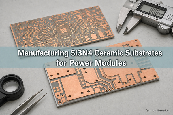
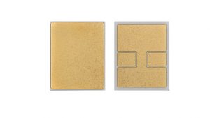
Manufacturing Si3N4 ceramic substrates for power modules, technical illustration

The Si3N4 chemical name is silicon nitride. In a silicon nitride ceramic substrate, the ceramic provides insulation while the metal layers form the circuit. Silicon carbide, or SiC, is different: a SiC semiconductor die can be mounted above a silicon nitride substrate, with each material performing a different job.

Why Do Thermally Cycled Power Modules Use Si3N4?

Power devices heat up under load and cool when the load falls. Copper and ceramic expand by different amounts, loading their bonded interface during each cycle. Si3N4 ceramic is attractive here because its resistance to crack propagation can support demanding copper-ceramic designs while retaining electrical insulation and a useful heat path.

This is why we consider the mechanical properties of silicon nitride alongside thermal performance. High silicon nitride thermal conductivity alone does not describe how a metallized substrate responds to copper thickness, edge defects or repeated temperature swings. The following Si3N4 material properties illustrate the different inputs to that decision.

Design input Electronic-substrate grade example Question it helps answer
Si3N4 thermal conductivity 85 W/m·K at 25°C How much thermal resistance does the ceramic thickness add?
Fracture toughness and bending strength 6.5 MPa·√m, indentation-fracture method; 800 MPa, three-point bending How does the selected grade resist crack growth and bending?
Si3N4 thermal expansion coefficient 2.6 ppm/K over 40–400°C What expansion mismatch must the copper-ceramic structure accommodate?
Si3N4 Young’s modulus 310 GPa How stiff is the ceramic in the mechanical model?

These are reference values for one commercial grade, not our finished-board acceptance limits. Use the selected grade’s silicon nitride coefficient of thermal expansion over the relevant temperature interval; a room-temperature value cannot describe an entire operating cycle.

Si3N4 properties make the material a strong candidate when mechanical reliability and heat removal must be addressed together. An AlN substrate may still be preferable where reducing ceramic-layer thermal resistance dominates the design, while alumina can suit less demanding, cost-sensitive circuits. The choice should follow the module’s loading and cooling requirements rather than a universal material ranking.

Building the Copper-Ceramic Structure with AMB

For a thick-copper power circuit, our AMB ceramic PCBs provide a manufacturing route that joins copper to the ceramic through active metal brazing. A Si3N4 AMB substrate combines current-carrying copper regions with an insulating ceramic core; the brazed interface connects the materials mechanically and thermally.

  1. Define the stack. We review the silicon nitride Si3N4 plate, copper on each face, finished dimensions and assembly surfaces against the circuit drawing.
  2. Join copper to ceramic. An active brazing material enables the metal-ceramic bond. This is a metallurgical joining layer, not an adhesive film.
  3. Form the isolated circuit regions. Patterning must define both the copper geometry and the required electrically isolated spaces. Conductive residues between islands cannot remain as unintended current paths.
  4. Finish the connection surfaces. We match the specified finish and pad condition to the subsequent attachment process before the circuit enters module assembly.

The copper thickness and isolation geometry must be developed together. Etching a thick conductor produces a sidewall profile, so the gap visible at the copper surface is not necessarily the same as the metal-free distance at the ceramic interface. We review the finished geometry, not only the artwork line.
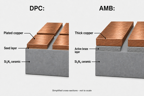
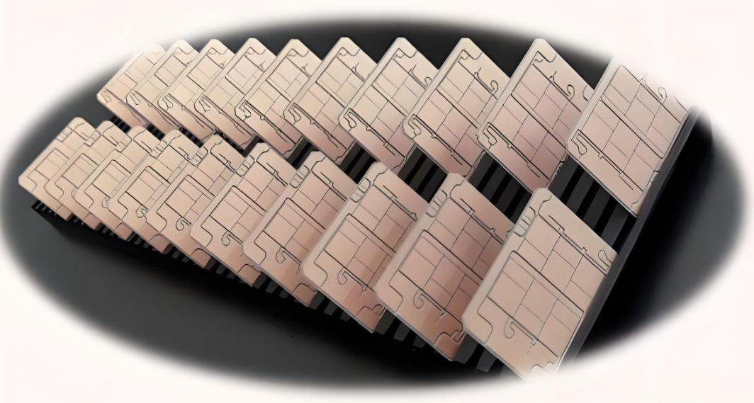
Simplified DPC and AMB Si3N4 ceramic circuit cross-sections with isolated copper patterns

Choosing DPC for Finer Si3N4 Circuit Geometry

Not every silicon nitride circuit needs thick brazed copper. If the design requires finer conductor geometry or thinner controlled metallization, our DPC ceramic PCBs offer another route. Direct plated copper uses deposited metallization and copper plating to create patterned tracks and pads on the ceramic.

A smaller feature capability is useful when connection density drives the layout, but it does not make DPC an automatic substitute for an AMB substrate carrying a different current or heat load. We select the route against the conductor structure and attachment requirements before applying the dimensional limits below.

Our Si3N4 Substrate Manufacturing and Customization Capabilities

We manufacture custom Si3N4 ceramic circuits with the copper layout, board outline and connection surfaces specified for the project. The following DPC and AMB process capabilities establish a starting point for engineering review; they are not a promise that every maximum and minimum can be combined on the same board.

Item Our DPC process Our AMB process
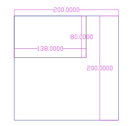
Maximum panel size 138 × 190 mm 114 × 114 mm
Copper thickness 2–200 µm 8–22.9 oz, about 0.28–0.80 mm
Minimum line / space 6 / 8 mil, about 0.15 / 0.20 mm 20 / 20 mil, about 0.50 / 0.50 mm
Circuit layers Two-layer capability Two-layer capability
Surface finish options OSP, ENIG, immersion silver OSP, ENIG, immersion silver

Customization covers the conductor pattern, pad locations, outline, hole positions and specified finish. We confirm ceramic grade and thickness with the copper construction rather than applying a generic ceramic thickness list to every Si3N4 build. Panel dimensions also include manufacturing margins; they are not the usable circuit area.

Design Details We Review Before Circuit Fabrication

A manufacturable substrate drawing describes more than an outline and a copper thickness. Our custom ceramic PCB manufacturing review connects the circuit artwork to the joining process, mechanical support and electrical isolation requirements.

Drawing or assembly input Our manufacturing review Why it matters
Copper islands, line spacing and thickness Review patterning allowance, pad shape and the required isolation after metal removal Heavy copper changes achievable geometry; narrow gaps require more than a nominal artwork dimension
Ceramic outline, holes and registration references Check the mechanical drawing against the copper artwork and assembly datums The circuit must align with the device placement, terminals and module mounting arrangement
Working voltage, ceramic thickness and conductor separation Define insulation test conditions and review clearance and creepage with the module design A material breakdown number is not the assembled module’s working-voltage rating

Material Data Needed Beyond the Copper Drawing

For electrical modeling, Si3N4 permittivity is grade- and frequency-dependent; an electronic-substrate example is 7.8 at 1 MHz. The electrical conductivity of silicon nitride is low in its insulating substrate form, so current should follow the copper rather than pass through the ceramic. Parasitic capacitance across that ceramic still matters in a fast-switching module.

Si3N4 density and Si3N4 hardness serve different manufacturing purposes: a grade example lists 3.22 g/cm³ and 15 GPa Vickers hardness. Density contributes to mass estimates; hardness informs machining considerations. Neither replaces fracture-toughness or edge-quality requirements when assessing a thin circuit plate.

Controlling Warpage and Edge Stress in Thick-Copper Si3N4 Substrates

Warpage control starts with the copper-ceramic construction, not just a flatness check at shipment. Copper on the two faces can differ in thickness, coverage and pattern position. Those differences, together with ceramic thickness and substrate dimensions, affect how the part bends as the bonded structure changes temperature.

During layout review, we examine the relationship between the front and back copper patterns, large copper islands, ceramic borders and assembly support points. Symmetry can help, but forcing identical copper on both faces may conflict with the electrical design. An asymmetric stack needs its own assessment rather than a universal rule that one copper ratio guarantees flatness.

At the perimeter, copper geometry, the metal-free ceramic border and existing edge defects influence local loading. Thick copper should not simply be extended to the ceramic edge to gain conductor area. We agree the relevant clearances and edge-acceptance criteria for the selected stack.

For a demanding mounting interface, the drawing should define the flatness measurement area and support condition. Initial samples can then be checked against the intended attachment surface before the construction is released for production. Substrate bow should not be corrected by forcing a brittle ceramic plate flat with excessive clamping load.

Selecting Surface Finishes for Die Attach and Interconnection

Surface finish selection must follow the assembly method. The same Si3N4 circuit can have die-attachment pads, wire-bond areas and an underside thermal interface, each with different requirements. A coating name alone does not specify a bondable or sinterable surface.

  • Soldered attachment: match the surface condition to the solder and flux system, storage controls and planned thermal exposures. Oxidation or contamination can undermine wetting even when the nominal finish is correct.
  • Wire bonding: identify the wire material and bonding process, then specify compatible pad metallurgy, cleanliness and roughness. A finish qualified for soldering is not automatically qualified for wire bonding.
  • Silver-sintered attachment: where the module design uses this method, confirm the paste’s required substrate and die-backside metallization. An immersion-silver option does not by itself establish a qualified sintering process.

We use the attachment specification to review the circuit’s finish requirements and achievable surface condition. The module assembler must validate the joining process on that surface. This keeps substrate fabrication and assembly qualification connected without implying that every finish or assembly process is interchangeable.

Matching the Substrate to the Module and Cooling Stack

In the finished assembly, heat travels from the semiconductor through its attachment layer, the upper copper, the ceramic and the lower interface toward a baseplate or cooler. The ceramic contributes only one part of that path. For a simplified uniform layer, its thermal resistance is R = t / (k × A), where t is thickness, k is thermal conductivity and A is heat-transfer area.
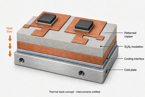
Si3N4 power-module thermal stack concept with semiconductor dies and cooling interface

Traction-Inverter Power Stages

Repeated acceleration and changing load create thermal excursions in the power stage. A Si3N4-based structure can address the combination of copper loading and ceramic crack resistance. For the circuit build, we need the device-pad layout, copper thickness, substrate attachment method and operating temperature range; the module design must also account for interconnect and joint fatigue.

Charger and Industrial-Drive Power Stages

In a charger’s switching bridge or an industrial drive’s power module, sustained losses and switching transients place demands on both heat removal and insulation. Substrate dimensions, conductor separation and the underside mounting surface therefore need to be developed with the cooling and packaging arrangement. Choosing a thinner ceramic solely to reduce thermal resistance can change insulation and mechanical margins.

These are application design scenarios for the circuit substrate, not claims that we manufacture complete traction inverters, chargers or motor drives. The illustration shows the heat-path concept; it is not a customer module or a production photograph.

Circuit Acceptance and Module-Level Validation

As a silicon nitride substrate manufacturer, we work with you to define acceptance requirements for the fabricated circuit. The inspection plan should address conductor geometry, continuity and isolation, ceramic edge condition, finished dimensions, flatness and surface condition. Joining-interface inspection requirements and suitable methods should be agreed for the selected process.
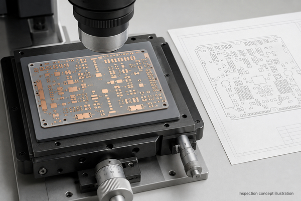
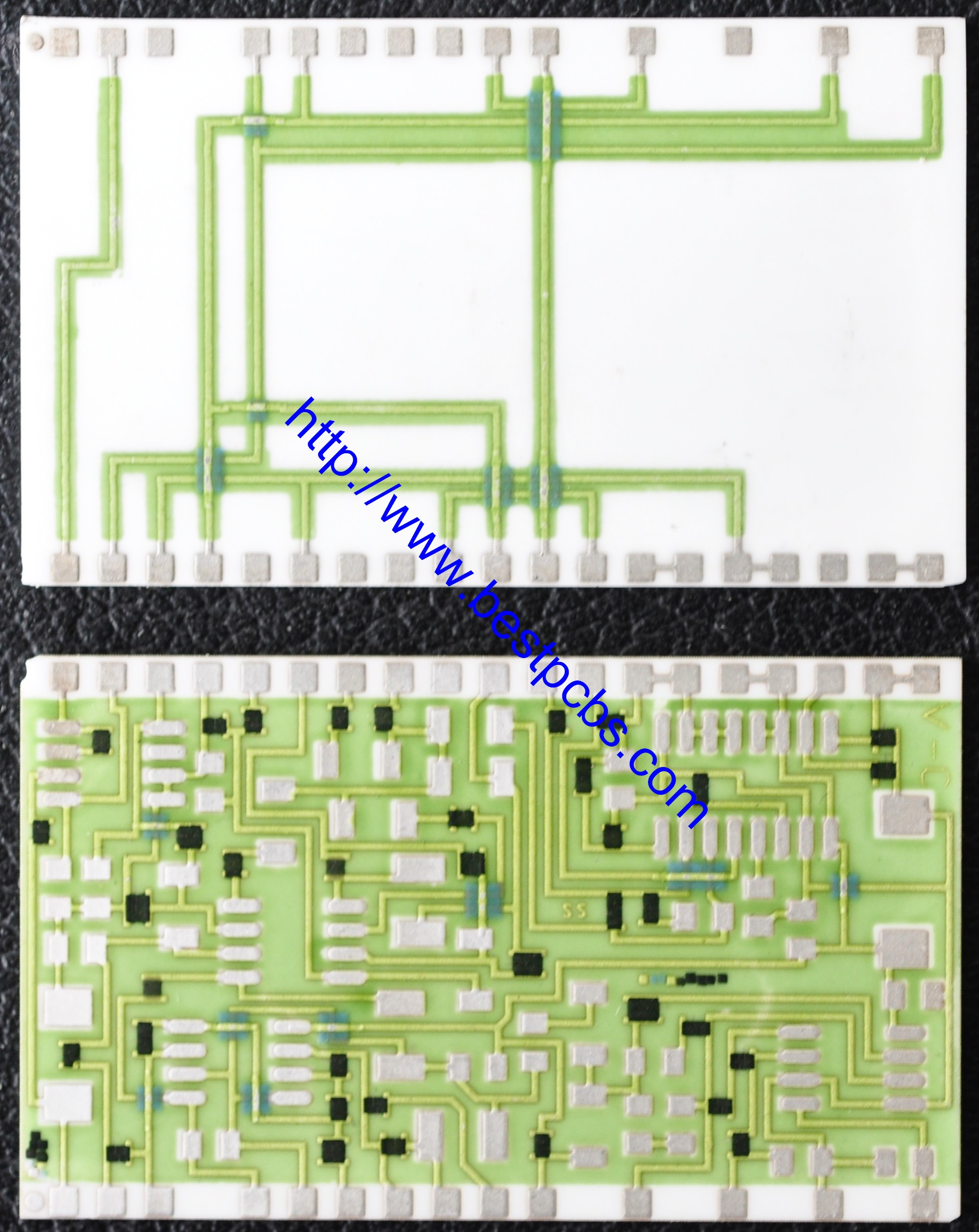
Optical inspection concept for a patterned Si3N4 ceramic circuit substrate

A circuit inspection and a module qualification answer different questions. The first checks whether the substrate meets its drawing and acceptance criteria. Thermal or power cycling, partial-discharge testing where required, and assembled thermal-performance validation establish behavior under the module’s actual operating conditions. An optical image cannot demonstrate those lifetime results.

When comparing silicon nitride manufacturers, distinguish bare-material specifications from the ability to manufacture the required copper circuit. Our role is ceramic circuit fabrication, with DPC or AMB process selection, manufacturability review and project-specific acceptance planning. We do not describe a raw-material datasheet as our own finished-module performance guarantee.

Si3N4 cost depends on material grade, dimensions, copper structure, finish and quantity. We review these together so the quoted construction matches the drawing. Send your circuit artwork, stack-up, attachment requirements and target quantity to sales@bestpcbs.com; our team can review a manufacturable Si3N4 configuration for your power-electronics project.
You may also like

AMB Ceramic PCB
Wednesday, April 1st, 2026

AMB Ceramic PCB is a high-performance ceramic substrate designed for power electronics that demand strong copper-to-ceramic bonding, efficient heat dissipation, and long-term reliability. At Best Technology, we provide custom AMB ceramic PCB solutions using Al2O3, AlN, and Si3N4 ceramic materials for customers in automotive, industrial, energy, rail transit, and high-power semiconductor industries.

If your project requires a substrate that can handle high current, thermal cycling, and harsh operating conditions, AMB PCB is a dependable choice.

Why Choose Best Technology for AMB Ceramic PCB?

At Best Technology (EBest Circuit), we provide advanced ceramic PCB solutions tailored for high-performance applications.

Our Strengths

  • 20+ years of PCB and PCBA experience
  • Support for Al2O3, AlN, and Si3N4 substrates
  • Copper thickness up to 800 µm
  • Strong expertise in power modules and thermal design
  • Full turnkey service from PCB to assembly
  • Certified with ISO 9001, ISO 13485, and IATF 16949

We work closely with engineers to optimize designs for manufacturability, reliability, and cost efficiency.

AMB Ceramic PCB

What Is AMB Ceramic PCB?

AMB stands for Active Metal Brazing. It is a ceramic substrate technology that bonds copper foil to ceramic by using active brazing materials containing metal elements such as titanium, silver, zirconium, or copper.

Unlike standard bonding methods, AMB creates a strong chemical bond between metal and ceramic at high temperature. This gives the finished substrate:

  • Higher bonding strength
  • Better resistance to thermal stress
  • Excellent heat transfer performance
  • Higher reliability in demanding environments

AMB ceramic PCB is widely used in power modules, IGBT modules, SiC packaging, EV systems, traction inverters, and renewable energy equipment.

Why Choose AMB Ceramic PCB?

For many power electronics projects, the substrate must do more than just carry traces. It must also help control heat, maintain insulation, and survive repeated thermal cycling. AMB ceramic PCB is chosen because it offers:

  • Stronger Bonding Performance

The active metal brazing process creates a reliable bond between copper and ceramic, making the substrate more suitable for high-power module packaging.

  • Better Reliability Under Thermal Stress

AMB substrates are designed for applications with frequent temperature changes and high operating loads. In advanced module structures, they can support very high thermal shock resistance.

  • Excellent Heat Dissipation

With the right ceramic material, AMB PCB can provide strong thermal performance for power semiconductors, converters, and high-current designs.

  • Good Match for Advanced Power Devices

AMB substrates are widely used with SiC chips, silver sintering processes, and thick copper designs, where both heat and reliability matter.

AMB Ceramic PCB vs DBC Ceramic PCB

Both AMB and DBC are used in ceramic substrate manufacturing, but they are not the same.

ItemDBC Ceramic PCBAMB Ceramic PCB
Bonding methodDirect bonding of copper to ceramicActive metal brazing
Process structureSimplerMore complex
Bonding strengthGoodHigher in many demanding applications
Thermal cycling reliabilityGoodExcellent
Suitable for harsh environmentsYesBetter suited for severe conditions
Typical high-reliability useStandard power modulesEV, traction, SiC, high-reliability power modules

In short, DBC is a strong option for many standard power applications, while AMB is often preferred when stronger bonding and better long-term reliability are required.

Ceramic Materials Available for AMB PCB

We provide AMB ceramic substrates based on different ceramic materials to match different power levels, cost targets, and reliability requirements.

1. Alumina AMB Ceramic PCB

Alumina is the most mature and cost-effective option.

Advantages:

  • Lower material cost
  • Stable supply
  • Mature manufacturing route
  • Good electrical insulation

Best for:

  • Cost-sensitive projects
  • Medium-power applications
  • Products with moderate thermal requirements

2. Aluminum Nitride AMB Ceramic PCB

AlN offers very high thermal conductivity, making it ideal for fast heat transfer.

Advantages:

  • High thermal conductivity
  • Excellent heat spreading
  • Suitable for high-power devices

Best for:

  • High-current applications
  • Power conversion systems
  • Compact designs with high heat density

3. Silicon Nitride AMB Ceramic PCB

Si3N4 is the preferred material for projects that require both mechanical reliability and thermal performance.

Advantages:

  • High bending strength
  • Strong thermal shock resistance
  • Thermal expansion closer to silicon
  • Excellent reliability in demanding environments

Best for:

  • Automotive power modules
  • Traction systems
  • Wind power converters
  • High-reliability SiC and IGBT packaging

Material Property Comparison

ItemUnitAl2O3AlNSi3N4
Densityg/cm³3.73.33.22
Thermal conductivityW/(m·K)>20>170>80
Coefficient of thermal expansionppm/°C6.94.72.5
Bending strengthMPa>350>350>700
Dielectric constant@1MHz9.89.08.0
Breakdown strengthkV/mm>15>20>20

Alumina AMB Ceramic PCB

Alumina ceramic PCB is the most mature and cost-effective option among AMB substrate materials.

Because alumina is widely available and easier to process, it is often used where budget control matters. The manufacturing base for alumina is also more established, which helps keep cost lower.

Advantages of Alumina AMB Substrates

  • Mature production process
  • Lower material cost
  • Stable electrical insulation
  • Good availability for volume production

Limitations of Alumina

The main limitation is its relatively low thermal conductivity. Compared with AlN and Si3N4, alumina transfers heat less efficiently. For that reason, it is more suitable for:

  • Low to medium power applications
  • Products with lower thermal load
  • Systems with moderate reliability requirements

Aluminum Nitride AMB Ceramic PCB

Aluminum nitride ceramic PCB is known for its very high thermal conductivity. This makes it a strong option for electronic products that need fast heat removal. With thermal conductivity above 170 W/(m·K), AlN performs much better than alumina in heat dissipation. It is often selected for:

  • High-power electronic devices
  • High-current modules
  • Power conversion systems
  • Applications with limited space for heat spreading

Benefits of AlN AMB Substrates

  • Excellent thermal conductivity
  • Strong electrical insulation
  • Good performance in high-power designs
  • Better thermal management than alumina

Design Consideration

Although AlN performs very well thermally, its mechanical toughness is not as strong as silicon nitride. In repeated high and low temperature cycling, this can limit its service life in some harsh environments.

So while AlN is a very capable choice, it is usually best for applications where heat transfer is the top priority, but extreme mechanical shock resistance is not the main concern.

Aluminum Nitride AMB Ceramic PCB

Silicon Nitride AMB Ceramic PCB

Silicon nitride ceramic PCB is often considered the premium choice for AMB applications that require both thermal performance and mechanical reliability.

Silicon nitride has a thermal conductivity above 90 W/(m·K) and a coefficient of thermal expansion very close to silicon. This helps reduce stress between the substrate and semiconductor chip during temperature changes.

It also offers very high bending strength, often above 700 MPa, which is much higher than alumina and AlN.

Why Si3N4 Stands Out

  • High mechanical strength
  • Good thermal conductivity
  • Excellent thermal shock resistance
  • Strong resistance to corrosion and oxidation
  • Better long-term reliability in harsh environments

High thermal conductivity silicon nitride ceramics usually contain a large proportion of the stable β-Si3N4 phase, which contributes to stronger and more reliable performance.

Typical Applications of Si3N4 AMB PCB

  • Automotive power modules
  • Wind turbine converters
  • Traction systems
  • High-voltage DC transmission
  • Power modules with partial discharge resistance requirements

In many advanced power systems, Si3N4 AMB substrates are selected when reliability matters just as much as heat dissipation.

Main Manufacturing Process of AMB Ceramic PCB

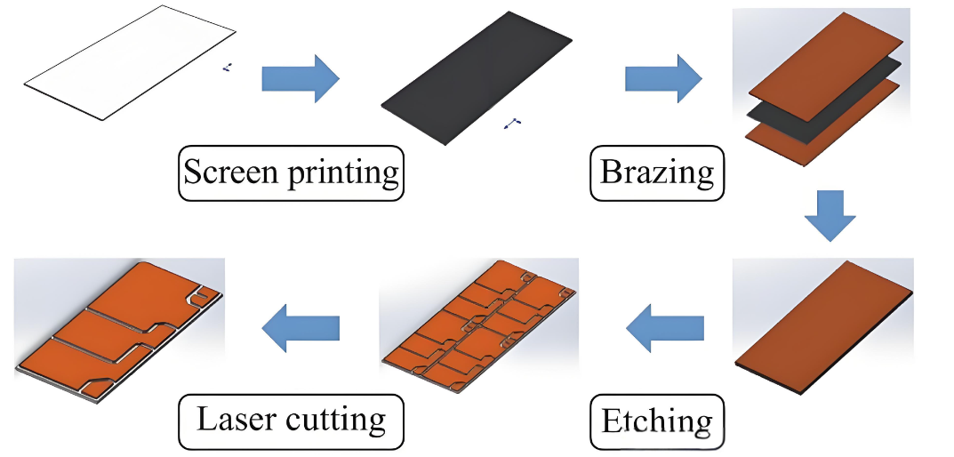
The manufacturing process of AMB ceramic PCB is more complex than standard PCB production because it combines ceramic processing, metal brazing, and precision patterning.

A typical AMB PCB production flow includes the following steps:

Main Manufacturing Process of AMB Ceramic PCB

1. Ceramic substrate preparation

The ceramic sheet is cleaned and prepared for bonding.

2. Active metal brazing paste or filler application

A brazing material containing active metal elements is applied evenly to the ceramic surface.

3. Copper foil alignment

Copper foil is placed on the ceramic substrate.

4. High-temperature brazing

The assembly is heated under controlled conditions so the active metal reacts with the ceramic and forms a strong bond.

5. Cooling and bond stabilization

The bonded structure is cooled carefully to maintain flatness and bond quality.

6. Circuit pattern imaging

The copper layer is patterned according to the circuit design.

7. Etching

Copper is etched, and in AMB structures the extra solder layer may also need to be removed.

8. Surface finishing and inspection

The finished substrate goes through surface treatment, dimensional inspection, and reliability checks.

Because AMB products include an additional brazing layer, the production route is more demanding than DBC. However, this extra process is also what enables AMB to achieve stronger bonding and better reliability in many power module applications.

Main Features of AMB PCB

  • High bonding strength between copper and ceramic
  • Excellent thermal dissipation for high-power devices
  • Strong thermal cycling reliability
  • Good compatibility with SiC and other advanced semiconductors
  • Stable electrical insulation under demanding conditions
  • High mechanical durability, especially with silicon nitride
  • Support for thick copper layers, in some cases up to 800 μm
  • Suitable for high-voltage and high-current applications

Common Applications of AMB Ceramic PCB

  • High-power semiconductor modules
  • High-frequency switching devices
  • Wind power systems
  • Solar energy equipment
  • Automotive electronics
  • Locomotives and rail transportation
  • Aerospace electronics
  • IGBT modules
  • 5G communication electronics
  • Medical devices
  • High-power LED lighting
  • Industrial control equipment
  • Defense and security systems

These applications often require a substrate that can operate under heat, vibration, current stress, and repeated thermal cycling without early failure.

Need a Reliable AMB Ceramic PCB Supplier?

If you are looking for an AMB ceramic PCB manufacturer for automotive, IGBT, SiC, renewable energy, or industrial power applications, Best Technology is ready to support your project.

Send us your design files or technical requirements, and our engineering team will review them and provide a suitable solution.

Email: sales@bestpcbs.com

You may also like

AMB Ceramic PCB | Ceramic PCB Prototype & Design
Thursday, October 17th, 2024

What is Active Metal Brazing (AMB) Technology?

AMB technology is developed on the basis of DBC technology, at a high temperature of about 800 ° C, AgCu solder containing active elements Ti and Zr is wetted and reacted at the interface of ceramics and metals, so as to achieve heterogeneous bonding between ceramics and metals.

Compared with traditional products, AMB ceramic PCB relies on the chemical reaction of ceramic and active metal solder paste at high temperature to achieve the combination, so its combination strength is higher, better reliability, extremely suitable for connectors or scenarios with large current load and high heat dissipation requirements. In particular, new energy vehicles, rail transit, wind power generation, photovoltaic, 5G communication and other power electronics and high-power electronic modules with demanding performance requirements have a huge demand for AMB ceramic copper clad plates. At present, this kind of product is becoming one of the mainstream products in the market.

AMB Ceramic PCB | Ceramic PCB Prototype & Design

Why use AMB Ceramic PCB?

The main benefits of AMB ceramic substrates include excellent thermal conductivity, copper layer bonding, reliability and suitability for high power and current applications. ‌ AMB ceramic substrate compared with the traditional DBC ceramic substrate, in the thermal conductivity, copper layer bonding force, reliability and other aspects of better performance, especially suitable for high temperature, high power, high heat, high reliability package requirements.

Specifically, the AMB ceramic substrate is welded between the copper foil and the ceramic substrate using a metal solder containing a small amount of active elements. This process improves the wettability of the solder to the ceramic after melting, so that the ceramic surface can be welded with the metal without metallization, thereby improving the thermal conductivity and copper layer bonding force.

In addition, the characteristics of AMB ceramic substrate with high current carrying capacity and low thermal expansion coefficient make it excellent in IGBT module, vehicle gauge main inverter, photovoltaic transformer, rail transit high voltage and other application.

What is the difference between DBC and AMB ceramic PCB?

Both DBC and AMB technologies use ceramic as the base material, but their bonding processes are different, leading to distinct performance characteristics.

  • Bonding Process: DBC relies on a high-temperature process to bond copper directly onto a ceramic substrate. AMB, on the other hand, uses active metal brazing, where metals like titanium and zirconium are added to form a strong bond between the copper and ceramic.
  • Thermal Conductivity: AMB ceramic PCBs are known for better thermal conductivity compared to DBC.
  • Mechanical Strength: AMB ceramic PCBs typically offer superior mechanical strength due to the brazing process. The bond is more durable and reliable under extreme conditions.
  • Flexibility in Design: AMB technology allows for more flexibility in terms of the shapes and sizes of copper patterns, which can be a big advantage in custom designs. DBC, while effective, can sometimes be limited in this regard.

AMB Ceramic PCB Manufacturing Process

The process of creating AMB ceramic PCBs is intricate and requires precision at every step. Here’s an overview of the key stages involved:

1. Ceramic Substrate Preparation: The first step is choosing the right ceramic substrate. Common materials include aluminum nitride and alumina, both known for their excellent thermal properties.

2. Metal Deposition: Copper is the most common metal used for AMB ceramic PCBs. However, unlike traditional methods, an active metal like titanium or zirconium is added to the copper to form a strong bond with the ceramic substrate.

3. Active Metal Brazing: The ceramic and metal are heated to a high temperature, allowing the active metals to react with both the copper and ceramic. This process forms a bond that is stronger than conventional methods like soldering or adhesion.

4. Etching and Circuit Formation: Once the copper has bonded with the ceramic, the next step is to etch the copper to create the desired circuit patterns. This is done using precise laser technology to ensure high accuracy.

5. Inspection and Testing: Quality control is vital in AMB ceramic PCB manufacturing. Each PCB is carefully inspected for defects and tested to ensure it meets the necessary performance criteria.

Types of Ceramic Substrate

Nowadays, there are four common types of ceramic substrates used in the ceramic PCB manufacturing – Al2O3, AlN, BeO and Si3N4. Let me introduce them firstly:

1. Al2O3

    Al2O3 (Alumina) substrate is the most commonly used substrate material in the electronics industry. Compared with most other oxide ceramics, alumina ceramics have high strength and chemical stability, rich raw material sources, cheap prices, and are suitable for a variety of manufacturing technologies and different shape requirements.

    2. BeO

    BeO has a higher thermal conductivity than metal aluminum, applied to the need for high thermal conductivity, but the temperature exceeds 300°C rapidly decreases, but also due to its toxicity, greatly limiting the application of BeO ceramics.

    3. Si3N4

    The thermal conductivity of silicon nitride ceramic substrate 75-80W/(m·K), the thermal conductivity is indeed less than that of aluminum nitride ceramic substrate, but the bending strength of silicon nitride ceramic substrate is 2-3 times that of aluminum nitride ceramic substrate, which can improve the strength and impact resistance of silicon nitride ceramic copper-clad plate, welding thicker oxygen free copper without porcelain cracking phenomenon, and improve the reliability of the substrate.

    4. AlN

    AlN has several very important performance advantages: it is non-toxic; High insulation performance and high breakdown field strength (1.4×10⁷V/cm); Low dielectric constant (~ 8.8); Very high thermal conductivity (comparable to good thermal conductivity of aluminum, theoretical thermal conductivity 280W/m/K); There is an expansion coefficient matching Si (293K-773K, 4.8×10⁻⁶K-1). Only the mechanical strength of AlN ceramic material itself is slightly worse; Compared with Al2O3, the price of AlN is relatively high. However, in terms of cost performance, AlN is still much higher, because the thermal conductivity of Al2O3 (96%) is only 29W/M*K (25°C), and the thermal conductivity of AlN is as high as 180W/M*K (25°C). Therefore, for the emerging and rapidly developing high-power electronic devices required by the Internet of Things, artificial intelligence, 5G, power electronics, rail transit, new energy vehicles and other industries, especially high-power IGBT modules, aluminum nitride ceramic substrates with high thermal conductivity and high reliability will become the preferred material.

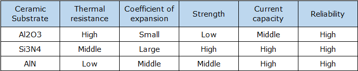
    Among them, only Al2O3, AlN and Si3N4 can be MADE by AMB technology. Below is a performance table of AMB ceramic PCB made with different materials:

    AMB Ceramic PCB | Ceramic PCB Prototype & Design

    How Much Does an AMB PCB Cost?

    The cost of an AMB ceramic PCB depends on several factors, each influencing the overall price.

    • Material Choice

    The type of ceramic used plays a significant role in the cost. Aluminum nitride is more expensive than alumina but offers superior thermal properties. Depending on the application, choosing the right material is key to balancing cost and performance.

    • Copper Thickness

    Thicker copper layers increase the price due to the additional material required. However, they also improve the current-carrying capacity, which might be necessary for high-power devices.

    • Design Complexity

    More intricate designs, especially those with custom shapes or numerous layers, will naturally cost more due to the precision required during manufacturing.

    • Batch Size

    Ordering AMB ceramic PCBs in bulk can reduce the cost per unit. This is particularly beneficial for larger companies that require high-volume production.

    • Testing and Quality Assurance

    Rigorous testing and quality checks are essential for AMB ceramic PCBs, especially in industries where failure is not an option. Higher standards of quality control can drive up costs but ensure greater reliability.

    Challenges Facing AMB Technology

    While AMB technology offers numerous advantages, it is not without its challenges. Understanding these challenges is crucial for its successful implementation in ceramic circuit boards.

    1. Cost Considerations

    One significant hurdle to the widespread adoption of AMB technology is cost. The materials involved in AMB, particularly the reactive filler metals, can be more expensive than traditional bonding methods. Additionally, the equipment and processes required for AMB may involve higher initial investments.

    2. Process Complexity

    The AMB process demands a high degree of precision and control. Factors such as temperature, environment, and timing must be meticulously managed to ensure optimal bonding quality.

    3. Limited Availability of Filler Materials

    The selection of suitable filler materials for AMB can be restrictive. Finding a filler that effectively bonds with various ceramics and metals while maintaining desirable mechanical and thermal properties can be a daunting task.

    4. Risk of Thermal Shock

    The high temperatures associated with the AMB process pose a risk of thermal shock to the ceramic substrates. If not properly managed, rapid temperature changes can lead to cracking or other failures in the ceramic material. Careful consideration of thermal profiles during the brazing process is essential to mitigate this risk.

    EBest Circuit (Best Technology) is a reliable Ceramic PCB manufacturer in China. We specialize in small to medium-volume PCB Manufacture, PCB Assembly and Electronic Manufacturing Services. Our product ranges from thick film ceramic PCB, thin film ceramic PCB, DPC ceramic PCB, DBC ceramic PCB, AMB ceramic PCB, HTCC ceramic PCB and LTCC ceramic PCB. Choose us, you can enjoy:

    • High Quality
    • Turn-key Service
    • Competitive Pricing
    • No MOQ & Fully Flexible
    • Certificated with ISO9001, ISO13485, IATF16949, UL
    • 99% On-time Delivery
    • One time design successfully
    • VIP sales assistant service
    • WIP online checking

    You may also like