

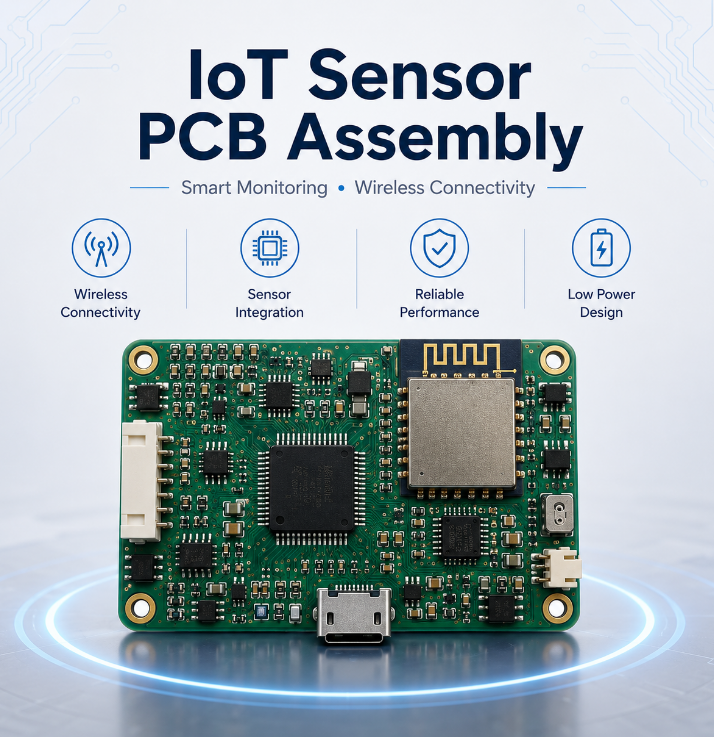
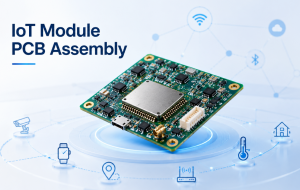
Looking for reliable IoT sensor PCB assembly for smart monitoring and wireless devices? A qualified IoT sensor PCBA must support accurate sensing, stable wireless transmission, low power consumption, and long-term field reliability. It is commonly used in smart buildings, industrial monitoring, asset tracking, agriculture, security devices, energy systems, and wearable electronics.
In real production, small assembly issues can quickly affect the whole device. Poor soldering, wrong sensor placement, weak RF control, unstable power supply, or missing test points may cause data errors, short battery life, weak signal, or delivery delays. This article explains the key components, assembly process, quality control, testing requirements, common problems, and supplier selection points for IoT sensor PCB assembly.
What Is IoT Sensor PCB Assembly?
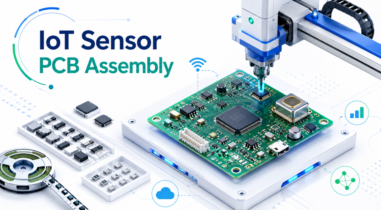
IoT sensor PCB assembly is the process of mounting and soldering sensors, wireless modules, MCUs, power circuits, connectors, and protection components onto a printed circuit board. After assembly, the board can collect data, process signals, transmit information, and work as the electronic core of a smart monitoring device.
Unlike standard PCB assembly, IoT sensor PCB assembly must consider sensor accuracy, RF performance, power consumption, firmware loading, and functional testing at the same time. A small error in sensor placement, antenna area, soldering quality, or power circuit control can affect data stability and wireless communication.
A complete IoT sensor PCBA project usually includes PCB fabrication, component sourcing, SMT assembly, through-hole assembly if required, inspection, programming, testing, and final packaging. For smart monitoring and wireless devices, the goal is not only to assemble components correctly, but also to make the board stable, testable, and ready for real application use.
Where Is IoT Sensor PCB Assembly Used in Smart Monitoring Devices?
IoT sensor PCB assembly is used in products that collect real-world data and send it to a gateway, cloud platform, mobile app, or control system. These products are common in smart buildings, industrial monitoring, logistics, agriculture, medical electronics, energy systems, and security devices.
Main application areas include:
- Smart buildings: air quality monitoring, occupancy detection, lighting control, HVAC monitoring
- Industrial monitoring: vibration monitoring, machine status detection, energy tracking
- Logistics: cold chain monitoring, GPS tracking, shock detection, humidity tracking
- Agriculture: soil monitoring, weather stations, irrigation control
- Security devices: motion detection, door sensors, smart alarms
- Medical and wearable devices: portable monitoring, body temperature, motion sensing
Each application has different requirements for sensor accuracy, wireless range, power consumption, board size, and environmental protection. Therefore, the assembly plan should match the final working environment before production starts.
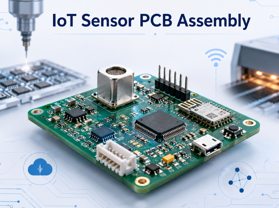
What Components Are Used in IoT Sensor PCB Assembly?
An IoT sensor PCBA usually combines sensing, control, communication, power, storage, connection, and protection circuits. Each part affects final device performance, so BOM accuracy and component quality should be reviewed before production.
| Category | Examples | Function |
|---|---|---|
| Sensor Unit | Temperature, humidity, vibration, gas, pressure | Data collection |
| MCU | STM32, ESP32, Nordic, NXP, TI | Signal processing |
| Wireless Module | Wi-Fi, BLE, LoRa, NB-IoT, LTE-M, Zigbee | Data transmission |
| Power Circuit | LDO, DC-DC, PMIC, charger IC | Voltage control |
| Memory | Flash, EEPROM | Data storage |
| Connector | USB-C, FPC, board-to-board, pin header | External connection |
| Protection | TVS, ESD diode, fuse, surge protector | Circuit safety |
Many IoT sensor boards use compact packages such as 0201, 0402, QFN, LGA, BGA, and fine-pitch ICs. Because of this, solder paste volume, SMT placement accuracy, and reflow profile control directly affect assembly quality.
Before batch production, component lifecycle and supply stability should also be reviewed. If a sensor IC, wireless module, or MCU has a long lead time, an approved alternative can help protect the production schedule.
Which Sensors Are Commonly Used in Smart Monitoring Devices?
Smart monitoring devices use different sensors according to the data they collect. The sensor choice depends on the application, working environment, accuracy level, power consumption, and enclosure structure.
Common sensor types include:
- Environmental sensors: temperature, humidity, air quality, CO2, PM2.5, VOC, light, pressure
- Industrial sensors: vibration, current, proximity, flow, tilt, magnetic, acceleration
- Security sensors: PIR motion sensor, reed switch, light sensor, sound sensor
- Wearable sensors: pressure, motion, body temperature, pulse-related sensing
- Agriculture sensors: soil moisture, pH, light, water level, outdoor temperature
Sensor placement must be handled carefully during IoT sensor PCB assembly. Heat sources, blocked airflow, vibration direction, RF circuits, and enclosure openings can all affect measurement accuracy.
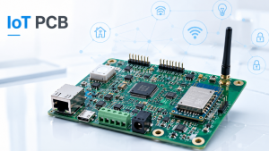
What Wireless Functions Should an IoT Sensor PCB Support?
Wireless function allows the IoT sensor board to send collected data to another device or platform. Common wireless options include Wi-Fi, BLE, LoRa, NB-IoT, LTE-M, Zigbee, Sub-GHz, and proprietary RF communication.
| Wireless Type | Common Use | Key Concern |
|---|---|---|
| Wi-Fi | Smart home, gateway devices | Higher power use |
| BLE | Wearables, short-range sensors | Battery life |
| LoRa | Outdoor and remote monitoring | Antenna tuning |
| NB-IoT / LTE-M | Asset tracking, smart meters | Peak current |
| Zigbee | Smart building systems | Network stability |
| Sub-GHz | Industrial and security devices | RF range |
For wireless IoT sensor PCB assembly, antenna clearance and RF layout are critical. The antenna area should avoid metal parts, batteries, screws, dense copper, and enclosure blockage.
Poor RF control can cause weak signal, unstable connection, higher retry rate, and shorter battery life. Therefore, wireless module placement, RF matching, shielding, and enclosure influence should be reviewed before production.
What Should Be Checked Before IoT Sensor PCB Assembly?
Before IoT sensor PCB assembly starts, production files and key requirements should be checked clearly. This helps reduce wrong parts, soldering errors, testing delays, and unstable device performance.
Key items to confirm include:
- Gerber files: PCB layers, drill files, solder mask, silkscreen, outline, and surface finish
- BOM: part number, package, value, tolerance, quantity, and replacement options
- Pick-and-place file: component position, rotation, polarity, and reference designator
- Assembly drawing: connector direction, special parts, manual soldering notes, and label position
- Sensor area: heat source distance, airflow path, exposure window, and mounting direction
- Wireless area: antenna keep-out, RF matching circuit, grounding, and enclosure influence
- Test points: power rails, programming port, communication interface, and sensor signals
For compact sensor boards, small file errors can cause major production problems. Polarity, footprint, antenna clearance, and test access should be checked before assembly begins.
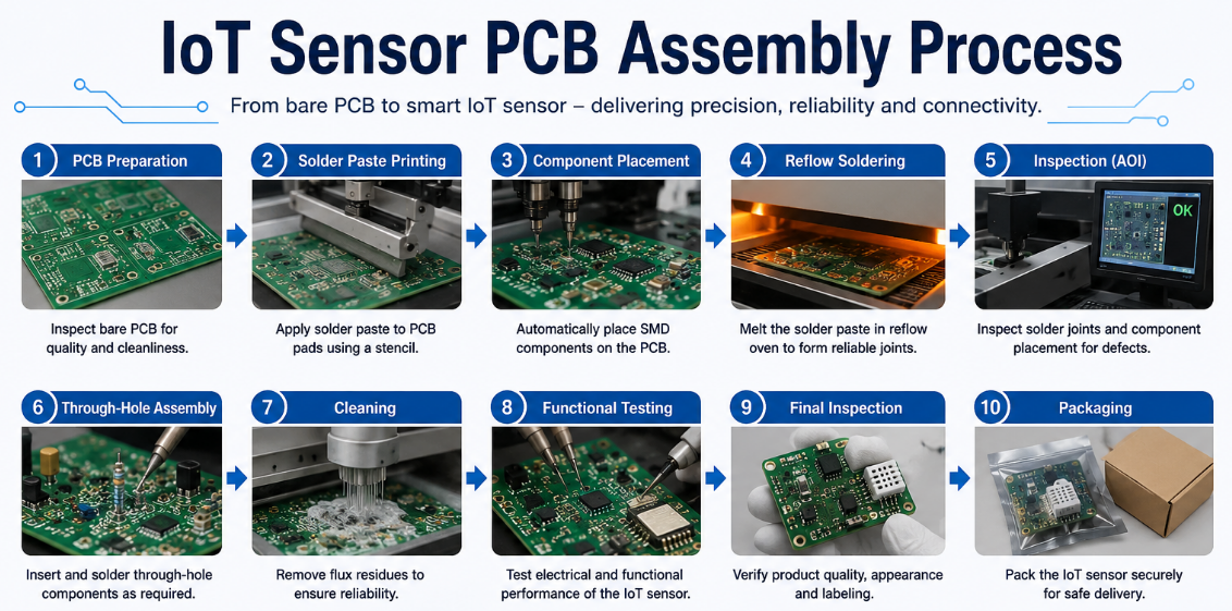
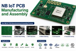
What Is the IoT Sensor PCB Assembly Process?
The IoT sensor PCB assembly process should be controlled from file review to final testing. Sensor boards often combine small components, wireless modules, low-power circuits, and sensitive sensor areas, so each step must be clear and traceable.
Step 1: Review files and BOM
Gerber files, BOM, pick-and-place files, and assembly drawings are checked before production. This step helps find wrong footprints, missing polarity marks, unavailable components, unclear connector directions, and possible soldering risks.
Step 2: Prepare PCB and components
The bare PCB is fabricated according to board thickness, surface finish, solder mask, and stack-up requirements. Components are checked by part number, package, quantity, moisture level, and storage condition before SMT production.
Step 3: Print solder paste
Solder paste is printed onto PCB pads through a stencil. For compact IoT sensor boards, paste volume and alignment must be controlled carefully because fine-pitch ICs and small passive parts are sensitive to excess or insufficient solder.
Step 4: Place SMT components
SMT machines place sensors, MCUs, wireless modules, power ICs, resistors, capacitors, and connectors onto the PCB. Accurate placement is important for 0201, 0402, QFN, LGA, BGA, and fine-pitch components.
Step 5: Complete reflow soldering
The board passes through a controlled reflow oven to form solder joints. A proper reflow profile helps reduce solder bridges, tombstoning, poor wetting, component shifting, and thermal damage to sensitive parts.
Step 6: Add secondary assembly
If the board includes through-hole connectors, terminals, battery holders, shield cans, or special mechanical parts, secondary assembly is arranged. This may include manual soldering, selective soldering, or fixture-assisted assembly.
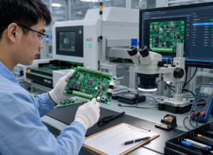
Step 7: Inspect, program, and test
After soldering, the board goes through AOI, visual inspection, X-ray if required, firmware loading, functional testing, wireless testing, sensor response checking, and final inspection before shipment.
What Quality Controls Are Needed During IoT Sensor PCB Assembly?
Quality control for IoT sensor PCB assembly should focus on soldering quality, component direction, RF area, sensor position, and powered performance. These are the areas most likely to affect final device reliability.
Incoming material inspection
PCBs and components should be checked before production. This includes part number, package, quantity, appearance, moisture status, and storage condition. This step helps avoid wrong parts, damaged components, and moisture-related soldering issues.
Solder paste inspection
SPI checks solder paste height, area, volume, and position before placement. This is useful for fine-pitch ICs, QFN packages, small passive components, and dense layouts where paste defects can quickly cause solder bridges or open joints.
SMT placement control
Placement control checks position, rotation, polarity, and package matching. Sensors, LEDs, diodes, ICs, wireless modules, and connectors must be mounted in the correct direction because one polarity error can cause board failure.
Reflow profile control
The reflow profile should match solder paste type, PCB thickness, component size, and thermal sensitivity. Good profile control improves solder joint consistency and reduces tombstoning, voids, poor wetting, and heat damage.
AOI and X-ray inspection
AOI checks visible defects such as missing parts, wrong polarity, offset parts, and solder bridges. X-ray is useful for QFN, BGA, LGA, and hidden solder joints where surface inspection cannot show the full solder condition.
Process traceability
For batch production, component lot records, inspection results, testing data, and production feedback should be traceable. This makes quality control clearer and helps locate the root cause quickly if an issue appears later.
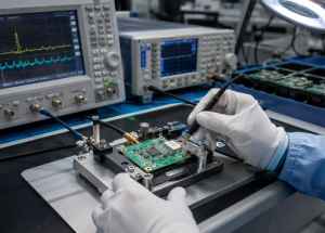
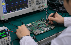
What Testing Is Required for IoT Sensor PCB Assembly?
Testing is important because many problems in IoT sensor PCB assembly only appear after the board is powered, programmed, and connected. A clear test plan helps verify sensor response, wireless communication, power stability, and product function.
Basic electrical test
Electrical testing checks shorts, opens, power rails, voltage output, resistance values, and current draw. It helps find solder bridges, wrong components, missing parts, and power circuit problems before full function testing.
Power consumption test
Many IoT sensor devices are battery-powered, so current should be measured in different states. Standby current, sleep current, wake-up current, peak current, and wireless transmission current can directly affect battery life.
Firmware loading test
Firmware loading confirms that the MCU or wireless module can be programmed correctly. Programming pads, boot mode, reset pin, communication interface, and flash memory should be checked during this step.
Sensor function test
Sensor testing verifies whether the board can collect correct data. Depending on the product, this may include temperature response, humidity response, pressure signal, motion detection, vibration response, gas output, or light sensing.
Wireless communication test
Wireless testing checks pairing, signal strength, transmission response, antenna performance, and connection stability. This is important for Wi-Fi, BLE, LoRa, NB-IoT, LTE-M, Zigbee, and Sub-GHz sensor boards.
Calibration test
Some sensors require calibration after assembly to improve accuracy. This is common for gas sensors, pressure sensors, humidity sensors, temperature sensors, and current sensors. Calibration standards and acceptance ranges should be clear before production.
Final functional test
Final testing should simulate basic product operation. It may include power-on test, data upload test, LED or button test, connector test, relay output test, wireless response test, and sensor reading verification.
What Common Problems Occur in IoT Sensor PCB Assembly Projects?
IoT sensor PCB assembly projects often face issues in sensor accuracy, wireless signal, power stability, soldering quality, firmware loading, and field reliability. These problems should be reviewed before batch production to reduce rework and delivery risk.
Unstable sensor data
Unstable data is often caused by poor grounding, heat interference, blocked airflow, wrong sensor direction, or nearby noisy circuits. Temperature sensors should stay away from heat sources, and gas or humidity sensors should have proper exposure to airflow.
Weak wireless signal
Weak signal may happen when the antenna area is blocked by copper, batteries, screws, metal housings, shield cans, or dense components. Antenna clearance, RF matching, module placement, and enclosure influence should be checked before production.
Short battery life
Battery-powered sensor devices may drain quickly if sleep current is high, the regulator is inefficient, or wireless transmission consumes too much current. Standby current, peak current, charger circuit, and wake-up timing should be tested.
Soldering defects
Fine-pitch ICs, QFN packages, small passive parts, and compact layouts can increase the risk of solder bridges, open joints, tombstoning, voids, and poor wetting. Stencil design, paste printing, placement accuracy, and reflow control help reduce these problems.
Sensor drift after assembly
Sensor drift can appear when the sensor is too close to heat-generating components, airflow is blocked, or calibration is missing. Proper placement and calibration help improve consistency for temperature, humidity, gas, pressure, and current sensors.
Programming or boot failure
Programming failure may come from wrong firmware, unstable power rails, poor contact with programming pads, missing boot mode control, or unclear test instructions. Clear programming files and stable test access make production testing more reliable.
Moisture and environmental damage
Boards used outdoors, in factories, warehouses, agriculture, or humid environments may face moisture, dust, vibration, and corrosion. Conformal coating, clean soldering, stronger connector control, and reliability testing can improve field performance.
How to Choose a Reliable IoT Sensor PCB Assembly Manufacturer?
A reliable IoT sensor PCB assembly manufacturer should control more than SMT placement. The right partner should understand sensors, wireless modules, low-power circuits, compact layouts, and testing requirements.
Check sensor assembly experience
The manufacturer should understand how sensor position affects data accuracy. Temperature sensors should stay away from heat sources, while humidity, gas, and air quality sensors should have proper exposure to airflow.
Confirm wireless module capability
For Wi-Fi, BLE, LoRa, NB-IoT, LTE-M, Zigbee, or Sub-GHz boards, the manufacturer should check antenna clearance, RF area, module placement, and enclosure influence before production.
Review SMT production ability
IoT sensor PCBAs often use 0201, 0402, QFN, LGA, BGA, fine-pitch ICs, and compact connectors. The manufacturer should support accurate solder paste printing, SMT placement, reflow control, AOI, and X-ray inspection when required.
Ask about BOM and sourcing review
A good manufacturer should check part numbers, package types, lead time, lifecycle status, and possible alternatives before assembly. This helps reduce wrong parts, material delays, and risky substitutions.
Confirm testing support
The manufacturer should support firmware loading, power rail checking, functional testing, wireless communication testing, current measurement, and sensor response testing according to project requirements.
Check prototype and batch support
Prototype assembly helps verify function and assembly feasibility. Batch production requires stable process control, repeatable testing, material consistency, and clear inspection records.
Evaluate communication quality
Choose a manufacturer that gives clear feedback on missing files, unclear drawings, risky components, missing test points, and assembly concerns. Clear feedback helps avoid delays and rework.
Prefer one-stop PCB and PCBA service
For IoT sensor PCB assembly projects, one-stop support for PCB fabrication, SMT assembly, sourcing, inspection, programming, and testing can reduce communication gaps and make production easier to control.
Why Choose EBest for IoT Sensor PCB Assembly Services?
EBest provides IoT sensor PCB assembly services for smart monitoring devices, wireless modules, industrial sensing products, smart home devices, tracking systems, and connected electronic products. Our service covers PCB fabrication, SMT assembly, component sourcing, inspection, testing, and production support.
One-stop PCB and PCBA support
EBest can support PCB fabrication, SMT assembly, component sourcing, through-hole assembly, inspection, and testing in one workflow. This helps reduce separate communication steps and makes project coordination more efficient.
Support for compact IoT sensor boards
Many IoT sensor boards use fine-pitch ICs, small passive components, wireless modules, shield cans, compact connectors, and sensitive sensors. EBest focuses on stable SMT placement, accurate soldering, controlled reflow profiles, and reliable inspection.
Practical review before assembly
Before production, EBest can review assembly risk, BOM availability, test points, wireless module placement, sensor position, and quality requirements. This helps reduce preventable production issues and improves batch consistency.
Testing support for connected devices
EBest can provide AOI inspection, X-ray inspection, firmware loading support, functional testing, wireless testing support, visual inspection, and packaging control according to project requirements. These steps help improve delivery reliability for smart monitoring and wireless devices.
Prototype to batch production support
EBest supports both prototype samples and batch production. Early samples help verify function and assembly feasibility, while batch production focuses on repeatable process control, stable quality, and reliable delivery.
FAQs About IoT Sensor PCB Assembly
Q1: Can I send only partial files first for an initial review?
A1: Yes. You can send available files first, such as Gerber files, BOM, or sample photos. For a formal quotation, Gerber, BOM, pick-and-place file, quantity, and testing notes will make the quote more accurate.
Q2: Can one project include several PCB revisions?
A2: Yes. If your project has different versions, mark each revision clearly in the file name and BOM. This helps avoid mixing old and new files during production.
Q3: Can assembled boards be packed for direct device integration?
A3: Yes. EBest can arrange anti-static bags, trays, labels, barcode stickers, moisture protection, and export packaging according to the project requirements.
Q4: Can EBest support repeat orders after the first batch?
A4: Yes. Repeat orders can be supported with saved production data, BOM records, process notes, and inspection requirements. This helps make later batches more consistent.
Q5: Can special labels or serial numbers be added?
A5: Yes. Labels, serial numbers, QR codes, and batch tracking marks can be added when the label format and location are provided before production.
Q6: Can EBest help with urgent project schedules?
A6: Yes. Urgent schedules can be reviewed based on PCB complexity, component availability, testing scope, and quantity. Clear files and confirmed components help speed up production planning.
Get a Fast Quote for Your IoT PCB Assembly Project
Ready to move your IoT PCB assembly project forward? Send your Gerber files, BOM, pick-and-place file, quantity, and special requirements to sales@bestpcbs.com. If your board includes sensors, wireless modules, firmware loading, coating, calibration, or custom packaging, include these details so we can prepare a more accurate quote.
EBest will review your project files and reply with practical production advice, clear cost information, and a suitable assembly plan. Whether your project is for smart monitoring devices, wireless sensor modules, industrial sensing products, or connected electronic boards, we can help you start production with fewer communication gaps and better quality control.
Share your project details now, and our team will help you confirm the next production step quickly and professionally.
You may also like

Tags: IoT Sensor PCB Assembly, IoT Sensor PCB Assembly Manufacturer, IoT Sensor PCB Assembly Services