PCB manufacturing PCB manufacturing
Home > Blog

PCB stencil

Precision Solder Paste Stencil for Reliable SMT PCB Assembly
Wednesday, June 24th, 2026

A solder paste stencil is one of the first process tools used in SMT PCB assembly, but it has a direct impact on final soldering quality. It controls solder paste volume, pad coverage, paste release, and solder joint consistency after reflow. A well-designed stencil helps reduce common SMT defects such as solder bridging, insufficient solder, tombstoning, solder balls, BGA open joints, and excessive voiding under exposed pads.

EBest Circuit supports SMT stencil and PCB assembly projects with laser-cut stencils, etched stencils, framed and frameless options, electro-polished apertures, fiducial marks, step-up/down technology, and BGA ball mounting stencils. Our team can review Gerber files, paste layers, BOM, Pick-and-Place files, and assembly requirements before production to help improve solder paste printing stability. For solder paste stencil support or full and partial turnkey PCB assembly, please send your files and requirements to sales@bestpcbs.com.

solder paste stencil

What Is a Solder Paste Stencil?

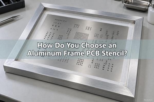
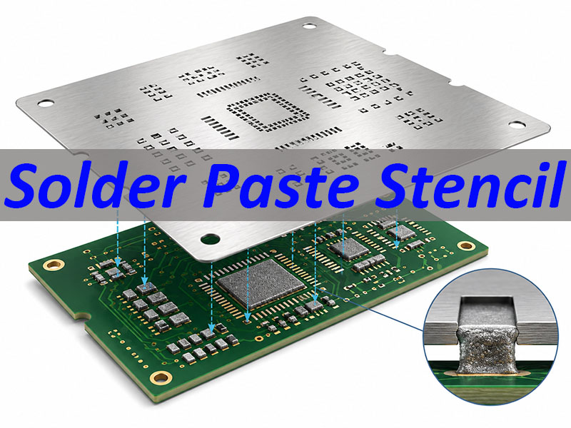
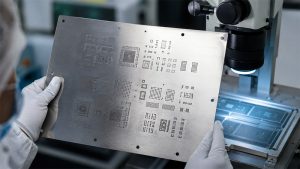
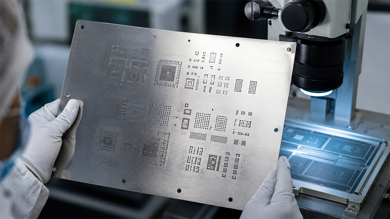
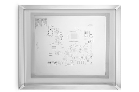
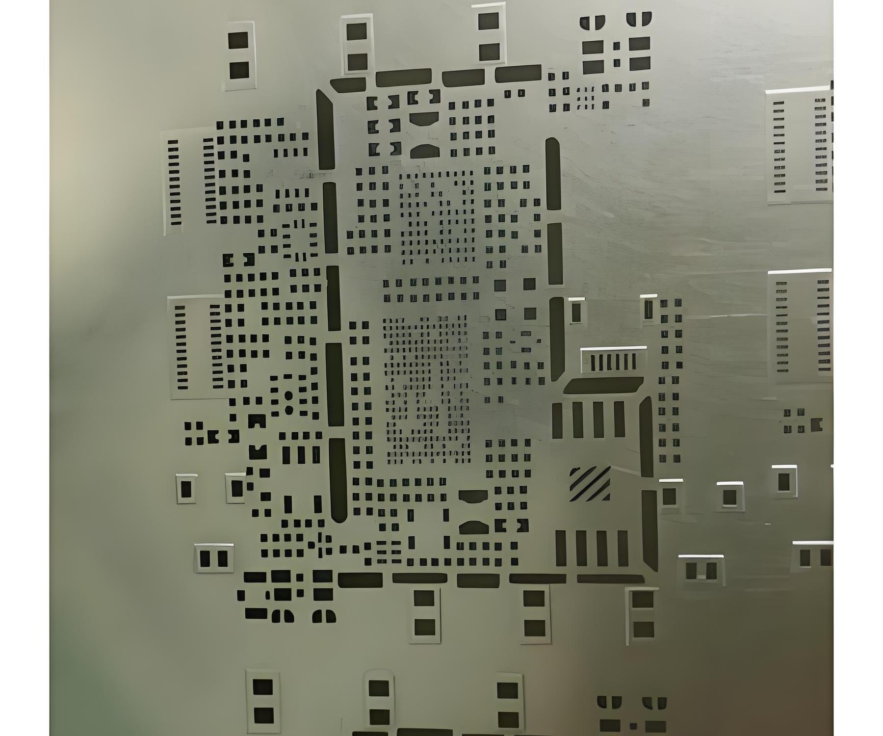
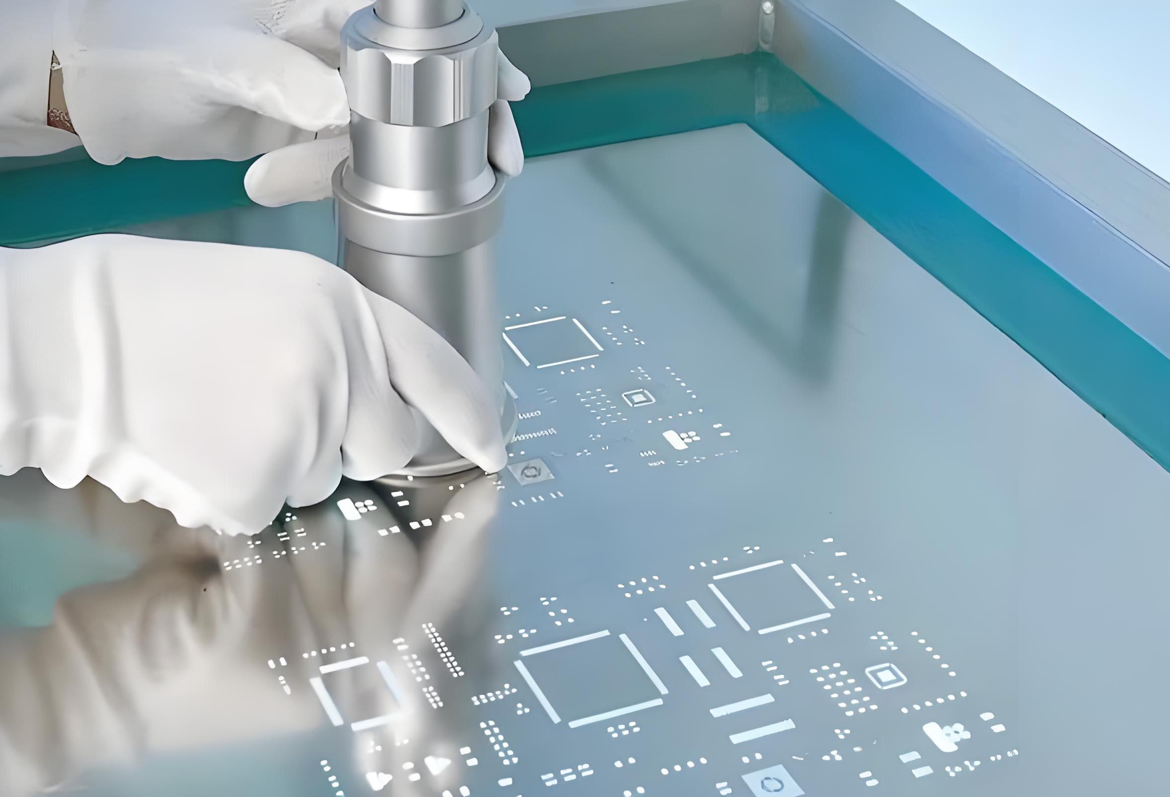
A solder paste stencil is a thin sheet used to print solder paste onto PCB pads before surface mount components are placed. It is usually made from stainless steel and has precise openings called apertures. These apertures match the solder paste layer in the PCB design files.

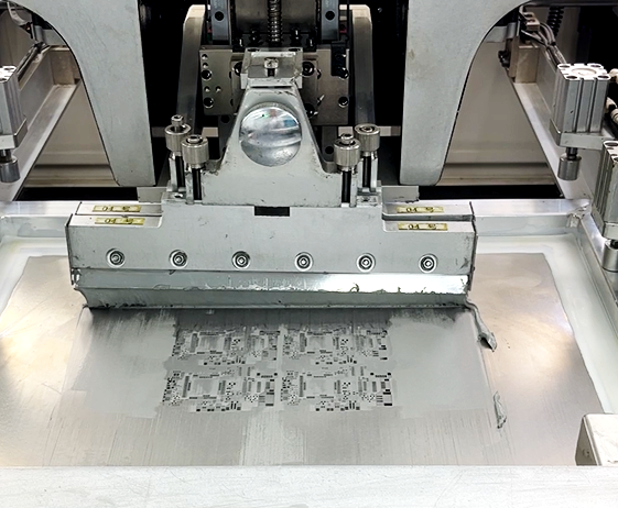
During printing, the stencil is aligned over the PCB. A squeegee pushes solder paste across the stencil surface. The paste passes through the apertures and lands on the PCB pads. After stencil separation, each pad should have a controlled solder paste deposit.

In simple terms:
A solder paste stencil controls paste volume, paste location, and printing consistency in SMT assembly.

A stencil affects:

  • Solder joint volume
  • Paste printing accuracy
  • Fine-pitch component quality
  • BGA and QFN soldering
  • LED and connector solder strength
  • SMT defect rate
  • PCBA production repeatability

For simple PCB prototypes, a standard stencil may be enough. For fine-pitch ICs, BGA packages, QFN exposed pads, 0201 components, connectors, or LED metal core PCB, stencil design needs a more detailed review.

How Does a Solder Paste Stencil Work in SMT PCB Assembly?

A solder paste stencil is used at the solder paste printing stage. This is one of the earliest and most important steps in SMT assembly. If the paste printing result is unstable, later processes such as placement, reflow, AOI, and X-ray inspection will face more risk.

A typical SMT assembly flow includes:

  • Material and PCB preparation
  • Baking when required
  • Solder paste printing
  • SPI inspection
  • Component placement
  • Reflow soldering
  • AOI inspection
  • X-ray inspection for BGA or hidden joints
  • Functional testing
  • Cleaning and final packaging

The stencil is mainly used during the solder paste printing step. However, its effect can be seen throughout the whole process.

SMT StageStencil Impact
Paste printingControls paste volume
SPIChecks paste quality
PlacementSupports stable mounting
ReflowAffects solder joints
AOIReveals visible defects
X-rayChecks hidden joints

A good stencil helps solder paste transfer cleanly from the aperture to the pad. A poor stencil may leave paste inside the opening, print too much paste, or cause offset deposits.

In production, engineers often check stencil design when defects repeat on the same pads. If the same IC pins keep bridging, or the same QFN center pad has too much solder, the stencil is usually one of the first items to review.

PCB Stencil vs Solder Paste Stencil: Are They the Same?

In most SMT projects, a PCB stencil and a solder paste stencil refer to the same tool. Both are used to print solder paste onto PCB pads.

The difference is mainly in wording.

TermMeaning
Solder paste stencilMost precise term
PCB stencilCommon buyer term
SMT stencilFactory process term
Solder stencilShorter informal term
Circuit board stencilGeneral search term

If you are ordering a stencil for assembly, “solder paste stencil” is the clearest term. It tells the supplier that the stencil is used for SMT solder paste printing, not for marking, coating, or another process.

For accurate stencil production, the supplier usually needs:

  • Gerber files
  • Paste layer
  • PCB outline
  • Fiducial marks
  • BOM
  • Pick-and-Place file
  • Assembly drawing
  • Panel drawing, if applicable

The paste layer is important, but it is not always enough. For better PCBA quality, the stencil should be checked together with component packages and assembly requirements.

What Are the Main Types of Solder Paste Stencils?

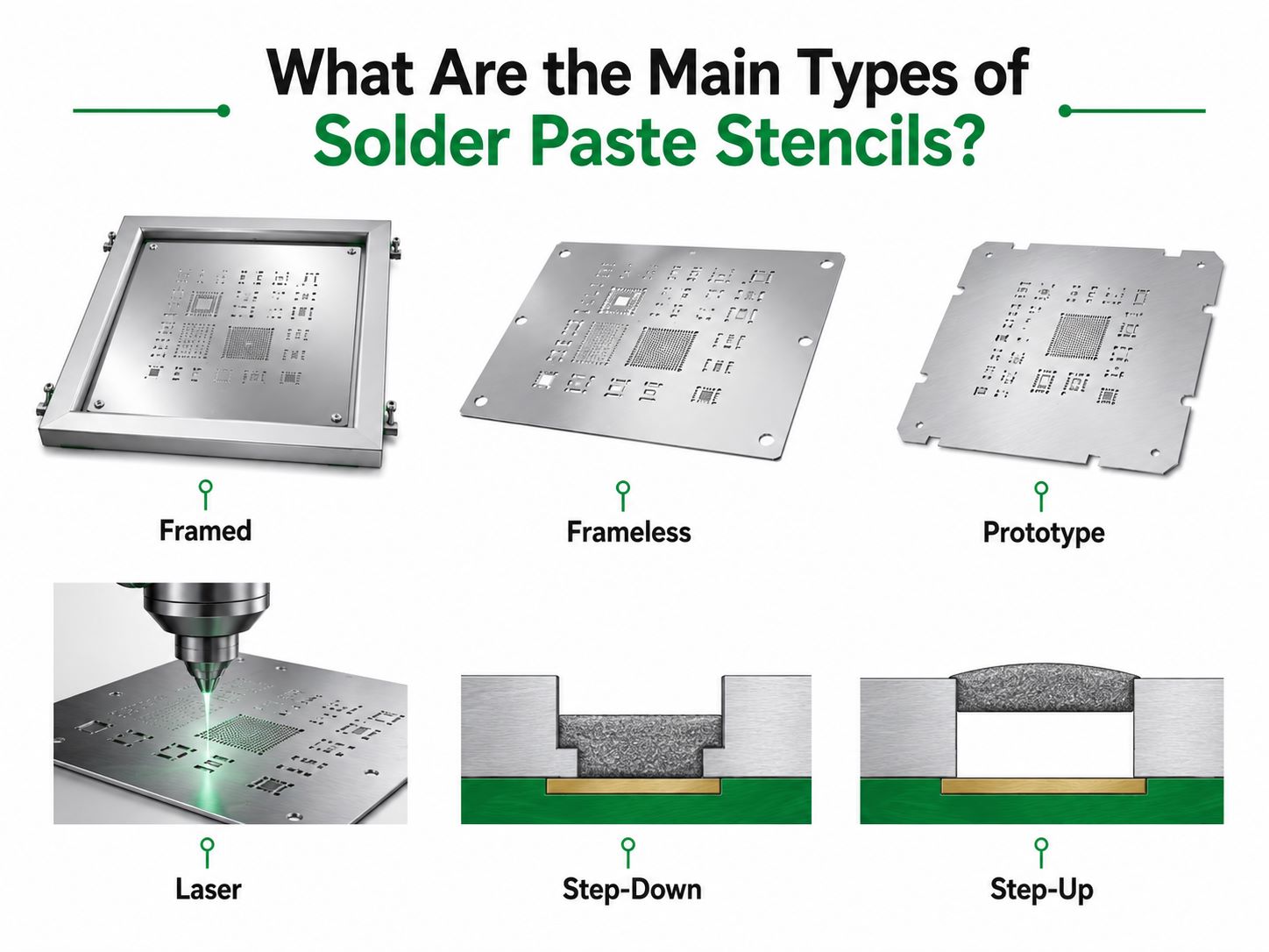
Different PCB assembly projects need different stencil types. A prototype board, a high volume PCB assembly order, and a fine-pitch BGA board may require different stencil choices.

Stencil TypeBest ForKey Value
Framed stencilMass productionStable printing
Frameless stencilLow-volume ordersFlexible use
Prototype stencilSamplesFast setup
Laser stencilFine-pitch SMTHigh accuracy
Etched stencilGeneral useCost control
Step-down stencilMixed componentsLocal paste control
Step-up stencilLarge padsExtra paste volume
BGA ball mounting stencilBGA repair or mountingBall placement
PE stencilSpecial applicationsLightweight option

Most SMT stencils today are laser cut because laser cutting offers better aperture accuracy and smoother geometry. Etched stencils are still available for some cost-sensitive or less complex applications.

For higher precision, laser cut stencils may also be electro-polished. Electro-polishing helps smooth the aperture wall and supports better solder paste release. This is especially useful for fine-pitch ICs, QFN pads, small chip components, and dense layouts.

solder paste stencil

How to Choose the Right Solder Paste Stencil Thickness?

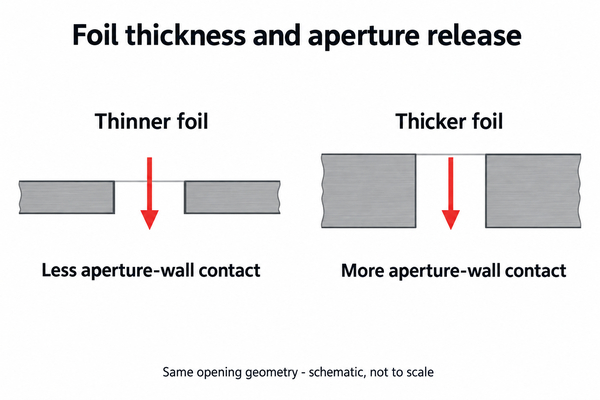
Stencil thickness controls solder paste volume. A thicker stencil prints more paste. A thinner stencil prints less paste. Choosing the right thickness is one of the most important decisions in stencil design.

Common stencil thicknesses include:

ThicknessTypical Use
0.06 mmVery fine features
0.08 mmMiniature SMT
0.10 mmFine-pitch ICs
0.12 mmStandard SMT
0.15 mmGeneral components
0.20 mmLarger pads
Up to 0.60 mmSpecial process

For most PCB assembly projects, 0.10 mm, 0.12 mm, and 0.15 mm are commonly used. The final choice depends on the smallest component, pad pitch, solder paste type, and required solder volume.

Component TypeSuggested ThicknessReason
02010.08–0.10 mmLess paste
04020.10–0.12 mmStable print
0603 / 08050.12–0.15 mmStandard volume
Fine-pitch IC0.10–0.12 mmLess bridging
QFN / DFN0.10–0.12 mmBetter control
BGA0.10–0.12 mmEven deposits
Connectors0.15 mm+More solder
LED pads0.12–0.15 mmHeat and strength
Mixed layoutStep stencilLocal control

A common problem is mixed component size. One PCB may include a fine-pitch IC and a large connector on the same side. If the whole stencil is too thick, the IC may bridge. If it is too thin, the connector may receive insufficient solder.

There are three common solutions:

  • Reduce apertures in fine-pitch areas
  • Use window-pane design on large pads
  • Use step-up or step-down stencil technology

A good stencil choice should start from the most sensitive component, then adjust aperture design for larger pads.

How Does Aperture Design Affect Solder Paste Printing?

Apertures are the openings in the stencil. They decide where solder paste goes and how much paste reaches the pad.

Stencil thickness controls paste height. Aperture design controls paste area and release behavior. Both must work together.

Important aperture design factors include:

  • Aperture size
  • Aperture shape
  • Opening ratio
  • Pad reduction
  • Corner radius
  • Aperture wall smoothness
  • Distance between apertures
  • Component package type
Aperture DesignUsed ForPurpose
1:1 openingNormal padsStandard paste
0.9:1 openingBGA areaLess excess paste
Reduced openingFine-pitch ICLess bridging
Home-plateChip partsLess solder balls
Window-paneQFN thermal padLess voiding
Rounded cornersSmall aperturesBetter release
Segmented openingLarge padsEven paste

For standard components, a 1:1 aperture may work well. For BGA areas, a 0.9:1 scale is often used to reduce excess paste and improve solder control.

For QFN or DFN exposed pads, window-pane design is usually better than one large opening. A single large aperture can print too much paste and cause the component to float during reflow. Dividing the opening into smaller windows helps control solder volume.

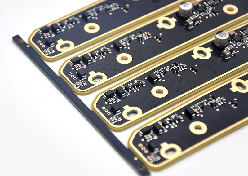
For LED metal core PCB, stencil design must also consider thermal pads, long strip board shape, and solder joint stability. Long LED strips may need special stencil support, proper panel design, and stable printing fixtures.

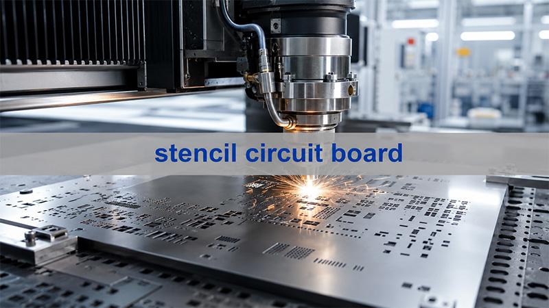
What Is a Laser Stencil?

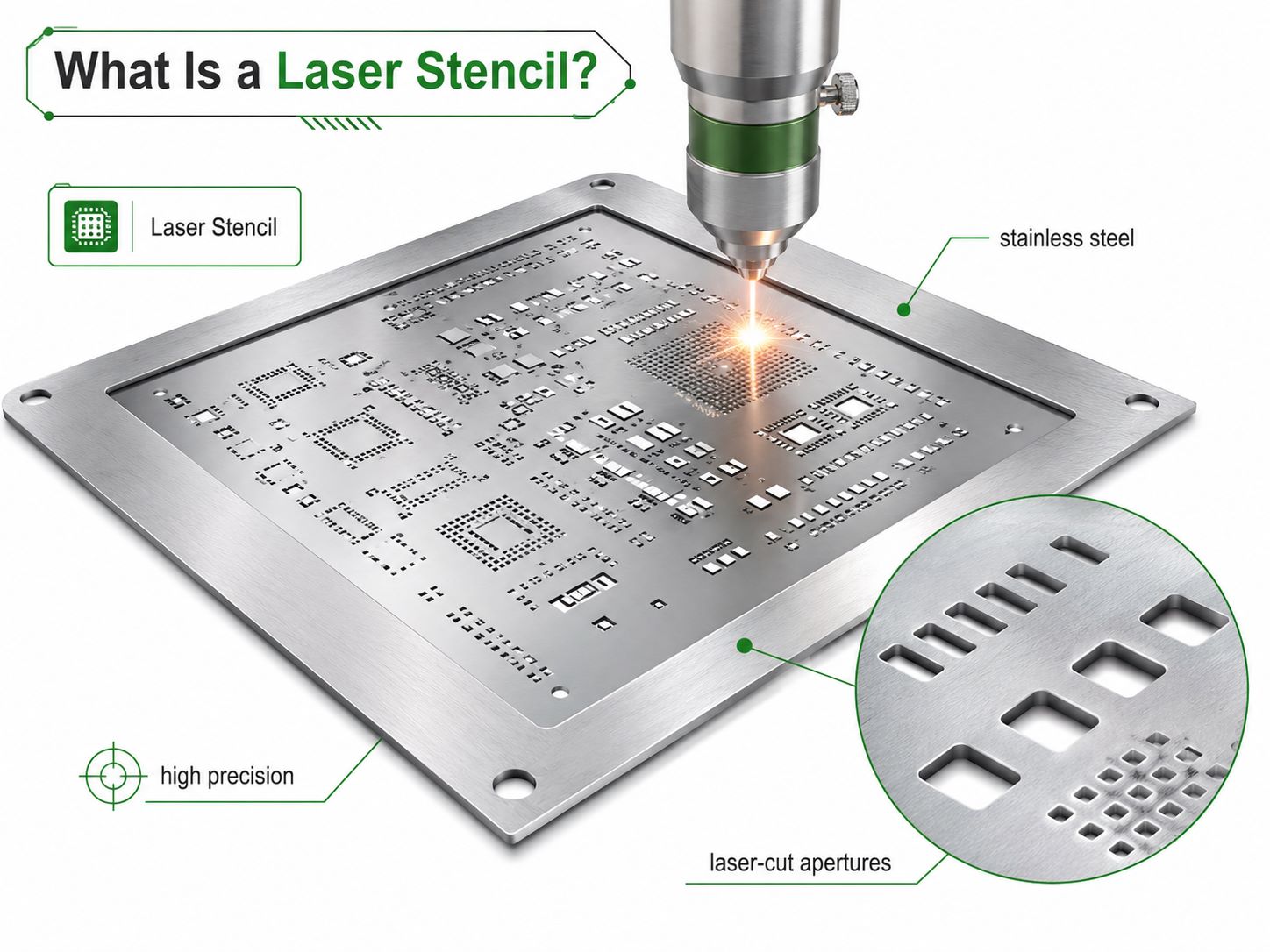
A laser stencil is a solder paste stencil made by laser cutting. The apertures are cut directly from the design data, usually from Gerber or CAD files.

Laser stencils are widely used because they offer:

  • High aperture accuracy
  • Clean opening geometry
  • Good repeatability
  • Fast production
  • Fine-pitch support
  • Compatibility with electro-polishing
  • Stable SMT printing performance

At EBest Circuit, most SMT stencils are laser cut. Etched stencils are also available when the project requirements are suitable.

Laser cut stencils are especially useful for:

  • BGA packages
  • Fine-pitch ICs
  • QFN and DFN packages
  • 0201 and 0402 components
  • High-density PCB layouts
  • Medical electronics
  • Communication modules
  • Automotive PCBA
  • Industrial control boards

For better paste release, laser cut stencils can be electro-polished. Smooth aperture walls help solder paste release more easily, reduce cleaning frequency, and improve SMT printing efficiency.

solder paste stencil

When Should You Use a Step-Down or Step-Up Stencil?

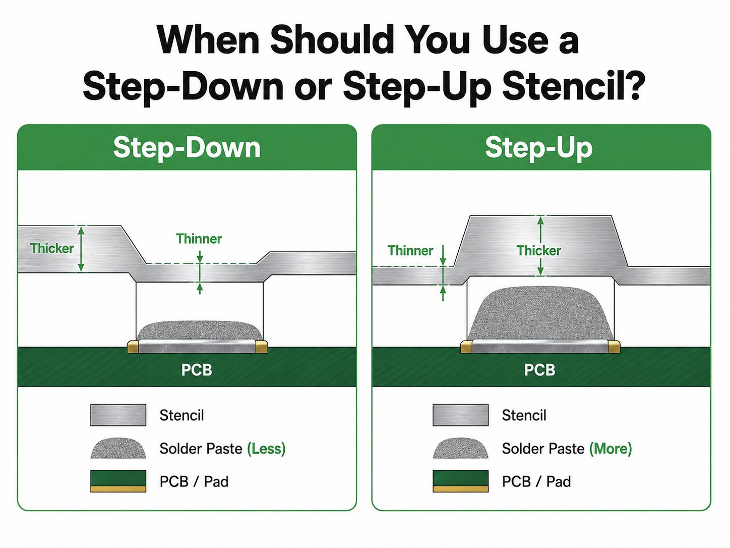
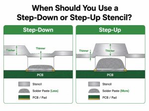
A step-down stencil has selected areas that are thinner than the main stencil. A step-up stencil has selected areas that are thicker than the main stencil.

These designs are used when different components on the same PCB need different solder paste volumes.

Stencil DesignFunctionTypical Use
Step-downLess paste locallyFine-pitch IC
Step-upMore paste locallyConnector pad
Mixed stepDifferent paste levelsComplex PCB

Use a step-down stencil when:

  • Fine-pitch ICs are bridging
  • Small components need less paste
  • QFN areas need tighter paste control
  • BGA areas require stable deposits
  • Dense layouts have limited spacing

Use a step-up stencil when:

  • Connectors need stronger joints
  • Large terminals need more solder
  • Shielding parts need higher paste volume
  • Special pads require extra solder height

Step stencil design should be reviewed carefully. The step edge should not be too close to active apertures. If the step area is too near component pads, the squeegee may not print evenly.

For many boards, aperture modification is enough. Step-up or step-down technology is more useful when aperture changes alone cannot balance solder volume.

solder paste stencil

Common Solder Paste Stencil Problems and Solutions

Many SMT defects begin at the solder paste printing stage. A good stencil can reduce these issues, but process control is also important.

DefectLikely CauseSolution
BridgingToo much pasteReduce aperture
Insufficient solderPoor releaseClean or adjust stencil
Missing pasteBlocked apertureClean stencil
Offset pasteBad alignmentCheck fiducials
TombstoningUneven pasteBalance apertures
Solder ballsExcess pasteUse better aperture
QFN floatingLarge center pasteUse window-pane
BGA openLow paste volumeCheck aperture
VoidingPoor pad designSegment aperture
Frequent cleaningRough wallsUse polishing

A stencil problem is more likely when the defect appears repeatedly in the same area. A process problem is more likely when the defect appears randomly across the board.

For example:

  • Same IC pins bridge every time: check aperture width.
  • Same QFN floats after reflow: check thermal pad opening.
  • Random missing paste: check stencil cleaning and paste condition.
  • Paste offset on many pads: check alignment and PCB support.

SPI inspection is useful here. It can check solder paste area, volume, height, thickness, short risk, and offset before components are placed. This makes stencil and printing problems easier to catch early.

How Long Can a Solder Paste Stencil Be Used?

A solder paste stencil does not last forever. In regular SMT production, its service life is usually around 50,000 prints. However, this number is not the only standard. The actual usable life depends on stencil tension, printing frequency, aperture wear, cleaning condition, storage time, and whether the stencil can still provide stable solder paste release.

In production, stencil life is usually checked by:

  • Printing count
  • Frame tension
  • Aperture wear
  • Paste release quality
  • Cleaning result
  • Storage time
  • Production history
Check ItemPractical StandardWhy It Matters
Printing countAround 50,000 printsTracks stencil usage
Stencil tensionScrap if ≤25NKeeps printing stable
Aperture wearCheck visuallyAffects paste shape
Paste releaseCheck print resultAffects solder volume
Cleaning resultNo blocked aperturesPrevents missing paste
Storage timeReview after long idle timeAvoids old tooling risk
Repeat order gapReview if no order for 3 yearsConfirms stencil reliability

For framed stencils, tension should be checked before and after use. The measurement should not be taken at only one point. It is better to check the four corners and the center area, because uneven tension can cause local solder paste printing defects.

If the stencil tension becomes weak, the printing count is over the control limit, the apertures are worn, or the stencil has been stored for too long, printing stability may decrease. For repeat PCB orders after a long gap, the old stencil should be inspected before reuse. If it no longer meets the production requirement, making a new stencil is safer than risking unstable SMT printing.

What Files Are Needed to Make a PCB Stencil?

To make a solder paste stencil, the paste layer is the key file. However, for better assembly results, the supplier should review more than one file.

FilePurpose
GerberPCB data
Paste layerAperture source
BOMPackage check
Pick-and-PlacePosition check
Assembly drawingPolarity and side
Panel drawingProduction layout
Special notesProcess needs

The required data may come from different file formats, such as Gerber, PCB, CAD, Protel, or other electrical design files.

Direct data input from customer files helps reduce manual conversion errors. It also makes stencil production faster and more accurate.

Before ordering a stencil, confirm:

  • Top side or bottom side
  • Single stencil or two stencils
  • Framed or frameless type
  • Stencil thickness
  • Fiducial marks
  • Step-up or step-down areas
  • BGA or QFN requirements
  • Long board or LED strip requirement
  • Shipping and packaging needs

For PCB assembly projects, it is better to send Gerber, BOM, and Pick-and-Place files together. This helps the engineering team check whether the stencil design matches the actual component layout.

How Does EBest Circuit Support SMT Stencil Projects?

EBest Circuit provides SMT stencil support for prototype PCB assembly, low volume PCB Assembly, and production projects. Most of our SMT stencils are laser cut. Etched stencils are also available for suitable applications.

Our stencil service covers both standard and special requirements.

CapabilitySupport
Lasercut stencilAvailable
Etched stencilOptional
Framed stencilAvailable
Frameless stencilAvailable
Stainless steel stencilStandard
PE stencilOptional
Electro-polishingAvailable
Fiducial marksCustom position
Step-up/down stencilAvailable
BGA ball mounting stencilAvailable
LED strip PCB stencilAvailable

Our stencil advantages include:

  • Fast stencil preparation after file confirmation
  • Direct use of customer design files
  • Framed and unframed stencil options
  • Stainless steel material for stable printing
  • Laser cut apertures for high accuracy
  • Electro-polished apertures for better paste release
  • Smooth opening walls to reduce cleaning frequency
  • Tapered aperture walls to support paste transfer
  • Fiducial marks based on project needs
  • Step-up and step-down options for mixed components
  • Careful packaging to protect the stencil during transport

EBest Circuit also supports PCB fabrication and SMT assembly, so stencil review can be linked with the full PCBA process. This is important because stencil quality should not be judged only by the metal sheet. It should be judged by the solder paste printing result and the final assembly quality.

For projects with BGA, QFN, fine-pitch IC, LED metal core PCB, connectors, or long strip boards, our team can review stencil thickness and aperture design before production. This helps reduce common SMT risks and improves process stability.

How to Choose a PCB Stencil Manufacturer for SMT Assembly

Choosing a PCB stencil manufacturer is not only about price. A low-cost stencil may still cause expensive rework if the aperture design, material, or thickness is not suitable.

A reliable stencil supplier should understand both stencil fabrication and SMT assembly.

Evaluation PointWhat to Check
File reviewGerber and paste layer
Thickness adviceBased on components
Aperture designFine-pitch support
Special processStep-up/down
Surface qualitySmooth release
DeliveryProduction schedule
PackagingTransport safety
Assembly feedbackSPI/AOI/X-ray link

A good supplier should be able to answer:

  • Why is this thickness selected?
  • Should the BGA aperture be reduced?
  • Does the QFN pad need window-pane design?
  • Is step-down technology necessary?
  • Is the board suitable for framed or frameless stencil?
  • Will long strip PCB need special support?
  • Can the stencil fit the SMT printer frame?

If a supplier only cuts the paste layer without checking the assembly situation, the stencil may still be usable, but it may not be optimized.

For complex PCBA projects, it is better to work with a partner who can review PCB, stencil, solder paste printing, placement, reflow, and inspection together.

Solder Paste Stencil Design Checklist

Before stencil production, use this checklist to reduce avoidable issues.

File checklist

  • Gerber files are complete
  • Paste layer is included
  • BOM is available
  • Pick-and-Place file is ready
  • Assembly drawing is clear
  • Panel drawing is confirmed

Design checklist

  • Stencil thickness is selected
  • Aperture reductions are reviewed
  • BGA areas are checked
  • QFN exposed pads are segmented
  • Fine-pitch ICs are reviewed
  • LED thermal pads are checked
  • Connector pads are reviewed

Production checklist

  • Framed or frameless type is confirmed
  • Fiducial marks are included
  • Step areas are defined
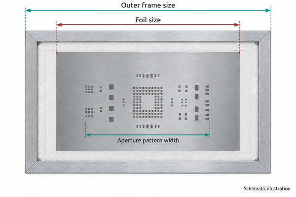
  • Printer frame size is suitable
  • PCB support method is clear
  • SPI inspection is planned
  • Packaging method is confirmed

Risk checklist

  • Mixed components on one side
  • Small 0201 or 0402 parts
  • Fine-pitch ICs
  • Large exposed pads
  • Long strip LED boards
  • Heavy connectors
  • Double-sided SMT
  • Old stencil reuse

This checklist is useful for both prototype and batch production. It helps buyers and engineers discuss stencil details before defects appear on the SMT line.

FAQs About Solder Paste Stencil

How long can a solder paste stencil be used?
A solder paste stencil can usually be used for about 50,000 prints in regular SMT production. Its actual life depends on stencil tension, print count, aperture wear, cleaning quality, and storage condition.

When should an SMT stencil be scrapped?
An SMT stencil should be scrapped if the measured tension is ≤25N, if the print count exceeds 50,000 cycles, or if it has not been used for a customer order for around 3 years. In these cases, the stencil may no longer provide stable solder paste printing.

How should stencil tension be checked?
Stencil tension should be checked before and after use. The measurement should cover the four corners and the center area, not just one point, because uneven tension can cause local printing defects.

What solder paste printing problems can SPI detect?
SPI can detect solder paste volume, area, thickness, height, depth, offset, and short-circuit risk. It helps catch printing issues such as missing paste, offset paste, solder bridging, insufficient solder, and paste peaks before component placement.

What are common solder paste stencil thicknesses?
Common stencil thicknesses include 0.06mm, 0.08mm, 0.10mm, 0.12mm, 0.15mm, and 0.20mm. For many SMT PCB assembly projects, 0.10mm, 0.12mm, and 0.15mm are frequently used, while special designs may require thinner, thicker, or step-up/down stencils.

On the whole, a solder paste stencil is a key process tool in SMT PCB assembly. It controls solder paste volume, printing accuracy, aperture release, and the first condition for good solder joints.

A suitable stencil should match the PCB design, component package, paste type, production volume, and inspection requirements. For simple boards, a standard laser stencil may be enough. For fine-pitch ICs, BGAs, QFNs, connectors, LED metal core PCB, or mixed component layouts, stencil thickness and aperture design should be reviewed carefully.

EBest Circuit provides solder paste stencil support together with PCB fabrication and PCB assembly services. We support laser cut stencils, etched stencils, framed and frameless stencils, electro-polished apertures, fiducial marks, step-up/down technology, BGA ball mounting stencils, and stencil solutions for long strip LED metal core PCB.

If your project requires a solder paste stencil or complete SMT PCB assembly, you can send your Gerber files, BOM, Pick-and-Place file, and assembly requirements to sales@bestpcbs.com. Our engineering team can help review the stencil design before production and support your project from prototype to batch assembly.

You may also like

Stencil Circuit Board: How to Choose the Right PCB Stencil for Reliable SMT Assembly
Wednesday, May 6th, 2026

A stencil circuit board usually refers to a PCB solder paste stencil used to print solder paste onto a circuit board before SMT assembly. In this process, a thin stainless steel stencil is aligned over the PCB, and solder paste is pushed through small laser-cut openings onto the surface-mount pads. This step matters because solder paste volume and position directly affect solder joint quality, fine-pitch component reliability, and overall PCBA yield.

This guide covers PCB stencil basics, solder paste printing, stencil types, thickness selection, laser stencil benefits, common SMT defects, and practical design rules for better assembly quality.

At EBest Circuit, we treat stencil design as part of the complete SMT PCBA process, not as a separate accessory. Our team reviews Gerber files, BOM data, component packages, PCB surface finish, and assembly requirements to help customers reduce solder defects and improve production consistency from prototype to batch assembly. For stencil-related PCB assembly support, you can send your files or questions to sales@bestpcbs.comfor a practical engineering review.

Stencil Circuit Board

What Is a Stencil Circuit Board and How Is It Used in SMT Assembly?

A stencil circuit board usually refers to the solder paste printing process used before SMT assembly. In professional PCB manufacturing, the stencil is not the circuit board itself. It is a precision tool placed over the PCB to print solder paste onto the surface-mount pads.

In the PCB industry, this tool may also be called a PCB stencil, solder stencil, solder paste stencil, circuit board stencil, or printed circuit board stencil. These terms usually describe the same item when people are talking about SMT assembly.

The stencil has small laser-cut openings called apertures. These apertures match the SMT pads on the printed circuit board. During printing, solder paste is pushed across the stencil with a squeegee. The paste passes through the apertures and forms controlled deposits on the PCB pads. After that, SMT components are placed onto the paste and soldered during the reflow process.

This step may look simple, but it directly affects solder joint quality. A good PCB stencil controls where the paste goes, how much paste is deposited, and how consistent the paste volume remains across the board. If the stencil design or printing process is not well controlled, defects such as solder bridging, insufficient solder, tombstoning, solder balls, open joints, or unstable fine-pitch assembly may appear.

A well-designed solder paste stencil helps improve:

  • Solder paste position accuracy
  • Solder paste volume consistency
  • Fine-pitch component assembly
  • Reflow solder joint reliability
  • First-pass yield
  • SMT production repeatability
  • Rework reduction

For prototype boards, engineers may use a frameless solder stencil and apply paste manually. For medium and high-volume production, a framed laser stencil and a printed circuit board stencil printer are more suitable because they provide better tension, alignment, and repeatability.

In commercial PCB assembly, the stencil should be reviewed together with the PCB layout, BOM, component package types, board finish, and assembly process. A PCB stencil is not only a paste application tool. It is part of the SMT process control system. A well-designed stencil gives the assembly line a cleaner starting point and helps the whole production flow run more smoothly.

What Are the Main Types of PCB Stencils?

Different PCB projects need different stencil types. The right choice depends on production volume, component density, pad geometry, board size, and printing method.

PCB Stencil TypeBest ForMain AdvantageTypical Application
Framed PCB stencilMedium to high-volume productionStable tension and repeatable printingAutomatic SMT stencil printer
Frameless PCB stencilPrototype and small batch assemblyLower cost and easy storageManual printing or reusable frame
Laser stencilMost professional SMT projectsAccurate apertures and clean paste releaseFine-pitch SMT assembly
Step stencilMixed component paste volume needsDifferent thickness in selected areasBoards with small ICs and large connectors
Nano-coated stencilDense or high-reliability boardsBetter paste release and easier cleaning0201, QFN, BGA, fine-pitch ICs
Rework stencilLocal component repairApplies paste to one selected areaBGA, QFN, connector repair

For most modern SMT projects, a stainless steel laser stencil is the preferred option. It offers better aperture accuracy than low-cost plastic or manually cut stencils. This matters when the board includes fine-pitch ICs, small passives, QFNs, BGAs, or compact modules.

For early prototypes, a simple solder stencil may be enough. For repeat production, a more controlled stencil design is usually worth the investment.

Framed vs. Frameless PCB Stencil: Which One Should You Choose?

One of the most common decisions is whether to choose a framed or frameless PCB stencil.

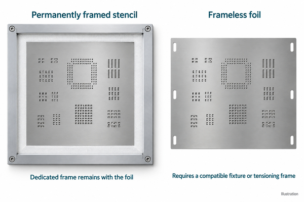
A framed PCB stencil is mounted permanently inside an aluminum frame. The frame keeps the stencil under tension, which helps maintain flatness during printing. This type is widely used with automatic or semi-automatic stencil printers.

A frameless PCB stencil is a stainless steel sheet without a permanent frame. It is lighter, easier to ship, and usually more affordable. It can be used manually or placed into a reusable tensioning frame.

ItemFramed PCB StencilFrameless PCB Stencil
CostHigherLower
Printing stabilityExcellentGood with proper fixture
Storage spaceLargerCompact
Best volumeMedium to high volumePrototype to small batch
Typical methodAutomatic stencil printerManual or semi-automatic printing
RepeatabilityStrongDepends on fixture and operator
ShippingHeavierEasier and cheaper

Choose a framed stencil if your project needs repeat production, stable paste printing, and automated SMT assembly.

Choose a frameless stencil if your project is still in prototype validation, small batch testing, or engineering verification.

For companies moving from prototype to volume production, it is common to start with a frameless stencil and later switch to a framed laser stencil once the PCB design is stable.

Why Are Laser-Cut Stencils Preferred for Fine-Pitch SMT Components?

A laser-cut stencil is made by cutting apertures into stainless steel according to the PCB paste layer. Compared with simple plastic stencils or low-precision cutting methods, laser cutting provides much cleaner aperture geometry.

Fine-pitch SMT components need very controlled solder paste deposits. If the aperture is rough, too large, or poorly shaped, paste release becomes unstable. This can affect IC pins, small passive components, QFN pads, BGA pads, and high-density layouts.

Laser-cut PCB stencils are preferred because they offer:

  • More accurate aperture size
  • Cleaner aperture walls
  • Better solder paste release
  • Improved fine-pitch printing
  • Stronger repeatability
  • Better support for small SMT packages
  • Less risk of paste smearing

For 0201 components, 01005 components, QFNs, BGAs, and fine-pitch connectors, aperture wall quality matters. Smooth aperture walls help solder paste release cleanly from the stencil instead of sticking inside the openings.

For advanced assemblies, nano-coating can also be added to the stencil surface. This improves paste release and reduces cleaning frequency, especially when the stencil has many small apertures.

What Stencil Thickness Should You Use for a Circuit Board?

Stencil thickness controls solder paste volume. A thicker stencil deposits more paste. A thinner stencil deposits less paste and is often better for fine-pitch components.

There is no single stencil thickness that fits every PCB. The right thickness depends on component package types, pad size, board design, and assembly requirements.

Stencil ThicknessCommon Use
0.08 mm / 3 milUltra-fine pitch, 01005, very small pads
0.10 mm / 4 milFine-pitch ICs, 0201 components
0.12 mm / 5 milGeneral SMT assembly with moderate density
0.15 mm / 6 milStandard SMT boards with larger components
0.18 mm / 7 mil or aboveHigh paste volume pads, larger terminals, special applications

For many standard SMT boards, 0.12 mm or 0.15 mm is common. However, boards with very small components may need thinner stencils to avoid excess paste. Boards with large connectors, power components, or shield pads may need more paste.

This creates a challenge when one PCB has both tiny fine-pitch components and large pads. In that case, a step stencil may be a better choice. A step stencil allows selected areas to be thinner or thicker, so each component receives the right paste volume.

Stencil thickness should not be selected only by habit. It should be reviewed according to the actual PCB design.

What Are Common SMT Printing Defects and How Can a Quality Stencil Fix Them?

Many SMT defects begin during solder paste printing. A quality stencil cannot replace good process control, but it gives the assembly process a much better starting point.

SMT Printing DefectCommon CauseHow a Better Stencil Helps
Solder bridgingToo much paste or poor aperture designReduces excess paste and improves aperture control
Insufficient solderSmall aperture, poor paste transfer, clogged openingsImproves paste release and deposit consistency
TombstoningUneven paste volume or thermal imbalanceSupports balanced paste deposits on both pads
Solder ballsExcess paste, smearing, poor cleaningImproves edge definition and print cleanliness
Open jointsLow paste volume or poor contactHelps maintain proper paste height
QFN voidingPoor thermal pad paste designUses windowpane aperture design for better outgassing
Paste misalignmentPoor stencil positioning or unstable fixtureFramed stencil and printer alignment improve repeatability

For example, QFN thermal pads should not always be printed as one large solder paste block. A segmented windowpane pattern can improve paste control and reduce voiding. Fine-pitch IC pads may need aperture reduction to prevent bridging. Large pads may need modified openings to avoid floating or excessive solder.

Good stencil design is practical engineering work. It is not only file processing.

Manual vs. Automatic PCB Stencil Printing: Which Method Fits Your Project?

PCB stencil printing can be done manually, semi-automatically, or with an automatic printed circuit board stencil printer. The best method depends on your project stage and production volume.

Manual printing is common for prototypes. The operator aligns the stencil with the PCB, applies solder paste, and uses a squeegee to spread the paste across the stencil. This method is flexible and affordable, but it depends heavily on operator skill.

Automatic stencil printing is used in professional SMT production. A printed circuit board stencil printer controls alignment, squeegee pressure, print speed, stencil separation, and cleaning cycles. For dense boards or repeated production, this method gives much better consistency.

Printing MethodBest ForAdvantageLimitation
Manual stencil printingPrototypes and simple boardsLow cost and quick setupOperator-dependent
Semi-automatic printingSmall to medium batchesBetter control than manual printingStill needs setup skill
Automatic stencil printingVolume SMT productionHigh repeatability and throughputHigher equipment cost

Some search terms describe this equipment as an SMT PCB solder paste stencil printing circuit board printing machine. In production language, it is usually called an SMT stencil printer or solder paste printer.

For commercial PCB assembly, automatic stencil printing is usually preferred because it reduces variation between boards. This is especially important for medical electronics, industrial control boards, communication modules, automotive electronics, and other reliability-focused applications.

How Should You Use a Solder Stencil Squeegee Correctly?

The solder stencil squeegee has a direct effect on paste filling and print quality. Even with a good stencil, poor squeegee technique can cause incomplete deposits, smearing, or inconsistent paste height.

Several factors should be controlled during the solder stencil squeegee circuit board process.

Squeegee angle
A typical angle is around 45° to 60°. This helps the solder paste roll smoothly across the stencil and fill the apertures properly.

Printing pressure
Pressure should be enough to wipe the stencil surface clean and fill the apertures. Too much pressure may scoop paste out of openings or damage the stencil over time.

Printing speed
A stable speed helps maintain a smooth paste roll. Very fast printing may leave incomplete deposits, while very slow printing may affect paste behavior.

Paste condition
Solder paste should be stored, warmed, and mixed according to supplier recommendations. Paste that is too dry or poorly handled can affect release quality.

PCB support
The board should be fully supported under the stencil. If the PCB flexes during printing, solder paste thickness may become uneven.

Stencil separation
After printing, the stencil should lift away cleanly. Good separation helps keep the paste deposit shape intact.

For manual prototype printing, it is helpful to use a flat fixture, proper board stops, and steady squeegee movement. For production, the printer should control pressure, speed, alignment, and cleaning cycle.

What PCB Stencil Design Rules Should Engineers Check Before Ordering?

Before ordering a circuit board stencil, engineers should review more than the paste layer. The stencil must match the actual assembly process.

Important checks include:

  • Correct Gerber paste layer
  • Accurate PCB outline
  • Proper fiducials for alignment
  • Suitable stencil thickness
  • Aperture reduction for fine-pitch ICs
  • Rounded aperture corners for better paste release
  • Windowpane design for QFN thermal pads
  • Paste opening adjustment for large pads
  • Step stencil requirement for mixed components
  • Panelized PCB compatibility
  • Tooling holes and rail clearance
  • Nano-coating requirement for dense apertures
  • Component package review
  • Special notes for selective assembly

A PCB stencil should not always copy the CAD paste layer exactly. Some apertures need adjustment to improve manufacturability. For example, large exposed pads may need segmented openings, while fine-pitch pads may need reduced aperture width.

Engineers should also check the aperture area ratio. If the aperture is too small relative to stencil thickness, solder paste may not release well. This is one reason thin stencils are often used for small components.

For complex PCB assemblies, stencil review should be included in DFM before production begins.

How Should PCB Stencils Be Cleaned and Maintained?

Stencil cleaning and storage affect long-term printing quality. Even a well-made stencil can create defects if solder paste dries inside the apertures or residue remains on the surface.

Good stencil maintenance includes:

  • Clean the stencil after use
  • Use compatible cleaning solvents
  • Remove paste from aperture walls
  • Avoid scratching the stencil surface
  • Store the stencil flat or in a protected rack
  • Keep framed stencils away from impact
  • Inspect for damaged apertures
  • Follow printer cleaning intervals
  • Control paste drying during long print runs

Fine-pitch stencils need closer cleaning control because small apertures clog more easily. If paste does not release fully, the printed pads may receive less solder than expected.

For production lines, under-stencil cleaning is often scheduled after a certain number of prints. The interval depends on solder paste type, stencil design, aperture density, and process requirements.

A clean stencil supports more stable solder paste deposits and better SMT yield.

Why Choose EBest Circuit for PCB Stencil and SMT Assembly Support?

Choosing the right PCB stencil is important, but stencil quality works best when it is connected with the full SMT assembly process. The stencil, solder paste, PCB finish, component package, printer setup, placement accuracy, reflow profile, and inspection plan all need to work together.

EBest Circuit, also known as Best Technology, supports PCB fabrication, PCB assembly, component sourcing, DFM review, SMT assembly, testing, and box-build services. For stencil-related projects, the engineering team can review Gerber files, BOM, pick-and-place files, and assembly drawings before production.

EBest Circuit can support:

  • Custom PCB fabrication
  • Solder paste stencil preparation
  • Laser stencil support
  • SMT assembly
  • Component sourcing
  • BOM optimization
  • DFM review
  • AOI inspection
  • X-ray inspection
  • Functional testing
  • Prototype and batch production
  • Engineering support for fine-pitch assembly

For customers working on medical electronics, industrial control, communication devices, automotive electronics, battery charger PCBs, IoT products, and power electronics, stencil design is part of the broader manufacturing quality plan. If your PCB has fine-pitch components, QFNs, BGAs, 0201 parts, dense routing, or strict reliability requirements, it is better to review stencil requirements before production starts. For custom PCB stencil or SMT assembly support, please feel free to send your Gerber files, BOM, and assembly requirements to sales@bestpcbs.com. The EBest Circuit team will be glad to review your project and provide a practical quotation.

FAQs About Stencil Circuit Board

1. What is a stencil circuit board?

A stencil circuit board usually refers to the solder paste printing process used for SMT assembly. A PCB stencil is placed over the board, and solder paste is printed through the stencil openings onto the SMT pads.

2. Is a PCB stencil necessary for SMT assembly?

Yes, a PCB stencil is strongly recommended for SMT assembly. It helps apply solder paste accurately and consistently, especially when the board has fine-pitch ICs, small passive components, QFNs, or BGAs.

3. What is the difference between a solder stencil and a PCB stencil?

In most SMT assembly discussions, solder stencil and PCB stencil mean the same thing. Both refer to the stencil used to apply solder paste onto printed circuit board pads.

4. What is a laser stencil?

A laser stencil is a stainless steel PCB stencil with apertures cut by laser. It provides accurate openings, smooth aperture walls, and reliable solder paste release for SMT assembly.

5. What stencil thickness should I choose?

Common PCB stencil thickness ranges from 0.08 mm to 0.18 mm. Standard SMT boards often use 0.12 mm or 0.15 mm, while fine-pitch boards may need thinner stencils.

6. What is a framed PCB stencil?

A framed PCB stencil is mounted inside an aluminum frame. It provides stable tension and is commonly used with automatic stencil printers for repeat production.

7. What is a frameless PCB stencil?

A frameless PCB stencil is a stainless steel stencil sheet without a permanent frame. It is often used for prototypes, small batches, or reusable frame systems.

8. Can I use a DIY solder paste stencil?

A DIY stencil may work for simple hobby boards with large components. For professional PCB assembly, a stainless steel laser-cut stencil is usually better because it provides stronger accuracy and repeatability.

9. How do you cover unused openings in a PCB stencil?

Unused stencil openings can be temporarily covered with Kapton tape. For repeat production, it is better to revise the paste layer and make a corrected stencil.

10. What causes solder bridging during stencil printing?

Solder bridging may happen when too much paste is printed, stencil thickness is unsuitable, aperture design is not optimized, or the stencil is misaligned.

11. What files are needed to order a PCB stencil?

Most suppliers need the Gerber paste layer, PCB outline, fiducial information, and panel data. For full SMT assembly review, BOM and pick-and-place files are also useful.

12. Are circuit board paint stencils the same as PCB solder stencils?

No. A circuit board paint stencil or circuit board airbrush stencil is usually used for decoration or artwork. A PCB solder stencil is a manufacturing tool used to apply solder paste during SMT assembly.

You may also like

Your Trusted SMT Stencil Manufacturer – Precision & Reliability
Tuesday, January 27th, 2026

When searching for a professional SMT stencil manufacturer, BestPCBS stands out as the top choice for electronic manufacturers worldwide. Our decades of expertise in producing high-precision stencils make us the most reliable SMT stencil manufacturer for all your surface mount technology needs, from prototyping to mass production.

Why BestPCBS Is Your Top Choice for an SMT Stencil Manufacturer?

At BestPCBS, we combine advanced manufacturing technology with strict quality control to deliver SMT stencils that meet the highest industry standards. We offer 24/7 customer support, customizable solutions, and competitive pricing—factors that make us the preferred SMT stencil manufacturer for SMEs and large enterprises alike. Our on-time delivery rate exceeds 98%, ensuring your production lines never face delays.

Our Core Advantages

  • Precision: ±5μm aperture tolerance for fine-pitch components (01005, BGA, QFP)
  • Speed: 24-hour expedited service for urgent SMT stencil orders
  • Cost: 15% lower production costs compared to industry averages
  • Support: Dedicated engineering team for DFM reviews and technical guidance
SMT Stencil Manufacturer

What Defines a High-Quality SMT Stencil Manufacturer?

A high-quality SMT stencil manufacturer must master both technical precision and customer-centric service. At BestPCBS, we adhere to ISO 9001:2015 quality management standards, conducting 3 rounds of inspection before shipping any stencil. This commitment to quality ensures our stencils reduce solder defects by up to 70% for our clients.

4 Core Processes We Use for Custom SMT Stencil Manufacturing

Our custom SMT stencil manufacturing process is tailored to your specific PCB design requirements. We use four proven processes to cover all application scenarios, ensuring optimal solder paste transfer and long stencil lifespan:

ProcessPrecisionIdeal For
Laser Cutting≤5μmHigh-volume production
Electroforming≤3μmUltra-fine pitch components
Chemical Etching≤10μmLow-cost prototypes
Hybrid Process≤4μmMixed-technology PCBs

How We Ensure High-Precision SMT Stencil Production at BestPCBS

High-precision SMT stencil production starts with advanced equipment and skilled engineers. We use CNC laser cutters and 3D measuring systems to verify every aperture, ensuring positional accuracy within ±2μm. This level of precision directly improves PCB assembly yield by 10-15% for our customers.

Industrial-Grade Materials for Durable SMT Stencils

We only use industrial-grade SUS301 and SUS304 stainless steel for our SMT stencils, providing 400,000+ printing cycles per stencil—20% more than standard materials. For flexible PCB applications, we offer Kapton stencils with reinforced edges for added durability.

SMT Stencil Quality Inspection Standards at BestPCBS

Our SMT stencil quality inspection process includes three critical steps: dimensional verification, tension testing (35-50N/cm²), and surface finish inspection. Every stencil is tested on a dummy PCB to confirm solder paste transfer efficiency before delivery, eliminating post-shipping issues.

How to Reduce SMT Stencil Costs Without Compromising Quality

SMT stencil cost optimization is a key focus at BestPCBS. We offer bulk pricing discounts, design optimization suggestions to reduce material waste, and reusable stencil frames to lower long-term costs. Our engineering team reviews your PCB design for free to identify cost-saving opportunities without sacrificing performance.

Short Lead Time for SMT Stencils: Our Expedited Service

We understand the urgency of production deadlines, which is why our SMT stencil lead time starts at 24 hours for expedited orders and 3-5 business days for standard orders. We offer free express shipping on all expedited orders, ensuring your stencils arrive on time, every time.

FAQ: Common SMT Stencil Issues & BestPCBS’s Solutions

Q1: Why is my SMT stencil causing solder bridges?

A: Solder bridges are often caused by oversized apertures or poor surface finish. We calibrate aperture sizes based on your solder paste type and offer electro-polished stencils to reduce solder adhesion, eliminating bridge defects.

Q2: How can I extend the life of my SMT stencil?

A: Regular cleaning with ultrasonic cleaners and proper storage (23±3°C, 40-60% humidity) extends stencil life. We provide a free maintenance guide with every order to help you maximize stencil usage.

Q3: Can you modify an existing SMT stencil?

A: Yes, our engineering team can modify apertures or repair minor damage to existing stencils, saving you the cost of a full replacement. Modifications are completed within 12 hours for urgent requests.

Q4: Do you offer DFM reviews for SMT stencil designs?

A: Yes, we provide free SMT stencil design for manufacturability reviews to identify potential printing issues before production, reducing rework and delays.

Q5: What after-sales support do you provide?

A: We offer a 30-day warranty on all stencils and 24/7 technical support. Our team can assist with stencil installation, cleaning, and troubleshooting via video call or email.

SMT Stencil Design for Manufacturability (DFM) Guidelines

Our SMT stencil design for manufacturability guidelines help optimize your PCB design for efficient stencil production. We recommend aperture sizes 1.5x the stencil thickness, rounded aperture corners to reduce stress, and spacing guidelines for fine-pitch components to avoid printing defects.

After-Sales Support for Our SMT Stencil Customers

Our SMT stencil after-sales support doesn’t end with delivery. We offer free technical training for your production team, stencil repair services, and replacement parts for frames and gaskets. Our customer support team responds to all inquiries within 1 business hour.

Case Studies: Successful SMT Stencil Projects by BestPCBS

We’ve supplied SMT stencils to leading electronics manufacturers in automotive, medical, and consumer electronics industries. One medical device client saw a 25% reduction in solder defects after switching to our high-precision stencils, while an automotive client reduced production downtime by 30% with our short lead time service.

SMT stencil manufacturer

sales@bestpcbs.com

If you’re currently using an SMT stencil manufacturer that doesn’t meet your quality, speed, or cost requirements, it’s time to switch to BestPCBS. We offer a free sample stencil (up to 100x100mm) for new customers to test our quality firsthand. Contact us at sales@bestpcbs.com to place your order or request a quote—our team is ready to help you optimize your SMT stencil supply chain today.

You may also like

PCB Stencil: What is Stencil in PCB & How to Use PCB Stencil
Tuesday, February 18th, 2025

What is a Stencil in PCB?

A PCB stencil is a precision tool used in the process of assembling printed circuit boards. Its main function is to apply solder paste to the board in a controlled manner, ensuring the paste only reaches the pads where components will be mounted. By creating uniform paste deposits, the stencil facilitates the correct soldering of components during the assembly process, contributing significantly to the quality and reliability of the final product.

PCB Stencil: What is Stencil in PCB & How to Use PCB Stencil

What Does a Stencil Do?

A PCB stencil plays several crucial roles in the PCB assembly process, including:

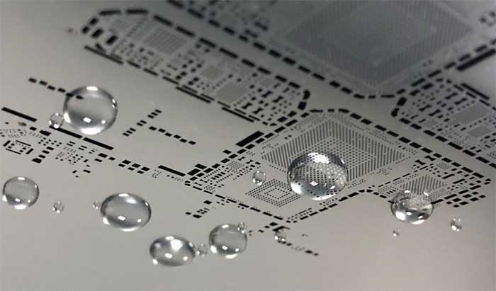
1. Applies Solder Paste: The primary function of a stencil is to accurately apply solder paste to the PCB. The paste is deposited onto the pads of the PCB through the openings in the stencil, ensuring the right amount of paste is used for each component.

2. Improve Precision: By using a stencil, manufacturers can achieve highly precise solder paste placement. This is especially important for fine-pitch components, where precision is key to avoiding defects like bridging or insufficient solder.

3. High Efficiency: Stencils speed up the solder paste application process, making it more efficient than manual paste application. This is particularly beneficial in high-volume manufacturing, where consistency and speed are vital.

4. Reduces Human Error: Using a stencil minimizes the chances of human error in solder paste application. This leads to more consistent and reliable results, reducing the likelihood of defects in the final product.
5. Facilitates High-Volume Production: Stencils are essential for mass production, allowing manufacturers to quickly and efficiently apply paste across multiple PCBs with high consistency.

6. Improves Reflow Soldering: With the right amount of solder paste applied, the stencil helps ensure that the reflow soldering process is carried out effectively, leading to strong and durable solder joints.

What is a PCB Stencil Consist of?

A PCB stencil consists of several crucial components that work together to ensure precise solder paste application. These elements include:
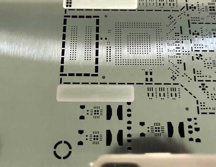
1. Frame

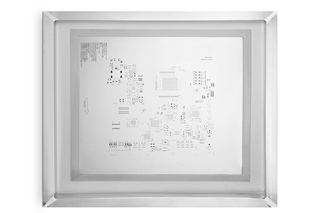
The frame is essential for holding the stencil in place during the application process. It is categorized into movable frames and fixed frames. The movable frame attaches the steel plate directly to the frame, allowing the template to be reused. On the other hand, the fixed frame uses adhesive to attach the wire mesh to the formwork. For optimal performance, a strong frame with uniform steel tension—typically between 35 and 48 N/cm²—is preferred. The normal fixed frame tension is between 35 N to 42 N, ensuring stability and accuracy.

2. Sheet Plates

High-quality stainless steel plates such as 301/304 stainless steel are commonly used because they offer excellent mechanical properties, significantly increasing the service life of the stencil. Other materials such as copper plates, nickel alloy, and polyester may also be used, depending on the specific application requirements.

3. Mesh

The mesh is used to fix the steel plates and formwork in place. There are two main types of mesh: stainless steel mesh and polymer polyester mesh. Stainless steel mesh is typically around 100 mesh and ensures stable tension, but it can deform and lose tension over time. Polyester mesh, on the other hand, is made from an organic fabric that doesn’t easily deform and has a longer service life, making it a more durable option for long-term use.

4. Adhesive (Glue)

The glue used in PCB stencils serves as the binding material that attaches the trellis frame to the steel sheet. It is an essential part of maintaining the integrity and stability of the stencil. The adhesive used needs to provide strong adhesion and be able to withstand heavy cleaning with various plate cleaners without losing its effectiveness.

Together, these components—frame, sheet, mesh, and glue—combine to form a PCB stencil that ensures accurate, consistent, and efficient solder paste application during the PCB assembly process.

What Are the Different Types of Stencils?

There are various types of PCB stencils, each designed for specific applications and production requirements:

  • Laser-Cut Stencils: These are the most accurate and commonly used type. Laser cutting provides high precision, making these stencils perfect for fine-pitch components or designs with intricate details.
  • Etched Stencils: Etching is an older method but still used for simpler projects. Though less precise than laser-cut stencils, etched stencils are still valuable for projects where absolute precision is not as critical.
  • 3D Printed Stencils: 3D printing technology has opened up a new avenue for creating PCB stencils. This method is ideal for low-volume or prototype PCB assembly, offering flexibility and faster turnaround times for custom designs.
  • DIY Stencils: For hobbyists or small-scale production, DIY methods using materials like adhesive-backed foil or plastic sheets can be used to create simple stencils. These are cost-effective but come with trade-offs in precision and durability.
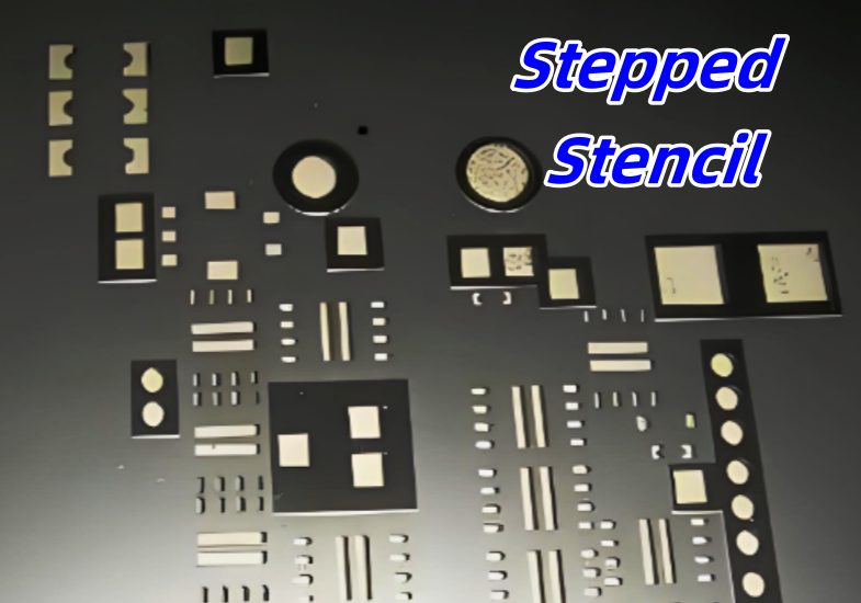
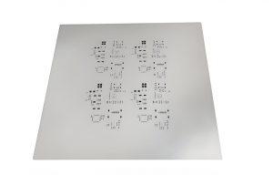
  • Stepped Stencil: A stepped stencil features varying thicknesses across different areas of the stencil. These thickness changes, or “steps,” allow the stencil to deposit different amounts of solder paste for different components on the same PCB. Stepped stencils are particularly useful when there is a mix of fine-pitch components and larger, more spaced-out components on the same board. Below is a typical photo of stepped stencil.
PCB Stencil: What is Stencil in PCB & How to Use PCB Stencil

PCB Stencil HS Code

The HS code for PCB stencils is 7314490000.

This code is specifically used for steel product, which includes PCB stencils used in the manufacturing process. It’s important to use the correct HS code for shipping and customs purposes to ensure smooth international transactions.

Warm Notice:

It’s always advisable to check with your local customs authority for any updates or specific requirements based on your region or the material type.

PCB Stencil Thickness

The thickness of a PCB stencil is an important factor in ensuring the correct amount of solder paste is applied. Generally, the stencil thickness ranges between 0.08 mm to 0.20 mm.

And it depends on the smallest spacing of the components on the PCB.

  • For BGAs or ICs with a 0.35mm pitch, a stencil of 0.08mm or thinner is recommended. If the entire PCB features such fine-pitch components, a stencil thickness of 0.06mm or even 0.05mm is more suitable.
  • For BGAs or ICs with a pitch of 0.4mm or greater, a 0.1mm thick stencil is acceptable. In some cases, for BGAs with a slightly larger pitch, a 0.08mm thick stencil may also be considered. When dealing with BGAs or ICs that have a pitch of 0.5mm or more, a 0.12mm thick stencil is the optimal choice.

Moreover, the stencil thickness affects both its suitability and lifespan. Thinner stencils, like 0.08mm, are ideal for high-precision solder points. On the other hand, thicker stencils, such as 0.12mm, are better for scenarios where component spacing is larger, ensuring greater stability and strength.

PCB Stencil Material

The material selection for PCB stencils influences the overall performance and durability of the tool. Common materials include:

  • Stainless Steel: As the most popular option, stainless steel provides the necessary durability, resistance to corrosion, and ease of cleaning required for frequent use in high-precision environments.
  • Nickel: While not as common as stainless steel, nickel-based stencils are valued for their flexibility and wear resistance. They are often chosen for specific applications requiring extra resilience.

The material selected must align with the type of PCB being produced, ensuring long-term effectiveness.

How to Make a PCB Stencil?

Creating a PCB stencil requires both precision and attention to detail. The process typically involves:

1. Designing the Stencil

The stencil design is created based on the PCB layout, ensuring the paste is applied to the correct pads.

2. Selecting the Material

Choose either stainless steel or nickel, depending on the project requirements.

3. Cutting or Etching the Design

For laser-cut stencils, a laser cutter is used to cut out the design with high precision. Etched stencils use chemical etching to create the openings.
4. Testing the Stencil

After the stencil is manufactured, it is tested to ensure that it meets the design specifications and can transfer solder paste accurately.

How Do You Solder a PCB with Stencils?

Soldering a PCB with a stencil involves several steps:

1. Place the PCB: The PCB is positioned on a flat surface or assembly board.

2. Align the Stencil: The PCB stencil is carefully placed on top of the PCB, ensuring that the openings align with the pads.

3. Apply Solder Paste: Solder paste is applied over the stencil using a squeegee or automated machine, filling the openings on the stencil.

PCB Stencil: What is Stencil in PCB & How to Use PCB Stencil

4. Remove the Stencil: The stencil is carefully lifted off, leaving solder paste on the pads.

5. Place Components: Components are placed onto the paste before the board is sent through a reflow oven, where the paste melts and creates strong, reliable solder joints.

PCB Stencil: What is Stencil in PCB & How to Use PCB Stencil

How Much Does a PCB Stencil Cost?

The cost of a PCB stencil varies depending on the material, thickness, design complexity, and order volume. On average:

  • Laser-cut stencils can range from $50 to $200 for single units, with bulk orders offering reduced prices.
  • Etched stencils tend to be more affordable, typically priced around $30 to $100 depending on size and complexity.
  • 3D printed stencils are generally more expensive due to the novelty of the technology, with prices starting around $100 for small projects.

For high-volume production, manufacturers often work with suppliers to negotiate bulk pricing.

Stencil PCB Printers vs. PCB Stencils

While PCB stencils manually apply solder paste, PCB stencil printers are automated machines designed for mass production. The printer ensures the paste is applied consistently and accurately across the entire board, which is ideal for high-volume manufacturing.
The main difference is in automation. Stencil printers remove the need for manual labor, reducing the chance of human error and speeding up production time. On the other hand, manual PCB stencils are still effective for small-scale or custom PCB production, though they may require more time and care.

PCB Stencil Manufacturer – EBest Circuit (Best Technology)

At EBest Circuit (Best Technology), we specialize in producing high-quality PCB stencils designed to meet the most demanding needs of the PCB assembly industry. With over 18 years of experience, we provide custom stencil solutions, ensuring your production runs smoothly and efficiently.

Whether you’re looking for a laser-cut, etched, or 3D printed stencil, our team offers precision and flexibility to help bring your designs to life. Choose EBest Circuit (Best Technology) for your PCB stencil needs and experience the difference in quality and service. For more information, e-mail us at sales@bestpcbs.com.

You may also like

What are PCB stencil printers?
Wednesday, December 18th, 2024

What are PCB stencil printers? stencil pcb printers is a process for applying solder paste to specific pad locations on a PCB board with high precision. The core tool is the PCB stencil, a thin sheet of precision-machined metal with holes that exactly match the shape, size, and location of the PCB board pads.

What is a PCB stencil?

A stencil in PCB refers to a tool used in the surface mount assembly process to precisely deposit solder paste at specific locations on a printed circuit board. The stencil is usually made of brass or stainless steel and is engraved with circuit patterns that match the locations of surface mount devices (SMDs) on the PCB.

What are PCB stencil printers?

The stencil plays a vital role in the PCB assembly process. It ensures that solder paste is accurately deposited at the locations of the SMDs, thereby ensuring that the components are accurately mounted in the correct locations.

The design of the stencil, including its composition, thickness, and the shape and size of the holes, will affect the quality of the solder paste deposition. Too much or too little solder paste can lead to welding quality problems, such as ball formation, bridging or tombstoning.

What is a PCB stencil made of?

PCB stencils are mainly made of stainless steel, which has good corrosion resistance and high hardness. This stencil is usually called a SMT Stencil or a solder paste printing stencil, which is mainly used to print solder paste onto PCB circuit boards during SMT assembly.

The stencil is cut by high-precision laser, and has holes or grooves corresponding to the PCB pads, which are used to accurately control the printing of solder paste.

What types of PCB stencils are there?

The types of stencil in PCB stencils mainly include the following:

  • AI stencil: mainly used in SMT process, can replace dispensing machines, improve production efficiency and reduce costs.
What are PCB stencil printers?
  • Laser stencil: through high-energy laser cutting to create an opening that perfectly matches the PCB pad, it has the advantages of high precision and smooth edges, and is particularly suitable for high-density and high-demand PCB assembly.
  • Etched stencil: The opening is formed by chemical etching liquid corroding the steel sheet. The cost is lower, but the accuracy and edge smoothness are not as good as laser cutting.

These stencil types have their own characteristics and are suitable for different PCB manufacturing needs. Laser stencils are particularly suitable for high-density and high-demand PCB assembly due to their high precision and smooth edges; while etched stencils are suitable for applications with low precision requirements due to their low cost and simple manufacturing process.

What is the function of a PCB stencil?

The stencil in the PCB template plays a vital role in the manufacturing process. The stencil is a high-strength metal grid that is mainly used to apply solder paste on the PCB. Its specific functions include:

  • Accurate quantitative distribution of solder paste: The stencil accurately controls the distribution of solder paste through the holes on it, ensuring that the solder paste is evenly and accurately applied to the predetermined pad position on the PCB, avoiding too much or too little solder paste, thereby ensuring welding quality.
  • Improve welding quality: By precisely controlling the distribution of solder paste, stencil helps reduce welding defects such as bridging and empty soldering, improves the consistency and reliability of welding, and thus improves the electrical performance of the entire PCB and the overall quality of the product.
  • Adapt to complex designs: With the trend of miniaturization and high density of electronic products, the components on PCBs are getting smaller and smaller, and the spacing is getting closer and closer. Stencil can be customized according to design requirements to meet the needs of high-end electronic products.
  • Improve production efficiency: On an automated production line, with the use of precision stencil and automatic solder paste printers, fast and efficient mass production can be achieved, greatly improving production efficiency and reducing the error rate of manual operation.

How to design a PCB stencil?

In the surface mount (SMT) assembly process, solder paste stencil plays a key role. Its ability to accurately apply solder paste is directly related to the quality and reliability of the connection between SMD components and PCB pads. The following are the key points to focus on when designing solder paste stencils:

  • Matching design files: The design of solder paste stencils must be closely constructed based on the solder paste layer information of the PCB to ensure that every hole and shape on the stencil is precisely matched with the solder paste layer, so as to provide an accurate basis for subsequent solder paste coating and avoid poor welding problems caused by design deviations.
  • Selection and thickness: There are many types of solder paste stencils, the most common of which are stainless steel stencils and polymer stencils. At the same time, the determination of stencil thickness cannot be ignored. It is usually in the range of tens to hundreds of microns. It needs to be finely adjusted in combination with factors such as pad size, pin spacing, and required solder paste amount to ensure uniformity and stability of solder paste coating.
What are PCB stencil printers?
  • Hole size and shape: The hole size and shape of the stencil should be perfectly matched with the solder paste area on the solder paste layer, and the solder paste coating range should be strictly controlled to prevent the solder paste from overflowing to the adjacent pads and causing short circuit failures, or insufficient solder paste coating affecting the welding quality, to ensure that the solder paste coating is accurate at every location.
  • Customized special design: For special components or parts with special pin structures, a special design scheme is required on the solder paste stencil.

How to use a PCB stencil?

The following are the steps to use a PCB stencil:

1. Preparation:

  • Check whether the PCB stencil opening is blocked or deformed, and whether the PCB board surface is clean.
  • According to the size of the printer and the stencil, install the stencil through the positioning hole and the printer positioning pin to ensure the correct direction and secure fixation.
What are PCB stencil printers?

2. Solder paste preparation:

  • Select solder paste according to PCB welding requirements and component type, check the shelf life and quality, take it out and stir it for 3-5 minutes to make it uniform.

3. Solder paste printing:

  • According to the thickness of the stencil, opening and solder paste characteristics, adjust the parameters such as the printer scraper pressure, printing speed), demolding speed and stroke.
  • Start the printer, and the scraper moves to fill the stencil opening with solder paste and transfer it to the PCB pad. Observe the printing situation during the process and adjust it in time if there is any problem.

4. Post-printing inspection and cleaning:

  • Use a magnifying glass or SPI to check the quality of solder paste printing on the PCB board, and reprint the unqualified ones after cleaning.
  • Use special solvents and tools to clean the template, remove the residual solder paste, and store it properly after drying.

PCB stencil printing is an indispensable key process in the field of electronic manufacturing. As a core tool, the quality and precision of the stencil directly determine the coating effect of the solder paste on the PCB board, which in turn affects the welding quality of electronic components, and ultimately plays a decisive role in the performance, reliability and stability of electronic products.

You may also like