PCB manufacturing PCB manufacturing
Home > Blog

PCB testing

PCB Testing: Methods, Procedure, Equipment, and Selection Guide
Tuesday, July 21st, 2026

PCB testing is not a single inspection performed at the end of production. It is a sequence of checks used to verify the bare circuit board, soldering process, component placement, electrical connections, and final product operation.

A bare PCB may pass an electrical continuity test but still develop a soldering or component failure after assembly. Likewise, an assembled board may look perfect under AOI yet fail when power is applied. A reliable testing plan therefore combines several methods rather than relying on one machine.

This guide explains the complete PCB testing procedure, including bare-board electrical testing, SPI, AOI, X-ray, flying probe, ICT, functional testing, and reliability qualification. It also shows how engineers and buyers can choose an appropriate test strategy for prototype PCB testing, small batches, and mass production.

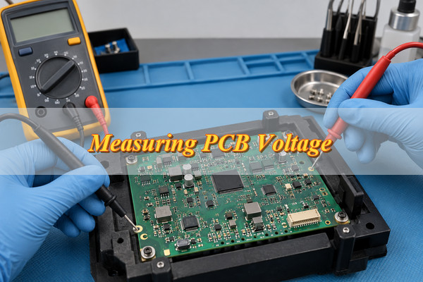
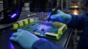
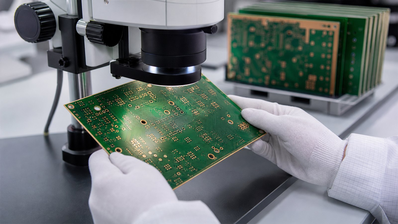
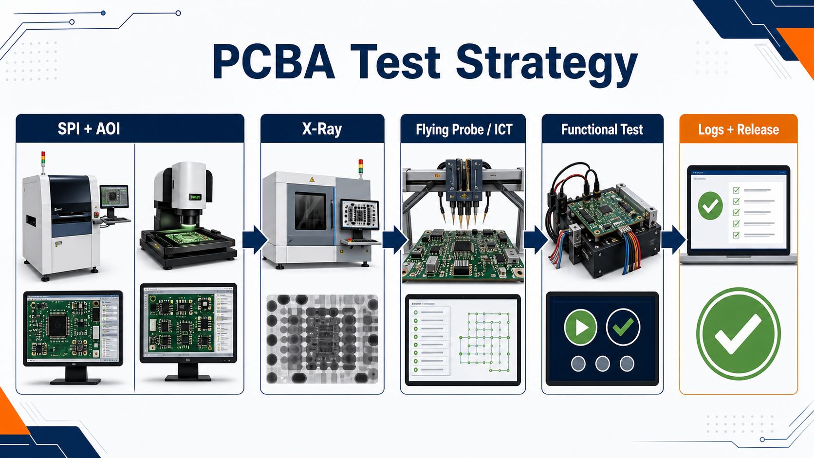
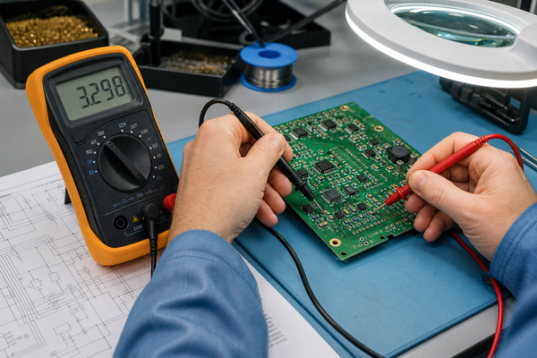
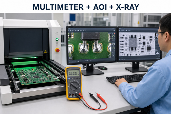
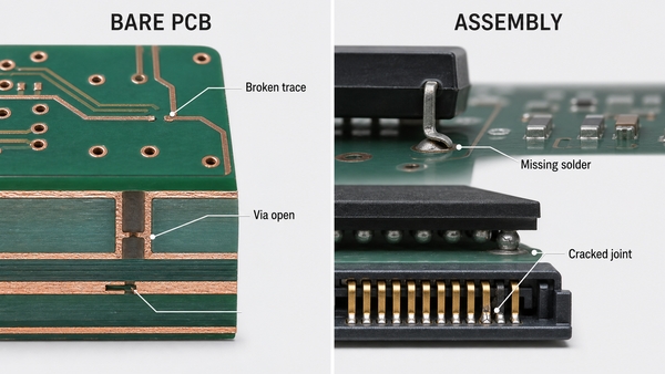
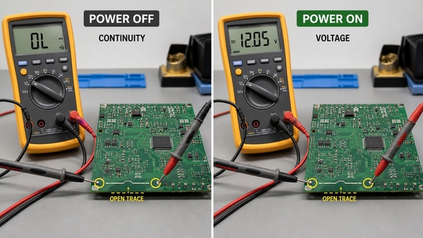
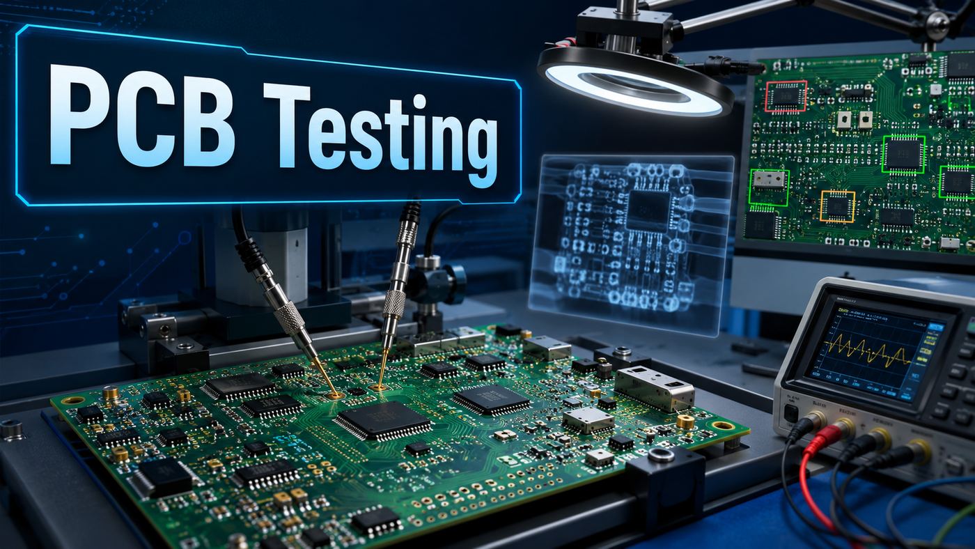
PCB testing workstation with probes, optical inspection, X-ray analysis, and measurement equipment

What Is PCB Testing and What Does It Verify?

PCB testing is the process of finding manufacturing defects and confirming that a circuit board meets its electrical, mechanical, and functional requirements.

The term covers 2 different production stages.

Bare PCB Testing

Bare PCB testing is performed before components are mounted. Its main purpose is to verify the manufactured interconnections against the design netlist.

It can identify:

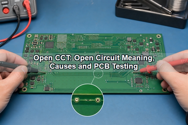
  • Open circuits
  • Short circuits
  • Incorrect net connections
  • Excessive conductor resistance
  • Poor plated-hole continuity
  • Isolation problems between unrelated nets

IPC-9252 provides guidance for selecting test levels, analyzers, test data, parameters, and fixtures for unpopulated printed boards.

However, a bare-board electrical test does not verify component values, solder quality, firmware, or final product operation.

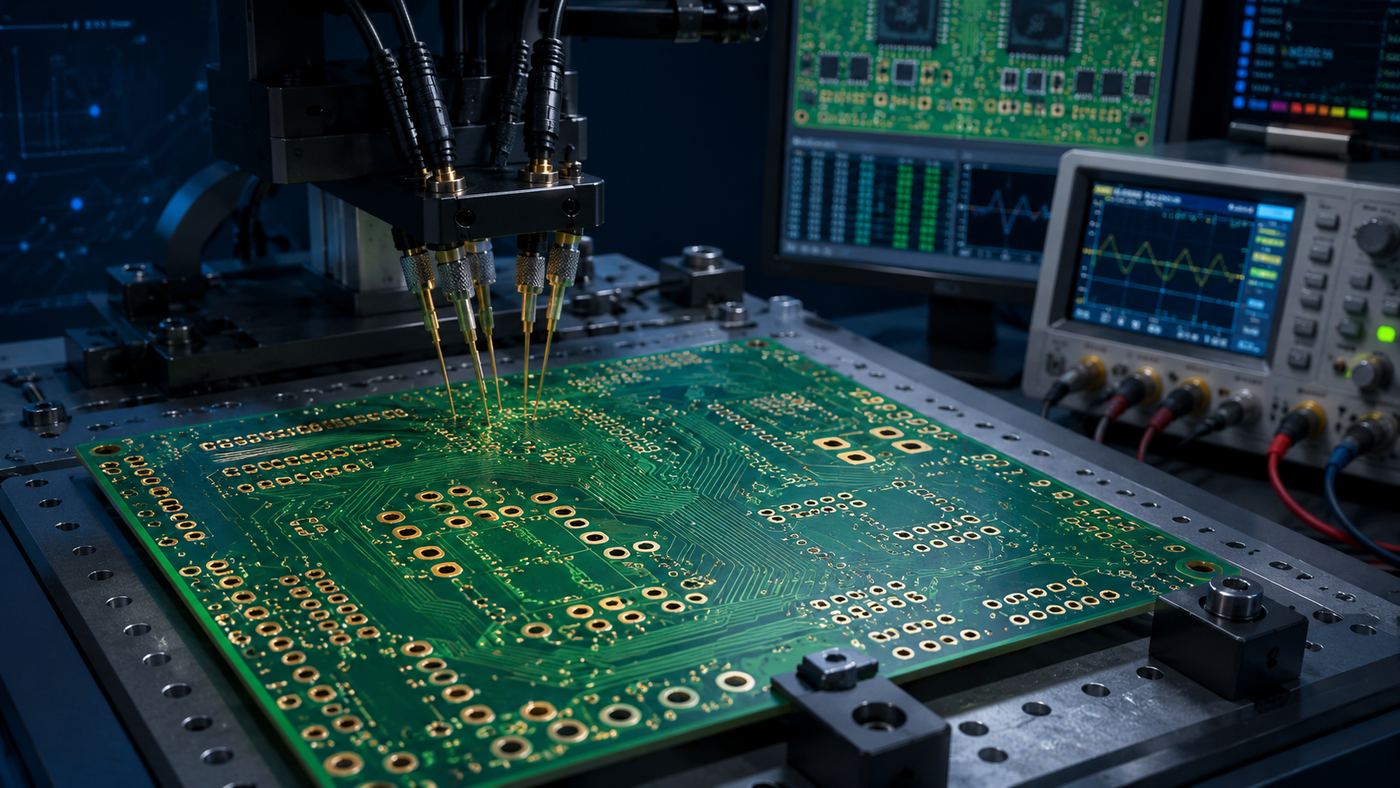
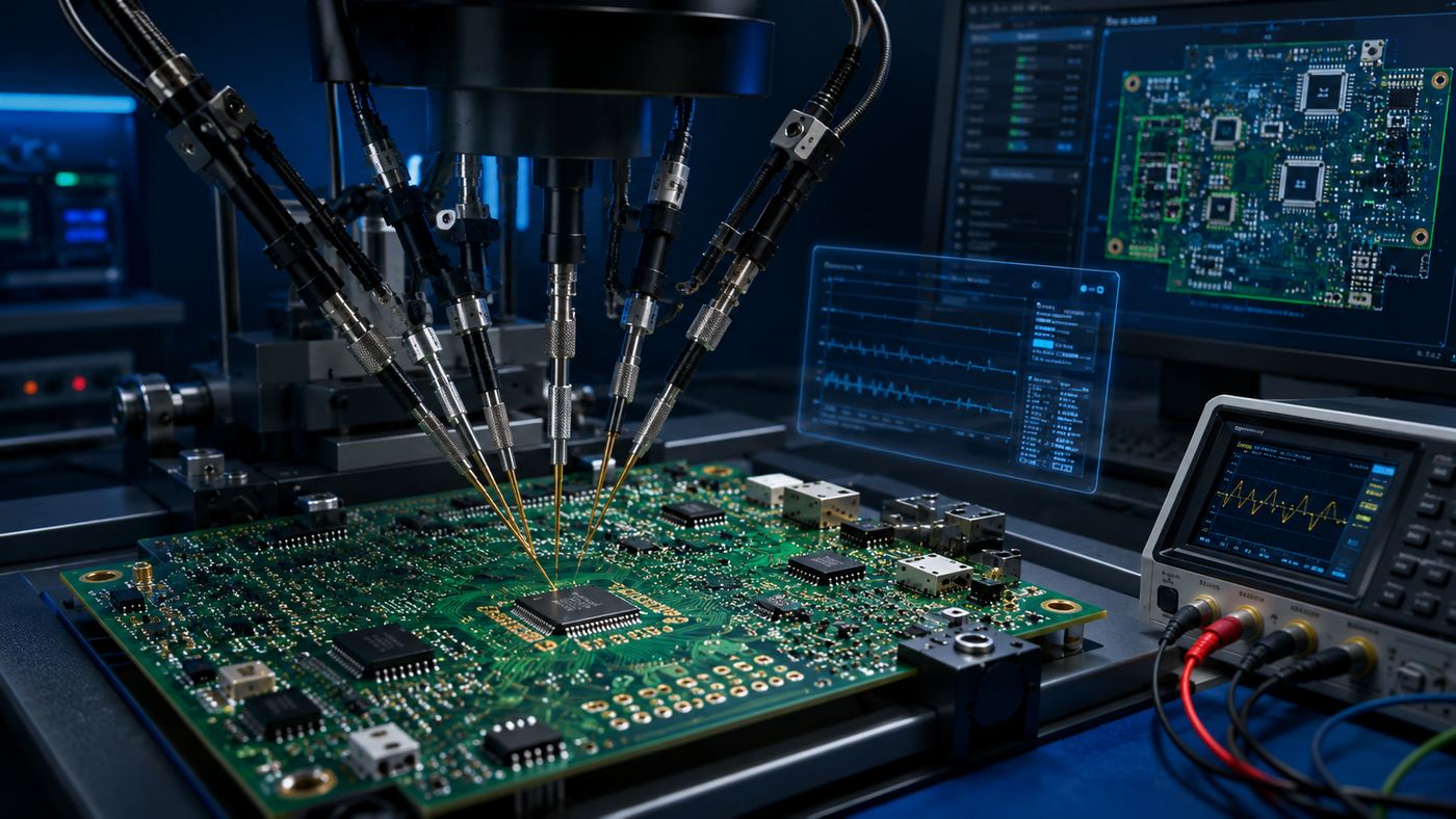
Bare PCB electrical testing with programmable probes checking copper traces, vias, pads, and plated holes

PCBA Testing

PCBA testing is performed after solder paste printing, component placement, reflow, through-hole assembly, or final integration.

It can verify:

  • Solder paste volume and alignment
  • Component presence and orientation
  • Solder-joint quality
  • Resistor, capacitor, diode, and other component values
  • Opens and shorts after assembly
  • Power-rail behavior
  • Communication interfaces
  • Firmware programming
  • Inputs, outputs, sensors, displays, relays, and other functions

The distinction is important. A PCB manufacturer may offer 100% bare-board electrical testing, while PCBA testing may require customer-supplied test procedures, fixtures, firmware, golden samples, or functional limits.

Inspection, Electrical Testing, and Reliability Testing

These terms are related but not interchangeable.

Inspection examines physical workmanship. SPI, AOI, manual inspection, and X-ray belong to this category.

Electrical and functional testing applies measurements or operating conditions to determine whether circuits and components behave correctly. Flying probe, ICT, boundary scan, and FCT belong here.

Reliability testing evaluates whether a design or manufacturing process can survive repeated heat, humidity, vibration, current, or mechanical stress. It is normally used for qualification or sampling rather than as a production test for every board.

A strong test plan uses the right layer of verification at each production stage.

What Is the Standard PCB Testing Procedure?

The exact PCB testing process depends on the product, but a typical manufacturing sequence follows these stages.

Bare-Board Visual and Dimensional Inspection

Before electrical testing, the manufacturer checks:

  • Board dimensions
  • Hole size and location
  • Surface finish
  • Solder mask registration
  • Legend alignment
  • Annular rings
  • Copper exposure
  • Edge damage
  • Bow and twist

Automated optical equipment may support this inspection, but some criteria still require operator review or dimensional measurement.

Bare-Board Electrical Test

The manufactured board is compared with the customer’s netlist or extracted CAD data.

A fixture-based tester or flying probe machine checks continuity within each net and isolation between unrelated nets. High-voltage or low-resistance requirements should be stated in the fabrication drawing or purchase specification rather than assumed.

This step confirms that the copper network is electrically correct before assembly begins.

Solder Paste Inspection

After solder paste printing, SPI measures paste deposits before components are placed.

Typical checks include:

  • Paste height
  • Area
  • Volume
  • Offset
  • Bridging
  • Insufficient paste
  • Excess paste

Catching printing defects at this point is efficient because the board has not yet entered reflow. Paste can often be cleaned and printed again without removing assembled components.

Pre-Reflow and Post-Reflow AOI

Pre-reflow AOI may check component presence, polarity, orientation, and placement offset.

Post-reflow AOI focuses on:

  • Missing components
  • Wrong components
  • Polarity errors
  • Tombstoning
  • Lifted leads
  • Visible solder bridges
  • Insufficient or excessive solder
  • Component displacement

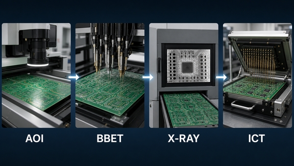
AOI is fast and suitable for inspecting visible features across an SMT production line. Modern inspection systems can measure and classify solder joints, although AOI does not prove that the circuit works electrically.

X-Ray Inspection

X-ray inspection is used where solder joints are hidden beneath a package or cannot be evaluated clearly by optical equipment.

Common applications include:

  • BGA
  • LGA
  • QFN
  • Bottom-terminated components
  • Press-fit connections
  • Through-hole barrel fill
  • Power devices with thermal pads

X-ray can reveal internal voiding, bridges, insufficient solder, head-in-pillow defects, and irregular ball formation. In a coordinated inspection strategy, SPI addresses paste deposition, AOI covers visible assembly features, and X-ray examines internal structures.

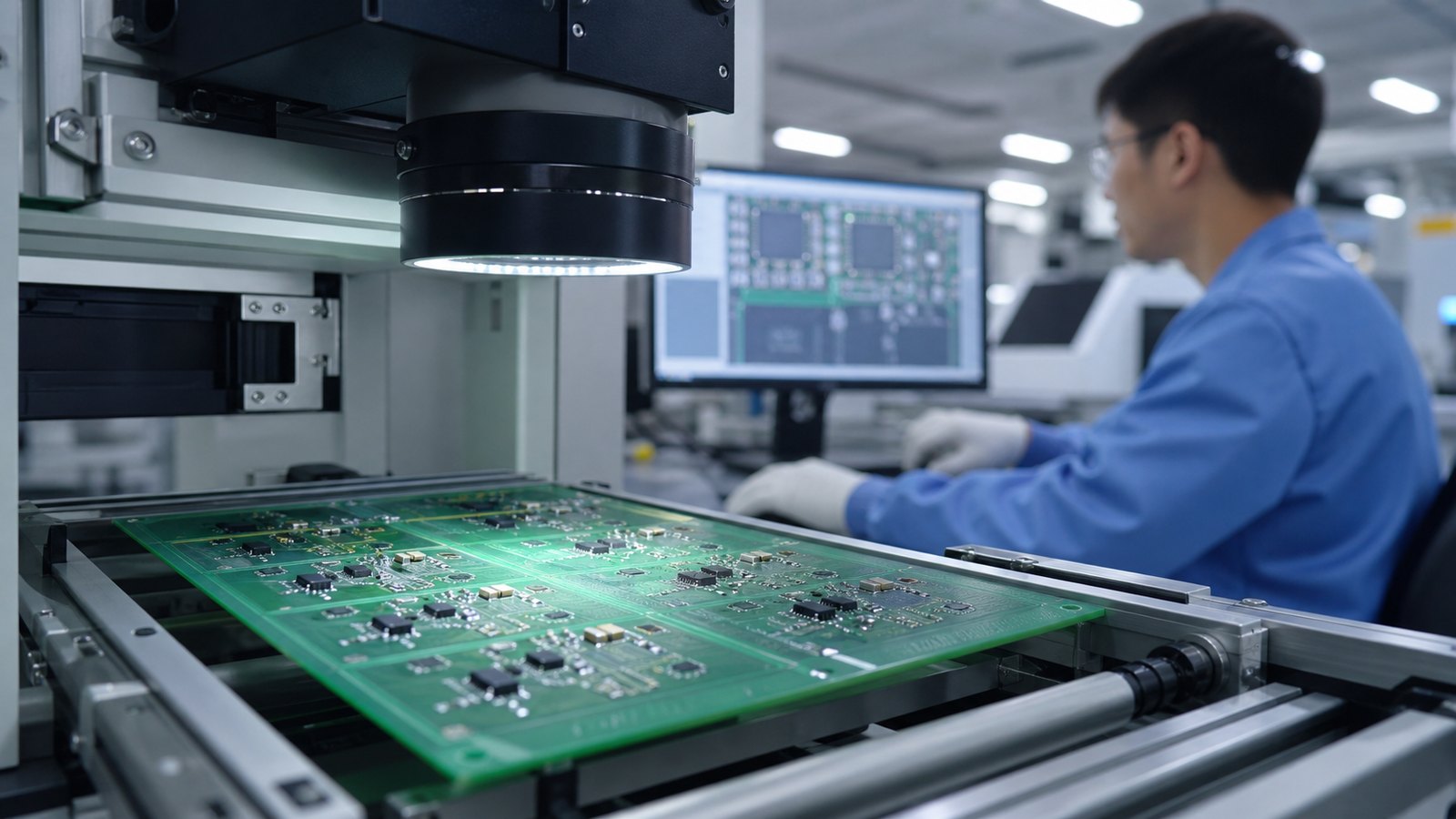
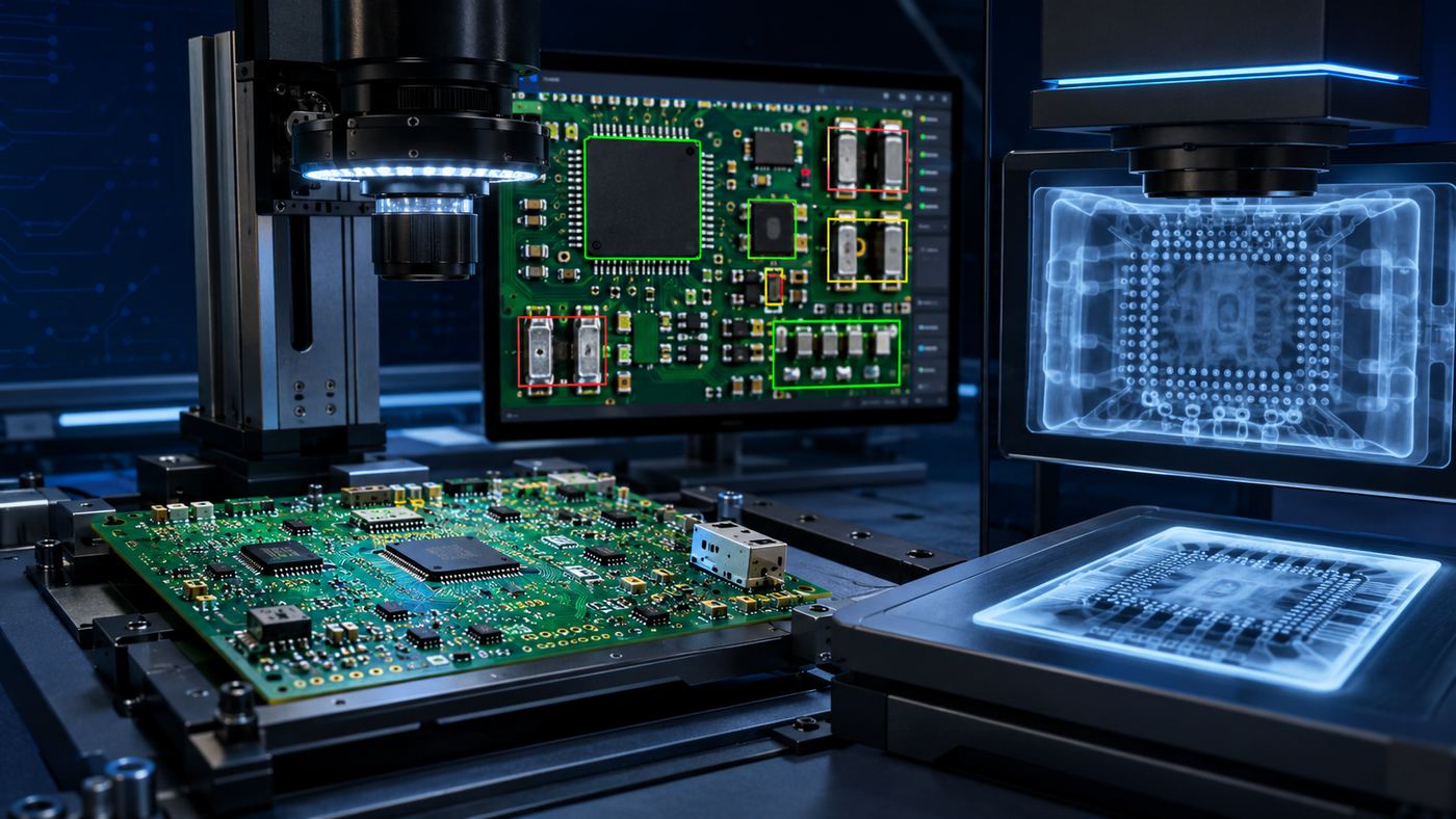
AOI and X-ray inspection of a populated PCB with optical defect overlays and hidden solder-joint imaging

ICT or Flying Probe Testing

After assembly inspection, the board may undergo an electrical structural test.

For prototypes and low-volume orders, flying probe testing is often selected because it does not require a dedicated bed-of-nails fixture.

For stable, higher-volume production, ICT can test many nodes rapidly through a custom fixture. It may check opens, shorts, component values, diode orientation, power rails, and other board-level characteristics.

Firmware Programming

Microcontrollers, FPGAs, EEPROMs, and other programmable devices may be loaded during ICT, functional testing, or a separate programming stage.

The programming process should control:

  • Firmware revision
  • Serial number
  • Configuration data
  • Calibration data
  • Security keys, where applicable
  • Programming verification
  • Traceability records

In-system programming can also be integrated into an ICT platform, reducing separate handling steps.

Functional Circuit Testing

Functional circuit testing powers the PCBA and confirms that it performs its intended operations.

Depending on the product, FCT may measure:

  • Input current
  • Standby current
  • Power-rail voltage
  • Output voltage or current
  • Signal frequency
  • Communication ports
  • Sensor response
  • Motor or relay control
  • Audio, display, LED, or wireless operation
  • Protection and alarm functions

FCT is normally based on the product specification rather than a universal test program.

Reliability Sampling and Final Inspection

High-reliability products may require environmental or endurance testing during qualification, process validation, or lot sampling.

After testing, the manufacturer completes final visual inspection, cleaning verification, labeling, packaging, and test-record review.

The final release decision should be based on defined limits—not an operator’s informal judgment.

What Are the Main PCB Testing Methods?

No test method detects every possible defect. Each one has a distinct role.

Manual Visual Inspection

Manual inspection uses trained operators, magnification equipment, microscopes, and workmanship standards.

It is useful for:

  • Low-volume prototypes
  • Connector inspection
  • Mechanical damage
  • Hand-soldered joints
  • Rework verification
  • Areas that automated equipment cannot view clearly

Its main limitation is consistency. Detection depends on lighting, magnification, operator experience, and inspection time.

Manual inspection works best as a supplement, not the only quality gate.

Solder Paste Inspection

SPI is performed immediately after solder paste printing.

It is particularly valuable for fine-pitch components because paste volume directly affects the joint formed during reflow. Too little paste can produce opens or weak joints, while excessive or misaligned paste may create bridging.

SPI does not inspect the final solder joint. It controls the process before the joint is created.

Automated Optical Inspection

AOI captures images of the assembly and compares measured features with programmed rules, CAD data, or reference models.

Its strengths include:

  • High inspection speed
  • Repeatable coverage
  • Early process feedback
  • Automated defect classification
  • Support for statistical process control

AOI is highly effective for visible defects but has limited access beneath BGA, LGA, QFN, and other bottom-terminated packages.

It also cannot confirm that a correctly oriented component has the correct internal value or that firmware is functioning.

Automated X-Ray Inspection

AXI uses X-rays to examine solder joints and conductive structures beneath components.

It is suitable for dense boards with:

  • BGAs
  • Area-array packages
  • Hidden thermal pads
  • Double-sided assemblies
  • Complex through-hole joints
  • High-reliability solder requirements

X-ray inspection provides structural evidence, but it does not replace electrical or functional testing. A solder joint may look acceptable while the circuit contains a wrong-value component or defective IC.

Bare PCB Electrical Testing

Bare-board electrical testing checks the manufactured copper network before assembly.

Two common approaches are used:

Fixture testing contacts many test points simultaneously through a dedicated fixture. It offers fast cycle times for repeated production.

Flying probe testing moves independent probes between pads, vias, and test points. It reduces tooling requirements and adapts more easily to revision changes.

The test data should be generated from controlled Gerber, ODB++, IPC-2581, netlist, or original CAD information. Testing against the wrong revision can produce a valid report for the wrong board.

Flying Probe Testing

Flying probe testing uses programmable moving probes instead of a fixed bed-of-nails fixture.

It is well suited to:

  • Engineering samples
  • PCB prototypes
  • Small batches
  • Frequent design revisions
  • Products with limited fixture budget
  • New product introduction

Its main advantage is flexibility. Changes can often be handled by updating the test program rather than rebuilding a fixture.

The trade-off is test time. Probes contact test points sequentially, so a complex board may take longer than ICT.

Flying probe is not automatically superior for every prototype. Probe access, component density, board size, test coverage, and required measurements still affect feasibility.

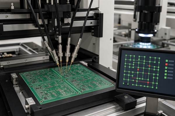
Flying probe PCB testing machine using multiple programmable probes on a prototype circuit board

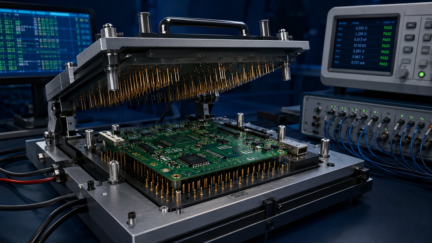
In-Circuit Testing

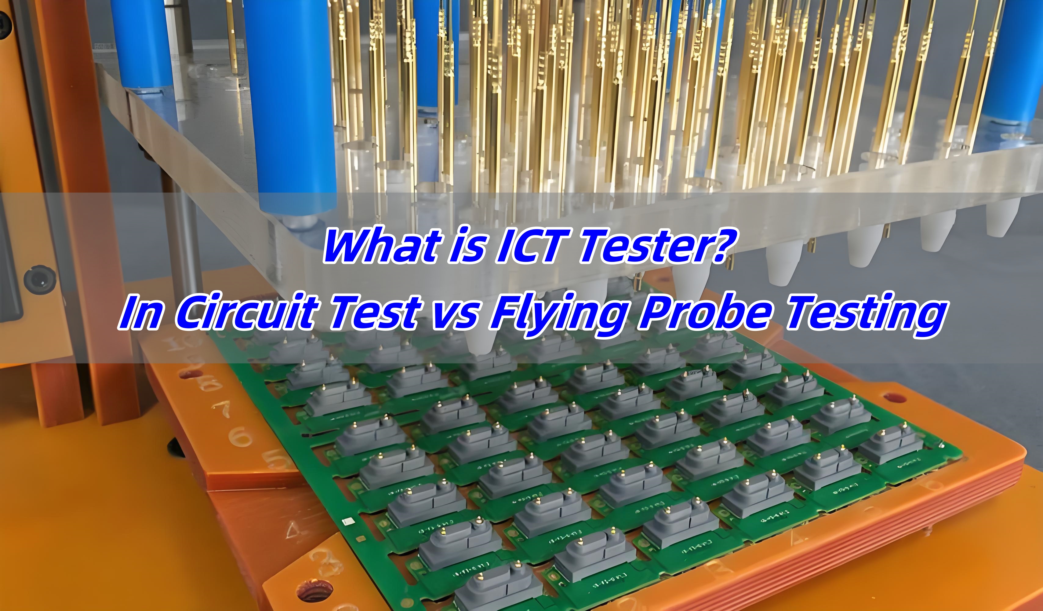
ICT uses electrical access to individual circuit nodes, commonly through a bed-of-nails fixture.

It can detect:

  • Assembly opens and shorts
  • Missing components
  • Incorrect component values
  • Reversed diodes
  • Some incorrect IC placements
  • Power-rail faults
  • Certain soldering defects

ICT offers fast component-level fault isolation and is particularly effective in stable, higher-volume manufacturing. Complementary technologies such as boundary scan can extend coverage on dense boards.

The primary constraints are fixture cost, test-point access, program development, and maintenance after PCB revisions.

In-circuit testing fixture with a populated PCBA, bed-of-nails pogo pins, and automated pass-fail instrumentation

Boundary Scan Testing

Boundary scan uses test circuitry built into compatible ICs and is commonly associated with JTAG or IEEE 1149.x devices.

It can help test connections between digital devices where physical probes cannot reach every net.

Applications include:

  • Dense BGA assemblies
  • Processor and FPGA boards
  • Digital interconnect verification
  • Flash programming
  • Limited-access designs

Boundary scan requires compatible components and correct scan-chain implementation. It does not provide full coverage for analog circuits or devices without boundary scan support.

It is often integrated with ICT rather than used as a complete replacement.

Functional Circuit Testing

FCT verifies the assembled board in an operating or simulated operating condition.

Unlike ICT, which focuses heavily on component-level faults, FCT asks a broader question: does the board perform its intended job?

A functional test may include:

  • Power-up sequencing
  • Current-consumption limits
  • Analog input and output checks
  • Digital I/O
  • Communication protocols
  • User controls
  • Displays and indicators
  • Load simulation
  • Safety interlocks
  • Calibration

FCT may identify that the board fails, but it may not isolate the exact defective component as quickly as ICT.

For this reason, ICT and FCT are often complementary. ICT supports diagnosis; FCT confirms system behavior.

Burn-In and Reliability Testing

Burn-in operates the PCBA for an extended period, sometimes under elevated temperature, repeated power cycling, or electrical load.

It may help expose early-life failures related to:

  • Marginal components
  • Poor solder joints
  • Thermal instability
  • Intermittent connections
  • Power-device weakness

Burn-in is not needed for every consumer product. It is more appropriate when field failure carries a high cost or the product specification explicitly requires endurance screening.

What Equipment, Jigs, and Software Are Used for PCB Testing?

PCB testing equipment includes more than a single PCB testing machine. Fixtures, instruments, software, data limits, and traceability all affect the result.

Test equipment Main purpose Typical production stage
Bare-board electrical tester Opens, shorts, continuity, isolation PCB fabrication
Flying probe tester Fixtureless electrical measurements Prototype or low-volume PCB/PCBA
SPI machine Solder paste height, area, volume, offset After printing
AOI machine Visible component and solder defects Before or after reflow
X-ray or AXI system Hidden solder-joint inspection After reflow
ICT system Component-level electrical checks PCBA production
Functional test jig Product-specific operating test Final PCBA stage
Oscilloscope Waveform, timing, ripple, frequency Debugging or FCT
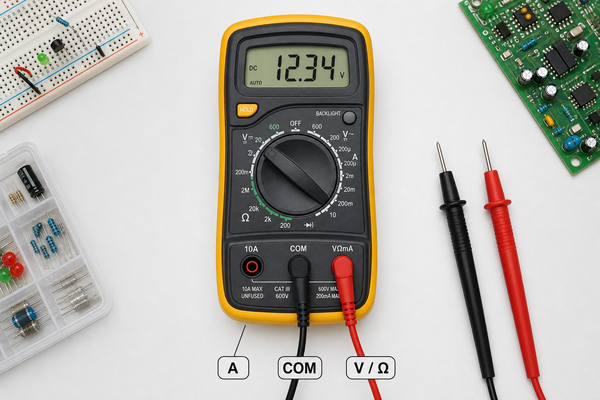
DMM Voltage, current, resistance, continuity ICT, FCT, repair
Programmable power supply Controlled board power and protection FCT
Electronic load Output loading and regulation tests Power electronics
DAQ and switching system Multi-channel automated measurements Automated FCT

PCB Testing Jigs

A test jig provides mechanical alignment and electrical connection between the test equipment and the board.

It may include:

  • Pogo pins
  • Connectors
  • Pneumatic or manual clamping
  • Relay switching
  • Power supplies
  • Loads
  • Sensors
  • Safety covers
  • Barcode readers
  • Status indicators
  • Replaceable wear parts

A reliable jig must contact the board without damaging pads, bending the PCB, or creating unstable readings.

PCB Testing Software

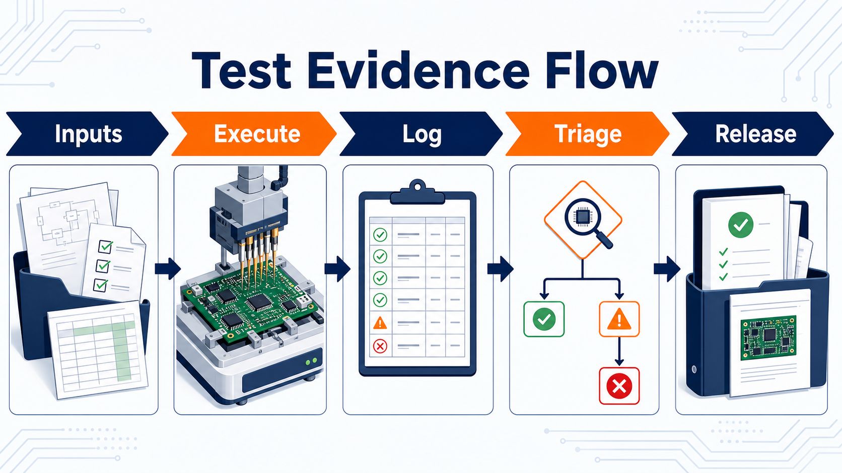
Test software controls instruments, applies limits, records measurements, and generates pass/fail results.

A practical software architecture may include:

  • Test-sequence control
  • Instrument drivers
  • Fixture control
  • Firmware programming
  • Limit files
  • User permissions
  • Error handling
  • Serial-number tracking
  • Data export
  • MES integration

The software should store actual measurements where useful. A simple “PASS” record provides less diagnostic value than a report showing measured voltage, expected limits, test time, and failure location.

How Do You Choose the Right PCB Testing Method?

The best method depends on product risk, board design, production volume, and fault coverage.

Method Fixture required Relative test speed Best use Main limitation
Visual inspection No Medium Prototypes and workmanship checks Operator-dependent
SPI No product fixture Fast SMT paste-process control Only checks printed paste
AOI No electrical fixture Fast Visible SMT defects Cannot inspect hidden joints or prove function
X-ray No contact fixture Medium BGA, QFN, hidden joints Structural inspection only
Flying probe Usually no dedicated fixture Slow to medium Prototype and low-volume production Longer cycle time
ICT Yes Very fast Stable medium- or high-volume PCBA Fixture cost and test-point demand
Boundary scan No bed-of-nails fixture required Fast Dense digital boards Requires compatible devices and design support
FCT Usually yes Application-dependent Final product behavior Program and fixture development
Reliability testing Test coupons or chambers Slow Qualification and process validation Not a routine per-board test

For Prototypes

A practical PCB prototype test plan often includes:

  • 100% bare-board electrical testing
  • SPI and AOI during SMT assembly
  • X-ray for BGA or hidden-joint packages
  • Flying probe when electrical access allows it
  • Basic power-up and functional verification
  • Detailed engineering inspection of the first article

A costly ICT fixture may not be economical when the layout is still changing.

For Small-Batch Production

Small-batch products benefit from flexible methods:

  • Flying probe
  • Reusable connector-based functional jigs
  • Modular DAQ systems
  • Firmware programming
  • AOI and targeted X-ray
  • Golden-sample comparison

The goal is to gain useful coverage without excessive non-recurring engineering cost.

For Mass Production

Stable, high-volume products may justify:

  • Dedicated ICT fixtures
  • Automated board handling
  • Inline AOI or AXI
  • Automated firmware programming
  • Parallel functional testing
  • Barcode tracking
  • MES data collection
  • Statistical analysis of repeated failures

ICT has higher initial preparation costs, but its simultaneous fixture access can provide much faster throughput than sequential flying probes in volume production.

For High-Reliability Products

Automotive, medical, aerospace, industrial control, and power electronics may need a deeper strategy based on the product’s actual risk.

Possible additions include:

  • Extended FCT
  • High-voltage testing
  • Leakage-current testing
  • Boundary scan
  • Thermal cycling
  • Burn-in
  • Vibration testing
  • Conformal-coating inspection
  • Lot traceability
  • Calibration records
  • Failure-analysis procedures

Industry certification alone does not define the product test. The drawing, quality plan, acceptance criteria, and customer specification must identify what is required.

How Does Design for Testability Improve PCB Test Coverage?

Design for testability, or DFT, makes the board easier to inspect, probe, program, diagnose, and verify.

It should begin during schematic and PCB layout—not after the production fixture has been ordered.

Add Accessible Test Points

Important nets may need test access, including:

  • Ground
  • Main input power
  • Regulated power rails
  • Reset
  • Clock
  • Communication buses
  • Programming signals
  • Critical analog signals
  • Safety-monitoring signals

Test points should have enough diameter and clearance for the selected probe system.

Avoid Probe Collisions

Probe access can be blocked by:

  • Tall components
  • Connectors
  • Shielding cans
  • Heat sinks
  • Board edges
  • Closely spaced test points
  • Components on the opposite side of a thin PCB

The fixture designer should review the final mechanical arrangement, not only the electrical netlist.

Plan Power Isolation

Some circuits need resistors, jumpers, relays, or removable links so individual power sections can be tested safely.

Without isolation, a short or wrong component in one section may affect measurements across several rails and make fault diagnosis difficult.

Provide a Stable Programming Interface

Programming pads or connectors should expose the required:

  • Data
  • Clock
  • Reset
  • Power
  • Ground
  • Boot-mode signals

The board should also provide a reliable method for confirming the programmed firmware version.

Consider Boundary Scan Early

Boundary scan must be supported by the chosen components and connected correctly in the schematic.

The scan chain, pull resistors, connectors, device order, and boot behavior should be reviewed before layout release.

Control Test Documentation

The manufacturer may need:

  • Gerber or ODB++ data
  • BOM
  • Pick-and-place file
  • Schematic
  • Netlist
  • Test-point list
  • Firmware
  • Programming instructions
  • Test procedure
  • Expected limits
  • Connector pinout
  • Golden sample
  • Failure examples

Providing only a finished PCB layout is rarely enough to develop a comprehensive PCBA functional test.

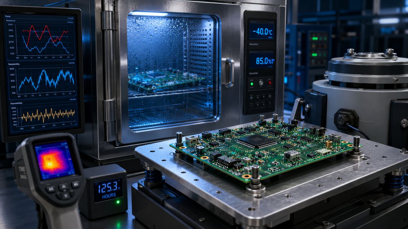
When Is PCB Reliability or Environmental Testing Required?

PCB environmental testing examines whether the board, materials, interconnections, and assembly process can survive expected service conditions.

It may be required when:

  • The product operates at high or low temperature
  • Temperature changes are frequent
  • The assembly experiences vibration or shock
  • Humidity or condensation is possible
  • High current flows through vias or plated holes
  • The board contains HDI microvias
  • Field access is difficult
  • Failure creates safety or financial risk
  • A customer or regulatory plan specifies qualification tests
PCB environmental and reliability testing with a temperature-humidity chamber, vibration platform, and thermal monitoring

Interconnect Stress Testing

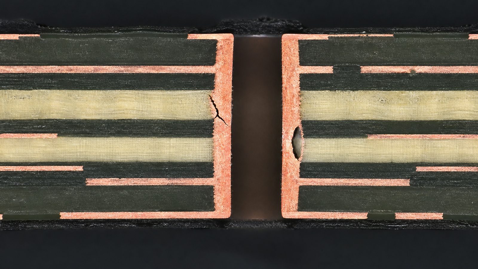
IST evaluates the durability of plated through-holes, vias, and other interconnect structures by cycling the test coupon through controlled heating and cooling.

The method uses DC current to resistance-heat the interconnect structure, creating repeated thermal excursions and thermo-mechanical fatigue.

IST is especially useful when assessing multilayer constructions, plated-hole quality, HDI structures, or process changes.

Thermal Cycling and Thermal Shock

Thermal cycling gradually moves the sample between temperature extremes. Thermal shock uses more abrupt transitions.

These tests can expose:

  • Barrel cracking
  • Pad lifting
  • Microvia separation
  • Laminate stress
  • Solder fatigue
  • Component and PCB expansion mismatch

Test temperature, dwell time, ramp rate, cycle count, sample size, and failure criteria should come from the product qualification plan.

Temperature and Humidity Testing

Humidity testing evaluates insulation, corrosion resistance, contamination, and moisture-related degradation.

It may be combined with electrical bias when the objective is to study leakage paths, electrochemical migration, or insulation resistance.

Vibration and Mechanical Shock

Vibration and shock testing are relevant to vehicles, industrial machinery, aircraft, handheld equipment, and products shipped in demanding conditions.

The test fixture should reproduce the intended mounting points. Supporting the sample incorrectly may create a failure mode that would not occur in the actual enclosure.

CAF and SIR Testing

Conductive anodic filament testing evaluates electrochemical growth through laminate material between conductors.

Surface insulation resistance testing evaluates electrical resistance across a contaminated or moisture-exposed surface.

These methods are normally used for material, process, cleanliness, or reliability qualification rather than routine PCB board testing.

Third-Party PCB Testing Laboratories

A third-party laboratory may be appropriate when the project requires:

  • Independent qualification
  • Specialized environmental chambers
  • Failure analysis
  • Microsection evaluation
  • Ionic contamination testing
  • Material verification
  • Regulatory documentation
  • Customer-witnessed testing

Before ordering laboratory work, define the test method, sample condition, preparation method, acceptance limit, reporting format, and handling of failed samples.

What Should Be Included in a PCB Testing Report?

A useful PCB testing report must connect the result to the correct product, revision, process, and test program.

It should include:

  • Customer or project name
  • PCB or PCBA part number
  • Board revision
  • Manufacturing lot
  • Serial number, where applicable
  • Test date and time
  • Test-station identification
  • Fixture revision
  • Software or program revision
  • Firmware version
  • Test method
  • Measured values
  • Upper and lower limits
  • Pass/fail result
  • Failed net, component, or test step
  • Operator or system identification
  • Retest status
  • Repair or rework record

For prototype debugging, waveform captures, X-ray images, AOI defect images, and failed measurements can be more useful than a simple pass/fail certificate.

The report format should be agreed before production. Reconstructing missing traceability after shipment is far harder than recording it during the test.

How Does EBest Circuit Test PCB and PCBA Orders?

EBest Circuit builds the test plan around the manufacturing stage, product complexity, production quantity, and customer requirements.

Available quality-control and testing support can include:

  • Bare-board electrical testing
  • Solder paste inspection
  • Automated optical inspection
  • X-ray inspection
  • Flying probe testing
  • ICT fixture coordination
  • Firmware programming
  • Functional test jig development
  • Functional circuit testing
  • Test-report preparation
  • MES and lot traceability
  • Reliability testing based on project requirements

For PCBA functional testing, customers should provide the schematic, product specification, firmware, interface definitions, expected measurements, pass/fail limits, and a working golden sample where available.

Providing this information during quotation allows the engineering team to evaluate fixture cost, test coverage, cycle time, programming needs, and equipment requirements before production begins.

For PCB fabrication, turnkey PCBA, or a project-specific PCB testing procedure, contact sales@bestpcbs.com for a DFM and testability review.

Frequently Asked Questions About PCB Testing

1. What is the most common PCB testing method?

For bare PCBs, electrical continuity and isolation testing are common production checks. For assembled PCBAs, AOI is widely used after reflow, often combined with X-ray, flying probe, ICT, or functional testing depending on the board.

There is no single test that covers every defect.

2. What is the difference between PCB testing and PCBA testing?

PCB testing normally refers to an unpopulated board and focuses on copper connections, opens, shorts, and isolation.

PCBA testing is performed after components are installed. It may check soldering, component values, firmware, power rails, interfaces, and complete circuit operation.

3. Is flying probe testing better than ICT for prototypes?

Flying probe is usually more practical for prototypes because it does not require an expensive dedicated bed-of-nails fixture and can accommodate design revisions more easily.

ICT becomes more attractive when the design is stable and production volume is high enough to justify fixture development.

4. Can AOI detect electrical faults on a PCB?

AOI can detect many visible assembly defects, such as missing components, polarity errors, shifted parts, and some solder problems.

It cannot directly prove continuity, component value, firmware operation, or circuit function. Electrical testing is still needed for those checks.

5. What does a PCB functional test check?

A PCB functional test powers the assembly and checks whether it operates according to the product specification.

It may measure current, voltages, signals, communications, sensors, outputs, displays, switches, relays, or protection functions.

6. Does every PCB need environmental reliability testing?

No. Routine commercial boards may not need full thermal, humidity, vibration, or burn-in qualification.

These tests are more relevant when required by the application, customer specification, qualification plan, safety risk, or expected operating environment.

7. What files are required to develop a PCB testing jig?

The exact package depends on the test, but it often includes:

  • Gerber or ODB++ files
  • Schematic
  • BOM
  • Pick-and-place data
  • Test-point list
  • Mechanical drawing
  • Connector definition
  • Firmware
  • Programming instructions
  • Functional test procedure
  • Expected limits
  • Golden sample

Complete and revision-controlled data reduces fixture rework and improves test coverage.

Ready to Define the Right PCB Testing Plan?

Match the test strategy to the board stage, product risk, production volume, and required fault coverage. For a project-specific review, send EBest Circuit the Gerber data, BOM, schematic, quantities, test limits, firmware, and available golden sample.

You may also like

PCB Bare Board Testing: Methods, Standards, Reports & Acceptance Criteria
Monday, July 20th, 2026

PCB bare board testing verifies opens and shorts before assembly. It compares the electrical networks of an unpopulated printed circuit board with approved connectivity data before defects become harder and more expensive to isolate. A meaningful result must also identify the tested revision, coverage, limits, exclusions, traceability, and disposition rules.

A “passed” label is meaningful only when the method, source netlist, limits, exclusions, and report content are defined. Electrical verification does not replace visual, dimensional, impedance, cleanliness, solderability, or reliability controls.

Flying probes performing PCB bare board testing on an unpopulated circuit board

What Is PCB Bare Board Testing?

PCB bare board testing verifies continuity and isolation. Continuity testing and isolation testing compare accessible conductive points with a reference derived from the released design. Net count, board density, via structures, access constraints, and special measurements determine test complexity.

The test is often called bare-board electrical test, E-test, continuity-and-isolation test, or netlist test. It can identify electrical opens and shorts, but it does not prove that every physical feature meets drawing requirements. It also does not guarantee that an assembled product will function. Visual workmanship, dimensions, copper and plating requirements, controlled impedance, solderability, cleanliness, and assembly performance remain separate verification activities.

Why Is Bare Board Testing Important Before PCB Assembly?

PCB bare board testing prevents known defects from entering assembly. Its value can be divided into four practical benefits:

  • Lower assembly loss: Detecting opens and shorts before component placement avoids wasting components, reflow capacity, inspection time, and troubleshooting labor.
  • Earlier defect containment: Testing close to PCB fabrication allows affected boards to be isolated before more value is added. This is especially useful for fine-pitch parts, buried connections, dense multilayers, and products that are difficult to probe after assembly.
  • Clear responsibility boundary: The PCB manufacturer can document the electrical condition at shipment, while the assembler controls handling, storage, assembly, and downstream testing.
  • Better purchase-order control: Defined coverage reduces disputes caused by vague language such as “electrically tested.” The order should identify the data revision, coverage level, acceptance basis, reporting needs, and special test conditions.

What Defects Can Bare Board Testing Detect?

PCB bare board testing finds electrical connectivity defects. The main results depend on test access, the approved program, and the specified measurement conditions:

  • Open circuits: PCB bare board testing detects interrupted nets caused by incomplete etching, cracked copper, failed via connections, annular-ring breakout, poor hole-wall metallization, or routing damage.
  • Short circuits: It detects unintended connections caused by copper bridges, conductive residue, imaging errors, plating anomalies, or incorrect fabrication data.
  • Intermittent connections: Unstable defects may require repeated measurements, thermal conditioning, resistance monitoring, microsectioning, or reliability testing.
  • Not covered by electrical testing: Visual defects, dimensional errors, impedance deviations, contamination, solder-mask registration, and material conditions require separate inspection or measurement.

Flying Probe vs Fixture Testing: Which Bare Board Testing Method Should You Choose?

For PCB bare board testing, use flying probe testing for flexibility. Use fixture testing for throughput. The final choice depends on volume, revision stability, access, setup cost, and required test time.

Decision Factor Flying Probe Fixture Testing
Operating principle Moving probes contact test points sequentially according to the test program A dedicated adapter contacts many test points in parallel
Typical fit Prototype, low volume, frequent revision Stable design, medium-to-high volume
Dedicated tooling Usually not required Required and revision-specific
Setup profile Program generation and validation Fixture plus program generation and validation
Throughput Sequential probing; often slower Parallel contact; often faster after setup
Upfront cost Lower because no dedicated fixture is normally needed Higher because the fixture must be designed, built, and validated
Cost per board Can remain higher as test time increases with point count Can decrease across stable production volumes after setup
Revision response Program changes may be sufficient Fixture rework or replacement may be needed
Access risk Probe reach, pad size, stability, and routing Probe density, fixture mechanics, alignment, and wear
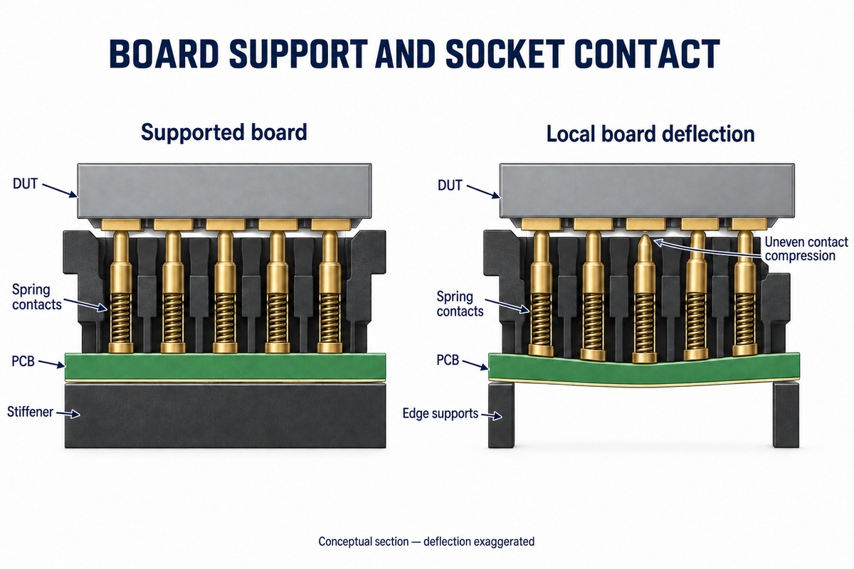
Board support Requires stable positioning during probe movement Requires uniform support and controlled pressure across the fixture
Maintenance Probe condition, alignment, and program control Probe wear, fixture cleaning, storage, alignment, and revision control
Special measurements Flexible for selected points, low-resistance checks, or engineering investigation when equipment supports them Suitable for repeatable production measurements when designed into the fixture and switching system
Primary limitation Runtime increases with test-point count and measurement scope Tooling cost and lead time are difficult to justify for changing designs
Best selection rule Choose when flexibility and low setup commitment outweigh runtime Choose when stable volume and throughput justify dedicated tooling
Bare PCB positioned on a dedicated bed-of-nails electrical test fixture

Which Board and Order Factors Affect Test-Method Selection?

Balance coverage risk, design stability, setup cost, and runtime. Review production quantity, expected repeat orders, board size, net and test-point count, pad geometry, layer count, via technology, panel format, and required measurements. A prototype likely to change favors flexible programming; a mature design produced repeatedly may justify a fixture whose preparation cost is distributed across more units.

Then examine what must be tested and what is physically accessible. Fine-pitch pads, solder-mask clearance, surface finish, board support, bow and twist, and probe force can affect contact reliability. Controlled-impedance verification, very low resistance, or elevated-voltage isolation may require methods beyond a basic continuity-and-isolation routine. The manufacturer should review unusual requirements before quotation so the chosen method, limits, tooling, report, and lead time are aligned.



How Does the PCB Bare Board Testing Process Work?

PCB bare board testing starts with controlled data. Confirm the released revision, reference netlist, accessible points, and approved limits before loading the board. The following eight steps create a traceable test and release process.

  1. Review the order and data package. Confirm part number, revision, quantity, panelization, applicable drawings, test coverage, special nets, reporting, and acceptance requirements.
  2. Create and compare the test reference. Generate connectivity from trusted design data and perform an independent comparison where required to reduce the risk of testing a fabrication error against the same erroneous source.
  3. Prepare the program and access plan. Map test points, choose probe paths or fixture contacts, apply agreed limits, and identify intentionally untested or inaccessible points.
  4. Validate setup. Check alignment, contact, board support, program revision, fixture identification, and known-reference behavior before production testing.
  5. Run continuity and isolation checks. Test the required networks and capture failures with sufficient location information for diagnosis.
  6. Confirm suspect results. Clean or inspect contact surfaces, repeat the measurement under controlled rules, and distinguish contact instability from a repeatable board defect.
  7. Control nonconforming boards. Segregate failures, record disposition, control any repair or retest authorization, and preserve traceability.
  8. Release records. Link the test status and report to the correct lot, date, equipment or program, and approved product revision.

Which Standards Apply to PCB Bare Board Testing?

PCB bare board testing standards must be named by revision. IPC-9252B addresses test data, parameters, equipment, and fixturing for unpopulated boards. IPC’s current revision table marks IPC-9252 as no longer maintained. The purchase order should therefore identify the accepted revision or an agreed alternative. Its scope is conductive-network verification, not every physical, material, dimensional, or assembly requirement.

IPC-A-600 addresses externally and internally observable acceptability conditions; IPC’s revision table listed IPC-A-600M in May 2025. The applicable IPC-6010-series performance specification and procurement documentation define requirements for the relevant board type and class. Drawings, purchase orders, approved deviations, and sector-specific requirements may add controls, so the contract should state document revisions and order of precedence.

High-voltage, aerospace, medical, automotive, or other high-reliability applications may demand additional validation, records, or process controls. Those requirements should be specified by the responsible design authority. A supplier should not infer a hipot voltage, insulation criterion, test class, or sampling permission from the product description alone.

What Files Are Needed for PCB Bare Board Testing?

The test package must identify the product and test reference. Provide the following controlled files and instructions:

  • Fabrication data: Supply the released Gerber or ODB++ package with clear layer identification.
  • Drill data: Include plated and non-plated drill files plus any required drill drawing or tool information.
  • Product identification: State the part number, fabrication revision, board or panel drawing, quantity, and panelization requirements.
  • Reference netlist: Provide IPC-D-356 or trusted CAD-derived connectivity data when an independent electrical reference is required. If the netlist is extracted from fabrication files, define how it is generated and compared.
  • Test requirements: Define coverage, continuity and isolation limits, inaccessible points, no-probe areas, and any special measurement conditions.
  • Special structures: Identify net ties, intentionally connected planes, embedded components, isolated copper, edge contacts, castellations, coupons, and controlled-impedance requirements.
  • Reporting instructions: Specify lot- or serial-level reporting and whether the deliverable must include a certificate, summary, raw measurements, or failure map.
  • Data-control rules: Define secure transfer, authorized access, retention, and deletion requirements for commercially sensitive design files.

100% Netlist Testing vs Optimized Testing vs Sampling

These three coverage models are not interchangeable. The order must define the tested units, program scope, exclusions, and approval basis rather than relying on a short coverage label.

Coverage Model Meaning to Confirm Procurement Control
100% netlist test Every production board runs the defined electrical program; this does not mean every physical feature is measured Define accessible nodes, program scope, exclusions, and lot traceability
Optimized test The program reduces redundant contacts or sequences while preserving the agreed network verification Approve the optimization basis, retained coverage, and excluded points
Sampling Only units selected by the approved sampling plan are tested; other boards remain untested State the sample size, selection method, acceptance rule, risk basis, and authorization

Sampling must not replace contracted every-board testing. Any change requires written authorization under the applicable specification and risk assessment.

What Are the Acceptance Criteria for Bare PCB Testing?

Acceptance criteria must turn “pass” into measurable rules. Define the following items before program approval and production testing:

  • Continuity limit: State the maximum permitted resistance for an intended net, using values appropriate to trace length, conductor geometry, connectors, planes, and low-resistance paths.
  • Isolation limit: Define the minimum resistance or maximum leakage allowed between separate nets. High-voltage products may require different limits and test conditions from routine circuitry.
  • Coverage: Specify whether every board, an optimized net set, or an approved sample is tested. Identify inaccessible points, excluded features, and permitted optimization.
  • Special measurements: For hipot, four-wire resistance, or other special checks, define voltage, current, dwell time, temperature, measurement method, test location, and guarding requirements.
  • Data identity: Link acceptance to the correct part number, fabrication revision, controlled netlist or checksum, test-program revision, and approved change record.
  • Failure confirmation: Define how contact instability is distinguished from a repeatable board defect and which controlled measurements may be repeated.
  • Repair and retest: State whether repair is permitted, who can authorize it, which workmanship rules apply, and whether the affected net or complete program must be rerun.
  • Required evidence: Define the certificate, test summary, failure map, raw results, traceability fields, and record-retention period required for acceptance.

Do not apply one generic limit to every design. Electrical limits must follow the product’s design intent, governing specification, and confirmed test feasibility.

What Should a Bare Board Test Report Include?

A useful report must link results to the delivered boards. Specify the required report level in the purchase order:

  • Product identity: Customer part number, fabrication revision, lot or work order, and panel or serial identification when required.
  • Test quantity: Quantity received, tested, passed, failed, repaired, retested, and finally released.
  • Coverage: Every-board, optimized, or sampling status plus inaccessible points and approved exclusions.
  • Test method: Flying probe, fixture, or other approved method, including program and fixture identification.
  • Acceptance settings: Continuity and isolation limits plus voltage, current, dwell time, or other special conditions when applicable.
  • Equipment control: Tester identification and calibration-status reference when contractually required.
  • Failure history: First-pass failures, confirmed defects, retest results, repair status, and final disposition.
  • Authorization: Test date, operator or approval record, applicable specification, and acceptance basis.
  • Record control: Report format, lot or serial linkage, retention period, and retrieval requirements.

A certificate is not the same as a detailed test report. Name the exact deliverable required before production begins.

Quality engineer reviewing a bare PCB and electrical test results

What Causes False Failures in Bare Board Testing?

False failures usually come from contact, setup, or data errors. False failures in flying probe testing and fixture testing should be checked before a board is classified as defective:

  • Contaminated contact surfaces: Oxidation, residue, debris, or surface-finish variation can increase or destabilize contact resistance.
  • Restricted probe access: Small pads, solder-mask encroachment, or unsuitable no-probe geometry can prevent reliable contact.
  • Probe condition: Worn, dirty, damaged, or incorrectly selected probes can produce unstable readings.
  • Force and alignment: Incorrect probe force, fixture alignment, fiducial recognition, or board positioning can move contact away from the target.
  • Board support: Bow, twist, movement, or inadequate support can prevent uniform fixture contact or allow a thin board to flex.
  • Incorrect test data: A Gerber and netlist revision mismatch, wrong layer polarity, misunderstood net tie, isolated-copper definition, or incorrect drill file can create systematic false failures.
  • Fixture or program control: Worn fixture contacts, an unvalidated program change, or mismatched fixture identification can affect repeated production tests.

Preserve the original result before retesting. Correct only a verified contact or setup issue, rerun the defined scope, and record both outcomes.

How Should Failed Boards and Retests Be Controlled?

Confirmed failures must be segregated and traceable. The record should retain board or panel identity, failed net or point information, failure type, test program, date, and investigation status. This prevents accidental mixing and gives process engineering enough evidence to search for recurring patterns across panel position, layer, drill tool, plating batch, or routing operation.

Retest rules should distinguish contact confirmation from a disposition-changing retest. Cleaning a pad and repeating an unstable contact may be legitimate when the original result is retained. A repeatable open or short requires nonconformance control. Permitted repairs need authorization, workmanship criteria, inspection, retesting of the complete affected scope, and traceability. Authorized personnel must approve scrap, use-as-is, or deviation decisions.

What Affects PCB Bare Board Testing Cost and Lead Time?

Cost and lead time depend on setup, runtime, and reporting. The main drivers are:

  • Order quantity: Low volumes often favor flying probe; stable repeated volumes may justify dedicated fixture cost.
  • Net and point count: More nodes, dense access, and complex connectivity increase programming and test time.
  • Board and panel format: Large panels, thin boards, unusual outlines, and difficult support conditions can require additional handling or tooling.
  • Test method: Flying probe reduces dedicated tooling but may increase runtime; fixture testing adds preparation cost but improves throughput after validation.
  • Revision stability: Design or panel changes may require program revalidation, fixture modification, or replacement.
  • Special measurements: Hipot, four-wire resistance, controlled-impedance reporting, or custom limits may require engineering review and additional setup.
  • Traceability and reports: Serial-level records, raw measurements, failure maps, or customized reports add data-handling and review time.
  • Input completeness: Missing files, conflicting revisions, undefined limits, or late requirement changes delay program approval and quotation.

Release a complete, stable test package at quotation. This is the most effective way to reduce avoidable setup cost and schedule delay.

PCB Bare Board Testing Checklist

Resolve coverage and reporting decisions before order release. This PCB bare board testing checklist captures the requirements that materially change risk, documentation, or delivery. Not every item applies to every PCB, but each omission should be a deliberate engineering or procurement decision rather than an assumption.

  • Product identity: Confirm the customer part number, fabrication revision, and approved data set.
  • Coverage model: State whether every board, an optimized net set, or a defined sample is tested.
  • Test method: Identify the required method or allow the manufacturer to propose flying probe or fixture testing.
  • Electrical limits: Define continuity, isolation, and any special measurement conditions.
  • Reference netlist: Provide an independent netlist when required and define how data comparison is controlled.
  • Special structures: Identify net ties, embedded parts, isolated copper, coupons, edge contacts, and no-probe areas.
  • Physical access: Confirm test access, solder-mask clearance, surface finish, support, and warp expectations.
  • Applicable documents: Name the governing standards, revisions, performance class, drawings, and order of precedence.
  • Failure control: Define failure confirmation, repair authorization, retest scope, and nonconformance reporting.
  • Traceability: Specify lot, panel, or serial traceability and record-retention period.
  • Deliverables: List the required certificate, summary report, failure map, or raw results.
  • Data security: Agree secure file-transfer and design-data retention requirements.
  • Fixture control: Confirm ownership, storage, maintenance, and revision compatibility when applicable.
  • Separate inspections: Define visual, dimensional, impedance, cleanliness, solderability, and reliability requirements independently.

FAQs About PCB Bare Board Testing

Q1: Can bare board electrical testing verify controlled impedance?

A1: No. Standard continuity and isolation do not measure impedance. Impedance verification normally uses designated test coupons or an agreed trace-measurement method with separate limits and records. A board can pass the electrical net test while an impedance structure is outside tolerance, so the drawing and purchase order should state both requirements independently.

Q2: When is four-wire or Kelvin resistance measurement needed?

A2: Use it when probe and lead resistance could distort results. It may be relevant to heavy-current paths, low-resistance structures, or other critical nets, but it is not automatically included in a standard opens-and-shorts program. Define the target locations, limits, current, method, and reporting conditions before quotation.

Q3: Why can a PCB pass bare-board testing but fail after assembly?

A3: Bare-board testing verifies connectivity, not assembled function. Reflow can expose marginal vias, handling can damage the board, and assembly can introduce soldering or component defects. A clean bare-board result therefore does not replace AOI, X-ray where applicable, ICT, functional testing, or investigation of defects that appear only after thermal or mechanical stress.

Q4: Are flying-probe contact marks acceptable on finished pads?

A4: Controlled probe marks are not automatically damage. Acceptability depends on pad geometry, finish, probe type, force, location, and the applicable product requirements. Gold fingers, wire-bond pads, press-fit areas, or cosmetically controlled contacts may require no-probe zones or an approved contact method.

Q5: Should I supply a netlist or let the fabricator generate one from Gerber data?

A5: Supply an independent netlist when design-intent comparison matters. A fabricator can extract connectivity from Gerber and drill data, but that reference may reproduce the same output error. An IPC-D-356 or trusted CAD-derived netlist allows comparison between design intent and fabrication data. State the approved revision and how mismatches must be resolved.

Q6: Does “electrically tested” mean every accessible node was checked?

A6: Not unless the contracted coverage says so. Some programs verify only selected or optimized points, while an independent netlist may support broader node-level comparison. Ask whether every board was tested, which nodes were accessible, what optimization was used, and which points or structures were excluded. The report should use the same coverage definition as the purchase order.

Q7: Should test points remain on a PCB after the prototype stage?

A7: Keep the access needed for production test and diagnosis. Removing prototype test points can make fixture testing, troubleshooting, and failure confirmation harder. Retain accessible points for critical nets when space permits, and coordinate pad size, spacing, side, keepout, finish, and probe restrictions with the intended test method before the layout is released.

Q8: What makes a PCB test point reliable for probe or fixture contact?

A8: Reliable access needs suitable geometry and mechanical support. Pad size, center spacing, solder-mask clearance, surface condition, probe-tip selection, board alignment, and support all affect contact stability. Dense layouts may require a fabricator or fixture review because a test point that is electrically valid can still be difficult to contact repeatedly.

Q9: Can PCB bare board testing find intermittent microvia defects?

A9: A standard test can miss a temporarily stable connection. Repeated probing, controlled flexing, thermal conditioning, resistance monitoring, microsectioning, or reliability testing may be needed when the failure mechanism warrants it. The investigation method should follow the defect evidence and product requirements rather than an automatic retest routine.

Q10: How should a failed board be identified within a production panel?

A10: Use an agreed mark linked to the panel test record. A failed unit may be physically marked, mapped by panel position, or tracked electronically, depending on the assembly and depanelization process. The method must prevent an X-out or failed position from entering assembly and must preserve the original failure, retest, repair, and disposition history.

Request your PCB bare board testing quotation from BestPCBs. Send the released fabrication data, approved netlist, quantity, revision, coverage, acceptance criteria, and report format to sales@bestpcbs.com. Our engineering team will review the test requirements and provide a manufacturing quotation for prototypes, volume production, OEM, ODM, or custom PCB projects.

You may also like

Custom PCB Design for Sensors: Signal, Power and Test Checks
Monday, July 13th, 2026
Custom sensor PCB design workbench with sensor board, oscilloscope and enclosure parts

Custom PCB design for sensors should be reviewed around signal accuracy, low-noise power, grounding, connector placement, calibration access, test points, environmental protection and production-ready RFQ files. A sensor PCB is not only a small carrier board for a sensing element. It is the interface between the real world and the electronics that must read that signal consistently.

This guide is written for engineers and buyers preparing a custom sensor PCB or sensor PCBA for industrial devices, IoT products, environmental monitoring, equipment controls, medical-adjacent instruments, automotive modules or field equipment. It focuses on manufacturable board design and supplier review, not on selecting one specific sensor IC.

What does custom PCB design for sensors need to solve?

A sensor PCB needs to preserve the signal the sensor produces while surviving the mechanical, electrical and environmental conditions around the final product. The board may measure temperature, pressure, humidity, light, motion, gas, current, position or vibration, but the design checks follow a similar pattern: protect the signal path, control noise, provide stable power and make the board testable.

Low-current analog sensors may need guarded routing, short high-impedance traces and careful leakage control. Digital sensors may need clean I2C, SPI, UART, CAN, RS-485 or wireless module routing. Compact sensor products may use an HDI PCB when the enclosure is tight and the connector, MCU, RF section and sensing element compete for space.

Sensor board area PCB design check Buyer or engineer risk
Signal path Short routing, shielding, filtering, impedance or guard traces when needed Noise, drift or unstable readings can hide the real sensor output
Power supply Low-ripple rails, local decoupling, regulator heat and startup behavior Power noise can show up as false measurement changes
Grounding Analog/digital return paths, chassis connection and cable shield plan Ground loops or poor return paths can create hard-to-debug faults
Environment Coating, enclosure interface, sensor exposure window and connector sealing Humidity, dust, chemicals or vibration can change readings or damage the board
Production test Test pads, calibration points, programming access and fixture clearance Good prototypes can become slow or inconsistent in volume builds

Which sensor applications need a custom PCB?

A custom PCB is useful when the sensor board must fit a product enclosure, meet a specific noise target, connect to a harness, support calibration or survive a defined operating environment. Evaluation boards are useful for early testing, but they rarely match the size, connector, grounding, power and protection requirements of the final product.

Common examples include environmental sensor nodes, industrial monitoring modules, battery and charger sensors, flow meters, load-cell interfaces, motor feedback boards, optical sensor boards, wearable sensor modules and equipment health monitoring electronics. Many designs can use an FR4 Printed Circuit Board. High-frequency, wireless or antenna-connected sensor products may need RF material decisions, controlled routing or a review against an RF PCB capability page.

How should low-noise layout be planned?

Low-noise sensor layout starts with floorplanning: keep the sensor front end, reference, ADC, filter, connector and noisy switching circuits in controlled zones. A layout can pass a simple connectivity check but still produce unstable data if switching regulators, antennas, motors, relays or long cable inputs couple noise into the measurement path.

Custom sensor PCB DFM review with schematic, connector cables and layout notes
Sensor PCB design should be reviewed as a complete signal chain, not only as a component placement task.

Place the sensor and analog front end close together when the signal is small. Keep high-current switching loops away from sensitive inputs. Use a continuous reference plane where possible, and avoid splitting a return path under critical traces without a clear reason. For cable-connected sensors, review ESD, surge, filtering and shield termination before release. If the design uses a flex tail or adhesive-mounted sensing element, confirm bend area, stiffener position and assembly handling early.

What power and grounding checks matter most?

Power and grounding checks should answer whether the sensor reading stays stable during startup, load changes, communication bursts and nearby switching events. Sensors that look accurate on a bench supply can become noisy when they share power with radios, relays, motors, LEDs, heaters or long cable harnesses.

Ask the designer or supplier to review regulator choice, decoupling placement, reference voltage routing, ground return, cable shield strategy and any required isolation. If a sensor board includes both sensitive analog inputs and digital communication, the layout should support both signal integrity and production assembly. When the order includes SMT, through-hole parts, connectors and final inspection, discuss the project as a Prototype PCB Assembly or production PCBA job instead of a bare PCB only.

How should connectors, cables and enclosures be designed?

Sensor PCB reliability often depends on connector orientation, cable strain relief, enclosure clearance and how the sensor is exposed to the measured environment. A board can be electrically correct but hard to assemble if the cable exits the wrong side, the sensor window does not align, or the test pads are blocked by the housing.

Before fabrication, compare the PCB outline with the enclosure model, mounting bosses, gasket, sensor opening, cable routing and service access. For field devices, define whether the board needs conformal coating, potting, a vented enclosure, connector sealing or a separate daughterboard. If the supplier is expected to assemble the PCB into a housing or harness, treat the RFQ as a Box Build Assembly discussion.

When do flex or rigid-flex sensor boards make sense?

Flex and rigid-flex sensor boards make sense when the sensing element must sit away from the main electronics, bend around a shape, reduce connector count or fit a compact enclosure. They are common in wearables, medical-adjacent devices, compact industrial sensors, optical modules, probes and adhesive-mounted sensing assemblies.

Flex is not a shortcut around mechanical design. Bend radius, copper direction, stiffener location, adhesive choice, strain relief and assembly sequence still need review. If a sensor product uses a flexible circuit, compare the design against a proven custom flex PCB design checklist before ordering production tooling.

What should be included in the sensor PCB test plan?

The test plan should prove that the board can be fabricated, assembled, programmed, calibrated and checked repeatedly before it reaches the final product. For sensor PCBA, continuity alone is usually not enough. The test may need known input conditions, reference measurements, firmware loading, communication checks and pass/fail limits.

Sensor PCBA functional testing with oscilloscope, test fixture and environmental sensor enclosure
Plan functional test and calibration access before the board is released for production.

Add test pads for power rails, ground, programming, communication lines and critical analog nodes. Keep them reachable after assembly and enclosure installation. If calibration is needed, define the calibration input, equipment, firmware state and acceptable tolerance. A supplier’s PCB test equipment and fixture planning should be discussed before volume production, not after failed boards appear.

RFQ checklist for custom sensor PCB design

A strong RFQ package lets the supplier review sensor accuracy, manufacturability, assembly risk and test coverage before quoting price and lead time. Send controlled files instead of screenshots or partial exports.

  1. Gerber files, drill files, netlist and controlled revision number.
  2. Schematic, stackup, copper weight, board thickness and surface finish requirement.
  3. Sensor type, expected signal range, accuracy goal and calibration requirement.
  4. Power input range, current load, regulator notes and any battery or charger interface.
  5. Connector, cable, enclosure, coating, potting or gasket information.
  6. BOM, approved alternates, centroid file and assembly drawing for PCBA.
  7. Programming method, firmware loading requirement and functional test criteria.
  8. Environmental notes such as temperature, humidity, vibration, dust, chemicals or outdoor exposure.

Supplier questions buyers should ask

The best supplier questions force a real DFM and test review instead of a generic board price. Use them before approving the first build.

  • Which parts of this sensor design create the highest layout or assembly risk?
  • Are the sensor, connector and enclosure clearances consistent with the mechanical file?
  • Do any analog inputs need additional spacing, guarding, shielding or cleaning controls?
  • Are the test pads reachable after assembly and enclosure installation?
  • Which components have sourcing risk or need approved alternates?
  • Can the test fixture simulate or verify the sensor input reliably?
  • What should change before moving from prototype to pilot production?

Sensor boards often depend on stable parts. If a project uses specialized sensor ICs, connectors, filters, references or wireless modules, involve Component Sourcing early so substitutes do not change measurement behavior without engineering approval.

FAQ

What is custom PCB design for sensors?

Custom PCB design for sensors means designing a circuit board around a sensing element, signal chain, power system, connectors, firmware access and test plan for a specific product. The goal is to read the sensor accurately and build the board repeatedly, not just connect a sensor IC to a controller.

Does every sensor PCB need a four-layer board?

No. Simple low-speed digital sensor boards may work on two layers when routing, power and grounding are clean. Mixed-signal, wireless, compact or low-noise sensor boards often benefit from four or more layers because a stable reference plane and controlled return paths reduce layout risk.

What causes noise in sensor PCB readings?

Common causes include unstable power rails, poor grounding, long high-impedance traces, switching regulator noise, nearby motors or relays, cable pickup, weak shielding, poor filtering and bad test setup. The fix depends on the sensor type and signal level, so schematic and layout review should happen before fabrication.

What files are needed for a sensor PCB quote?

Send Gerber and drill files, schematic, stackup, board drawing, BOM, centroid file, assembly drawing, enclosure notes and test requirements. If calibration, coating, potting, firmware loading or box build is required, include those details in the first RFQ.

Can a PCB supplier improve sensor accuracy?

A PCB supplier can help with manufacturability, material choice, assembly quality, inspection and repeatable testing. Accuracy still depends on the sensor IC, circuit design, layout, calibration method, firmware and operating environment. Treat supplier feedback as one part of the engineering review.

Conclusion

Custom PCB design for sensors should start with the measurement problem, not with board price. Define the signal, power rails, grounding, enclosure, connector, calibration and test plan before production files are released. Then ask the supplier to review manufacturability and assembly risk against the real use case. That process gives the sensor board a better chance of producing stable readings in the final product.

You may also like

PCB Board Testing Checklist: Visual, Multimeter and Functional Checks
Thursday, July 9th, 2026

ï»ż

PCB Board Testing Checklist

To test a PCB board, start with visual inspection, then check continuity, resistance, shorts, power rails, component orientation, signal behavior and functional output. A good PCB test process does not rely on one tool only. It combines simple inspection, multimeter checks, controlled power-up, and fixture or system-level testing when the board is part of a product.

This guide explains how to test a PCB board before repair, assembly validation or production release. It is written for engineers, buyers and quality teams who need a practical checklist without turning the article into a lab manual.

PCB board testing checklist with multimeter probes and oscilloscope on an electronics lab bench
PCB board testing should combine visual inspection, multimeter checks and controlled functional testing.

What Should You Check First on a PCB Board?

First, check the board visually before applying power. Many PCB failures can be found before using a meter, especially solder bridges, burned areas, cracked components, lifted pads, reversed parts and contamination.

Look at the PCB under bright light or a microscope if the board has fine-pitch ICs, small passives, BGA packages or dense routing. For a new board, compare the actual assembly against the BOM, silkscreen and assembly drawing. For a failed board, look for local heat damage, darkened solder mask, bulged capacitors, broken connectors and corrosion around exposed copper.

Do not power a board that already shows a visible short, carbonized area, reversed electrolytic capacitor or damaged regulator. Those faults can turn a small repair into a larger failure.

Basic PCB Board Testing Flow

A reliable test flow moves from low-risk checks to powered tests. This reduces the chance of damaging the board while still finding open circuits, shorts and functional defects.

PCB board test flow showing visual inspection, continuity check, power rail check and functional test
A simple PCB board test flow starts without power and moves toward functional verification.
Test stage Main purpose Typical tool Common finding
Visual inspection Find obvious assembly and damage problems Light, microscope, inspection camera Solder bridge, cracked part, corrosion, lifted pad
Continuity test Confirm a path is connected Digital multimeter Broken trace, open via, bad connector pin
Resistance or short check Find abnormal low resistance before power-up Digital multimeter Shorted rail, wrong component, solder bridge
Power rail check Confirm supply voltage and current behavior Bench supply, multimeter, oscilloscope Low rail voltage, overcurrent, unstable regulator
Functional test Verify the board works in its intended circuit Fixture, firmware, load, system test Signal error, communication fault, intermittent failure

How to Test a PCB Board with a Multimeter

A multimeter is useful for continuity, resistance, diode checks and basic voltage checks. It is not enough for every fault, but it is usually the first practical tool for board-level troubleshooting.

With power off, use continuity mode to check suspected traces, connectors, fuses, switches and test points. Use resistance mode to compare power rails against ground. A very low resistance reading on a rail may indicate a short, but the normal value depends on the circuit, connected ICs and onboard capacitors.

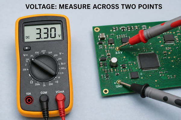
With power on, use DC voltage mode to check input voltage, regulator outputs, reference rails and connector pins. Always place the black probe on a known ground point and keep the red probe steady to avoid slipping across adjacent pins.

Multimeter probes checking PCB test points for continuity, resistance and power rails
Multimeter checks are useful for continuity, resistance, diode direction and DC rail verification.

How to Check for Shorts Before Powering the PCB

Before applying power, check the main power inputs and low-voltage rails for abnormal shorts to ground. This is one of the safest ways to prevent damage during first power-up.

Measure resistance from each rail to ground and compare it with the expected circuit behavior. A microcontroller core rail, high-current processor rail or LED driver output may naturally show low resistance, so do not assume every low value is a fault. The better method is to compare with a known-good board, schematic expectation or design engineer feedback.

If a rail reads nearly zero ohms, inspect nearby capacitors, IC pins, solder joints, vias and connectors. For repair work, current-limited power injection and thermal observation can help locate the hot component, but this should be done carefully to avoid damaging the PCB.

How to Test PCB Continuity and Broken Traces

Continuity testing confirms whether two points are electrically connected. It is useful for checking traces, vias, connectors, fuses, jumpers and repair wires.

Place one probe at the starting point and the other at the expected connected point. A beep or low resistance usually means the connection exists. No beep can indicate a broken trace, damaged via, cold solder joint, cracked connector pin or wrong test point.

For dense boards, do not drag probes across fine-pitch pins. Use sharp probe tips, stable magnification and the schematic or netlist when available. On multilayer boards, a broken internal trace is harder to confirm without design files, X-ray inspection or specialist failure analysis.

How to Test Components on a PCB Board

Some components can be checked in circuit, but many readings are affected by parallel paths. Treat in-circuit component testing as a screening step, not always a final diagnosis.

Resistors can often be measured if the surrounding circuit does not create a lower parallel path. Diodes and LEDs can be checked with diode mode, but driver ICs and protection circuits may affect the reading. Capacitors may show charging behavior on a resistance range, but accurate capacitance or ESR testing usually needs a suitable meter and sometimes removal from the circuit.

ICs are harder to test directly with a multimeter. For IC-related faults, check supply pins, reset pins, clock behavior, enable pins, communication lines and output signals. An oscilloscope or logic analyzer is usually needed when the failure is dynamic.

Power-Up Testing: What to Watch

Power-up testing should use controlled voltage and current limits whenever possible. A bench power supply with current limiting can prevent a short from destroying traces, regulators or ICs.

Start with the correct input voltage and a conservative current limit. Watch current draw, smell, heat, LED behavior and voltage stability. If the current immediately hits the limit, disconnect power and return to short-circuit checks. If the current looks normal, verify each regulated rail and then check the board under its expected load.

For production boards, a test fixture is better than manual probing. A fixture can contact defined test pads, reduce operator error and record pass/fail results more consistently.

Functional Testing for PCB Boards

Functional testing checks whether the PCB performs its intended job, not only whether traces and voltages exist. This is the step that connects electrical checks with real product behavior.

Typical functional tests include firmware loading, communication checks, sensor input response, relay output, LED output, motor drive, RF response, display behavior or load testing. The correct test depends on the product. A power supply PCB needs load and ripple checks; a control board needs input-output logic checks; a communication board needs interface and signal checks.

For PCB assembly production, functional testing should be documented with fixtures, test limits, firmware version, sample records and failure codes. Without records, repeated failures become harder to trace back to design, assembly or component problems.

Common PCB Board Faults Found During Testing

PCB testing often finds a small set of recurring problems. Knowing these failure patterns helps engineers choose the right next test instead of guessing.

Fault Possible cause Useful check
No power output Input fault, fuse, regulator failure, reversed polarity Input voltage, fuse continuity, regulator pins
Board draws too much current Shorted capacitor, solder bridge, damaged IC Rail-to-ground resistance, current-limited power-up
Intermittent operation Cracked solder joint, connector issue, thermal stress Magnified inspection, gentle flex test, thermal observation
Communication failure Wrong pull-up, bad clock, solder fault, firmware issue Voltage levels, oscilloscope, logic analyzer
One component overheats Short, wrong part, overload, incorrect orientation Orientation check, current check, schematic review

PCB Testing Checklist Before Production

For production or supplier acceptance, PCB board testing should be repeatable. A clear checklist helps avoid depending on one engineer’s memory.

  • Confirm PCB revision, BOM revision and assembly drawing match the order.
  • Inspect solder joints, polarity marks, connector orientation and visible damage.
  • Check main input rail resistance before power-up.
  • Check continuity for critical nets, connectors, fuses and test pads.
  • Power the board with current limiting during first validation.
  • Measure all required voltage rails under normal load.
  • Verify clocks, reset lines, enable signals and communication interfaces when relevant.
  • Run firmware, fixture or product-level functional tests.
  • Record failure symptoms, measured values and repair actions.
  • Feed repeated failures back into DFM, DFT, assembly and supplier review.

When Do You Need Professional PCB Testing?

Professional testing is useful when manual checks cannot explain the failure, when the board is high value, or when the issue may affect production quality.

Manual multimeter checks are enough for many simple continuity and power faults. But dense multilayer PCBs, BGA assemblies, impedance-sensitive boards, high-current boards and intermittent failures often need AOI, X-ray, ICT, flying probe testing, boundary scan, functional fixtures or failure analysis support.

If the same defect appears across many boards, do not treat it as a one-off repair issue. It may come from stencil design, reflow profile, component substitution, layout weakness, fixture error, contamination or handling damage.

FAQ

How do you test a PCB board quickly?

Start with visual inspection, then use a multimeter to check shorts, continuity and main power rails. If the board passes those checks, power it with current limiting and run the intended functional test.

Can you test a PCB board with only a multimeter?

You can find many basic faults with a multimeter, including open traces, shorts, wrong resistance and missing DC voltages. Dynamic signal, firmware, timing and communication problems usually need an oscilloscope, logic analyzer or functional test fixture.

What multimeter mode is used for PCB testing?

Use continuity mode for connected paths, resistance mode for rail-to-ground checks, diode mode for diode junctions and DC voltage mode for powered rail checks. Choose the mode based on the fault you are trying to confirm.

How do you know if a PCB is bad?

A PCB may be bad if it has visible damage, abnormal rail resistance, missing voltage, excessive current draw, failed continuity, overheating parts or failed functional output. One symptom is rarely enough; confirm with a structured test sequence.

Should you power a PCB before checking for shorts?

No. Check critical power rails for shorts before applying power, especially on repaired boards, new prototypes and boards with visible solder issues. This reduces the risk of burning traces or damaging ICs.

What is the difference between PCB inspection and PCB testing?

Inspection looks for visible defects such as solder bridges, cracks and wrong orientation. Testing measures electrical behavior, continuity, voltage, current and function. A reliable quality process usually needs both.

Can a PCB pass visual inspection but still fail testing?

Yes. A board can look clean but still have hidden open vias, wrong component values, internal layer problems, firmware issues or signal faults. Visual inspection is only the first layer of quality control.

What tools are commonly used to test PCB boards?

Common tools include a microscope, digital multimeter, bench power supply, oscilloscope, logic analyzer, test fixture, AOI system, flying probe tester, ICT fixture and functional test station.

Final Thoughts

Testing a PCB board is safest when the process moves from visual checks to unpowered electrical checks, then controlled power-up and finally functional verification. This order helps catch obvious faults early while protecting the board from avoidable damage.

If you need PCB fabrication, PCB assembly, prototype validation or production support, BestPCBs can help review manufacturing requirements, testing needs and assembly risk before your board moves into mass production. Contact the engineering team at sales@bestpcbs.com for technical support and a quote.

You may also like

What are the 7 Types of PCB Testing Methods?
Thursday, March 19th, 2026

PCB testing methods are non-negotiable for building durable, high-performance printed circuit boards that perform consistently in every application. Whether you run a small-scale electronics workshop or a large industrial manufacturing facility, testing protects your final products from early failure and costly rework. Every electronic device, from household gadgets to industrial machinery, relies on PCBs to function correctly. Skipping thorough testing leads to avoidable setbacks, but targeted testing processes streamline production and build customer trust. This guide breaks down every critical part of PCB testing, from basic definitions to step-by-step multimeter checks and industry compliance rules. You’ll learn practical techniques to elevate quality and keep your production line running smoothly.

PCB Testing Methods, https://www.bestpcbs.com/blog/2026/03/pcb-testing-methods/

What is PCB Testing?

PCB testing refers to structured checks run on printed circuit boards at several key production stages. It makes sure every board meets set design rules, electrical performance needs, and physical durability standards. These checks happen both before and after parts are assembled, covering blank circuit boards, half-finished units, and fully completed products.

Its main purpose is to find defects early, before boards go to full assembly or reach end users. Common small flaws include short circuits, open circuits, poor solder joints, broken wiring traces, and misplaced parts. With consistent targeted testing, these tiny issues never turn into costly failures later on. Good PCB testing also proves boards can handle daily use, normal temperature shifts, and regular wear without breaking down.

On top of catching defects, PCB testing confirms full board function and long-term durability. It ensures each board matches the original design files and works as intended in its final device. This testing works for rigid boards, flexible boards, and rigid-flex hybrid boards alike. No matter the PCB type, consistent testing helps you make reliable products that stand out in competitive markets.

What are the 7 Types of PCB Testing Methods?

Each method targets specific flaws and fits different production stages, creating a full coverage safety net for your boards.

First up is Visual Inspection, the most accessible initial testing step. Trained technicians examine bare boards and assembled units for visible defects like cracked traces, cold solder joints, misplaced components, or damaged substrate material. Many teams pair manual checks with automated optical inspection (AOI) for faster, more precise results. This method catches surface-level issues quickly and keeps early-stage defects from moving forward.

Second is Automated Optical Inspection (AOI), a tech-driven upgrade to manual visual checks. AOI machines use high-resolution cameras to scan PCBs and compare them to digital design files. It spots tiny defects human eyes might miss, such as insufficient solder or shifted micro-components. This method works well for mass production and cuts down on human error significantly.

Third is In-Circuit Testing (ICT), which checks individual components and electrical connections on assembled boards. ICT uses a bed of nails fixture to contact specific test points on the PCB. It verifies component values, checks for short or open circuits, and confirms proper part placement. This method delivers fast, accurate results for high-volume production runs.

Fourth is Flying Probe Testing, ideal for low-volume production or prototype boards. Unlike ICT, it uses movable probes instead of fixed fixtures, so no custom tooling is needed. Flying probes test individual points one by one, checking for opens, shorts, and component functionality. It’s cost-effective for small batches and quick prototype validation.

Fifth is X-Ray Inspection, designed for hidden defects that visual checks can’t find. It peer beneath solder joints, ball grid arrays (BGAs), and embedded components. X-ray testing detects cold joints, voids in solder, and internal wiring flaws common in dense, multilayer PCBs. This method is critical for high-complexity boards used in medical and aerospace gear.

Sixth is Functional Circuit Testing, which evaluates the PCB’s full operational performance. Testers power the board and run it through real-world operating conditions to confirm it does its intended job. This test checks overall functionality, not just individual parts, ensuring the board works as a complete unit.

Seventh is Environmental Testing, which checks durability under harsh conditions. Boards undergo temperature cycling, humidity exposure, vibration testing, and shock resistance checks. This ensures PCBs hold up in extreme environments, from industrial factories to outdoor electronic devices.

What are the 7 Types of PCB Testing Methods, https://www.bestpcbs.com/blog/2026/03/pcb-testing-methods/

What are the Most Common PCB Functional Testing Methods?

Building on the customer-focused benefits above, here are the most practical functional PCB testing methods, sorted by production scale, with clear value for your orders and projects.

  • Manual Functional Testing: Suited for low-volume orders, custom prototypes and small-batch specialized PCBs. Technicians connect the board to power and test tools, run performance checks manually, and monitor voltage, signals and response speed to confirm full function.
  • Automated Functional Testing (AFT): Designed for high-volume mass production. Pre-programmed systems run full performance tests without constant manual oversight, auto-power the board, log test results and finish checks quickly.
  • Boundary Scan Testing: Made for dense, high-tech PCBs with limited test points (like BGA and compact surface-mount boards). Uses built-in component circuitry to test connections without direct probe contact.
  • Built-In Self-Test (BIST): Integrates auto-diagnostic functions directly into the PCB or its components. The board runs self-checks when powered on, no external test equipment needed.

What are the Benefits of Using PCB Functional Testing Methods?

After covering core PCB testing types, let’s break down the customer-focused benefits of functional PCB testing, with clear, actionable advantages that directly protect your interests and boost your business gains.

  • Cut down product failures and after-sales troubles: Functional testing weeds out faulty boards before delivery, so your end customers get fully working PCBs that don’t break down early. This slashes product returns, warranty claims and costly after-sales repairs, and keeps your customers satisfied and loyal for repeat orders.
  • Lower your total production costs: It catches defects before finished boards are packaged and shipped, avoiding the high cost of reworking fully assembled units. Less material waste and fewer rework hours add up to big long-term cost savings for your project and business.
  • Ensure stable, consistent product quality: Every board you receive meets the same strict performance standards, with zero quality fluctuations between batches. This builds a reliable reputation for your products, and helps you win trust from clients in high-demand, critical industries.
  • Speed up order delivery and market launch: Boards pass final checks smoothly and move to shipping quickly, with no delays from last-minute defect fixes. It also eases industry regulatory compliance, as valid functional test results help you get market approval faster.
  • Support better product design and fewer recurring flaws: Test data gives clear insights to optimize PCB design and production processes, fixing repeated quality issues. You get more stable, durable boards for future orders, with less risk of consistent defects.
What Are the Benefits of Using PCB Functional Testing Methods, https://www.bestpcbs.com/blog/2026/03/pcb-testing-methods/

What is the Standard PCB Testing Procedure for Quality Control?

With individual testing methods covered, let’s outline a standard, repeatable PCB testing procedure for consistent quality control. Following this step-by-step workflow ensures no defects slip through the cracks at any production stage.

Step 1: Pre-production design review and test point planning. Before manufacturing starts, engineers mark clear test points on the PCB design for easy access later. This ensures every critical area can be tested efficiently once production begins.

Step 2: Bare board testing on raw substrates. Test for open circuits, short circuits, and trace integrity before any components are added. Fixing flaws at this stage is far cheaper than after assembly.

Step 3: Post-solder inspection right after component assembly. Use AOI or visual checks to spot immediate solder defects before moving to electrical testing. This catches quick fixes early and prevents further processing of faulty units.

Step 4: In-circuit or flying probe testing to check individual components and electrical connections. Verify each part functions correctly and connects to the board as intended.

Step 5: Full functional testing to simulate real-world operation. Power the board and run it through all intended functions to confirm complete performance compliance.

Step 6: Environmental and durability testing for high-reliability applications. Subject boards to stress tests to ensure they hold up in harsh conditions.

Step 7: Final quality check and documentation review. Log all test results for compliance and record-keeping, then approve passing boards for shipping.

This standardized procedure creates a transparent, repeatable system that scales from small prototypes to large production batches. It keeps quality consistent and provides clear documentation for client and regulatory needs.

How to Test PCB Board with Multimeter?

For quick, on-the-spot testing without advanced equipment, a multimeter is a reliable and affordable tool. Follow this simple step-by-step guide to test PCBs safely and effectively with a standard multimeter.

First, prepare your workspace and multimeter. Turn off and disconnect the PCB from all power sources to avoid injury or equipment damage. Set your multimeter to the continuity test mode, marked with a sound wave or diode symbol.

1. Test for short circuits. Touch one multimeter probe to a power trace and the other to a ground trace. A continuous beep means a short circuit is present; no beep means the path is clear.

2. Check for open circuits. Touch both probes to the two ends of a single PCB trace or component lead. A solid beep confirms a closed, working circuit; no beep means an open circuit that needs repair.

3. Test diode and component polarity. Switch the multimeter to diode mode and touch probes to diode leads. Properly functioning diodes show a specific voltage reading in one direction only, confirming correct polarity.

4. Check resistance values for resistors. Set the multimeter to the correct resistance range and touch probes to resistor leads. Compare the reading to the resistor’s labeled value to confirm it functions properly.

5. Verify voltage regulation (for powered boards, only if safe). Once the board is powered correctly, set the multimeter to voltage mode and check voltage at designated test points. Confirm readings match the design specifications for stable performance.

6. Document your findings and mark faulty boards. Log any abnormal readings for repair, and set aside non-functional boards for rework. Always double-check suspicious readings to rule out user error.

This multimeter method is perfect for quick prototype checks, small-batch testing, and field repairs. It’s a handy skill for technicians and engineers working with PCBs in any setting.

How to Test PCB Board with Multimeter, https://www.bestpcbs.com/blog/2026/03/pcb-testing-methods/

What PCB Testing Standards Should Manufacturers Follow?

Following global PCB testing standards ensures consistent quality, cross-market compliance, and predictable performance for every order. These standards set clear, objective rules for testing, defect thresholds, and final product acceptability.

  • IPC-A-600: Core standard for bare printed circuit boards; defines clear acceptability criteria for visual and electrical checks. It separates qualified boards from defective ones at the raw substrate stage, preventing flawed blank boards from moving to assembly.
  • IPC-J-STD-004: Focused on solder joint quality and assembled PCB testing; sets strict rules for solder joint inspection, rework limits, and final acceptance. It eliminates weak or unreliable solder connections, the top cause of PCB field failures.
  • IPC-925: Covers reliability-focused testing and quality compliance protocols; includes environmental testing, durability verification, and long-term performance validation. It ensures boards hold up under real-world stress and extended use.
  • ISO 9001: Global quality management standard for full production and testing workflows; ensures consistent, repeatable testing processes across all batches. Compliance proves a commitment to stable quality and continuous process improvement for international markets.
  • IPC-6012 (for critical applications): Strict standard for rigid PCBs used in medical, aerospace, and high-reliability industrial devices. It meets tight industry safety and performance rules for products where failure is not an option.

How Do PCB Testing Methods Ensure Quality Control in Production?

Here are PCB testing methods ensure quality control in production:

  • Automated Optical Inspection (AOI): Uses high-speed cameras and AI algorithms to detect solder defects, missing components, and alignment errors on PCBs. Ensures visual quality control by identifying surface-level flaws early in production.
  • X-ray Inspection: Penetrates PCB layers to inspect hidden solder joints (e.g., BGAs, QFNs) for voids, cracks, or misalignments. Critical for verifying internal quality without physical disassembly.
  • Flying Probe Testing (FPT): Employs movable probes to test electrical connections, continuity, and isolation between PCB nodes. Validates circuit functionality and detects open/short circuits with high precision.
  • In-Circuit Testing (ICT): Uses fixed test probes to verify component values, polarity, and circuit performance. Ensures all electrical parameters meet design specifications before functional testing.
  • Functional Testing: Simulates real-world operating conditions to validate PCB performance under load. Confirms end-to-end functionality, power stability, and signal integrity.
  • Boundary Scan (JTAG): Tests digital circuits via IEEE 1149.1 standard to verify connectivity and detect faults in embedded devices. Ideal for complex boards with limited physical access points.
  • Thermal Imaging: Monitors heat distribution across PCBs to identify hotspots or cooling issues. Prevents thermal-related failures by ensuring components operate within safe temperature ranges.
  • Acoustic Microscopy: Uses high-frequency sound waves to detect delamination, cracks, or voids in PCB substrates. Ensures material integrity and structural reliability.

Whether you’re new to PCB manufacturing or looking to upgrade your existing quality control process, choosing the right PCB testing methods and following consistent procedures makes all the difference. By combining manual checks, automated equipment, and digital software, you can build a robust testing system that delivers reliable, high-performance PCBs every time.

You may also like

What is ICT Tester? In Circuit Test vs Flying Probe Testing
Monday, August 18th, 2025

Have you ever wondered why some electronic devices fail even when the PCB looks flawless? Or why high-volume production sometimes delivers inconsistent boards? These issues often trace back to undetected component defects, poor soldering, or faulty connections. Without proper testing, even a single defective part can lead to product failure, costly recalls, or customer dissatisfaction.

This is where an ICT tester equipment comes in. By performing in-circuit testing (ICT), manufacturers can quickly detect missing components, shorts, opens, and incorrect placements before the boards leave the production line. With the right ICT test electronics and in-circuit test fixtures, you gain fast, accurate, and reliable validation of each PCB, saving both time and money.

In this article, we’ll answer key questions such as:

  • What exactly is an ICT tester, and how does it work?
  • Why is ICT testing so critical for electronics manufacturing?
  • How does ICT differ from functional testing or flying probe testing?
  • When should you use ICT versus functional testing for your boards?

By understanding these points, you’ll see how ICT testing can prevent defects, improve production efficiency, and ensure reliable end products—turning potential headaches into controlled, predictable outcomes.

What is an ICT Tester?

An ICT tester is a system designed to perform in-circuit testing (ICT) on printed circuit boards after assembly. It is often recognized by its “bed-of-nails” fixture, which has hundreds or even thousands of pins arranged to contact specific points on the PCB. Each pin corresponds to a pad, via, or test point, allowing the tester to measure voltages, resistances, and currents at component level.

ICT testers can:

  • Detect missing, incorrect, or faulty components.
  • Identify open circuits, short circuits, and soldering defects.
  • Measure parameters such as resistance, capacitance, and diode orientation.
  • Verify integrated circuit placement and connectivity.

Because ICT is thorough and fast, it has become an industry-standard approach, especially in high-volume production lines.

Why is the ICT Test Important?

The ICT test is important for several reasons. In large-scale manufacturing, even a single defect can ripple into thousands of defective units. Detecting issues early reduces costs, avoids recalls, and protects brand reputation.

For example, in automotive electronics, where safety systems depend on flawless PCBs, ICT is crucial. An undetected fault in an airbag control system could have serious consequences. In consumer electronics, ICT prevents faulty smartphones, laptops, or home appliances from reaching the market.

The ICT test is also important for process improvement. It provides engineers with statistical data that highlights recurring problems, such as solder bridging or component misplacement. Manufacturers can use this data to refine processes, reduce defect rates, and improve yields.

What is the Purpose of the ICT Test?

The main purpose of ICT testing is to validate the quality and functionality of each component on the PCB. Unlike functional testing, which looks at the board’s overall behavior, ICT digs into details at component level.

ICT ensures that:

  • Every resistor has the correct value.
  • Capacitors and inductors are present and within tolerance.
  • Diodes and transistors are oriented properly.
  • Integrated circuits are placed in the right sockets and connected.

By catching defects at the source, ICT reduces the risk of failures at the product’s final stage. This is especially valuable in industries where long-term reliability is critical, such as aerospace, defense, and medical devices.

How Does an ICT Tester Work?

An ICT tester works by pressing the in-circuit test fixture against the PCB, making contact with the test pads or vias. Once contact is established, the system injects signals into the board and records the response.

Here’s a breakdown of the process:

  • Fixture Setup – The board is placed into a bed-of-nails fixture designed for its exact layout.
  • Signal Injection – Test probes inject electrical signals into various nodes of the circuit.
  • Measurement – The tester measures voltage, current, resistance, and capacitance at each point.
  • Analysis – Software compares the measured values with predefined thresholds.
  • Reporting – The system highlights any failures or deviations for quick troubleshooting.

ICT is highly automated, with a cycle time ranging from a few seconds to less than a minute. This makes it efficient for high-volume production, where time savings directly translate to lower manufacturing costs.

Advantages of ICT Testing

  • High Accuracy – Detects even subtle component defects.
  • Fast Cycle Time – Ideal for mass production.
  • Detailed Data – Provides insight into manufacturing trends.
  • Early Detection – Reduces rework and repair costs.
  • Reliability – Improves long-term performance of products.

What is the Difference Between Functional Testing and ICT Testing?

Both functional testing and ICT testing play important roles in quality assurance, but they target different aspects of the PCB.

  • ICT Testing – Focuses on component-level verification. It checks each resistor, capacitor, diode, transistor, and IC independently. ICT identifies defects like shorts, opens, wrong components, or poor solder joints.
  • Functional Testing – Evaluates the overall system behavior. It simulates real-world operating conditions, ensuring the PCB performs its intended function. Functional testing may involve powering up the device, running software, or checking communication protocols.

To put it simply: ICT looks at how the board is built, while functional testing checks how the board behaves. Both tests are complementary, and many manufacturers use them together.

Functional Testing vs ICT Testing

When to Use ICT and Functional Testing?

Choosing between ICT and functional testing depends on project goals and production stage.

Use ICT testing when:

  • Boards are still in the manufacturing phase.
  • Component-level accuracy needs to be validated.
  • High-volume production demands fast, repeatable results.

Use functional testing when:

  • The assembly is nearly complete.
  • The product’s performance under real operating conditions needs to be verified.
  • System-level testing is required, such as communication between multiple boards.

For best results, many manufacturers use a combination of ICT and functional testing. ICT catches early-stage defects, while functional testing provides final validation before shipment.

In-Circuit Test vs Flying Probe: What are Differences?

When comparing in-circuit testing (ICT) with flying probe testing, the differences come down to cost, speed, and flexibility.

In-Circuit Test (ICT):

  • Uses a custom in-circuit test fixture.
  • Offers fast cycle times (seconds).
  • Best for high-volume production.
  • High upfront cost for the fixture, but lower cost per test afterward.

Flying Probe Test:

  • Uses moving probes instead of a fixture.
  • Slower than ICT, since probes move sequentially.
  • Excellent for prototypes and low-volume runs.
  • No fixture cost, making it more flexible and cost-effective for small batches.

In practice, many manufacturers start with flying probe testing during prototyping. Once the design is finalized and volumes increase, they shift to ICT testing for efficiency.

In-Circuit Test vs Flying Probe

Applications of ICT Testing

ICT testing is used in a wide range of industries:

  • Automotive – For safety-critical systems like airbags, ABS, and engine control units.
  • Medical Devices – For life-support systems, imaging equipment, and diagnostic tools.
  • Aerospace and Defense – Where reliability under extreme conditions is non-negotiable.
  • Consumer Electronics – From smartphones to laptops, ensuring consistent quality.
  • Industrial Equipment – For automation controllers and power management systems.

In each of these cases, ICT contributes to higher reliability, lower failure rates, and better compliance with international standards.

Why Choose EBest Circuit (Best Technology) for ICT and PCB Testing?

EBest Circuit (Best Technology) is a reliable PCB manufacturer in China, trusted by more than 1,000 customers across industries worldwide. We specialize in small to medium-volume PCB manufacturing, PCB assembly, and complete electronic manufacturing services.

As one of the most experienced circuit board suppliers, our capabilities cover a wide range of PCB types, including rigid PCBs, flex PCBs, rigid-flex PCBs, aluminum PCBs, RF/microwave PCBs, high-speed and high-frequency PCBs, and HDI PCBs. Beyond manufacturing, we also provide turnkey assembly, component sourcing, box build assembly, PCBA testing, and full electronic testing services.

With over 19 years of experience, our engineering, production, and quality teams fully understand the unique needs of industries such as medical, automotive, and aerospace. We strictly follow international standards, working under IPC-A-600 for PCB manufacturing and IPC-A-610 for PCB assembly. All of our products meet IPC Class 2 standards, and for projects requiring higher reliability, we also deliver Class 3 or Class 3A compliance. Combined with strong engineering support and competitive pricing, we help customers achieve both reliability and cost-effectiveness.

FAQs

1. What does ICT stand for in electronics testing?

ICT stands for in-circuit testing, which validates the quality of individual PCB components.

2. Can ICT testing replace functional testing?

No. ICT and functional testing serve different purposes. ICT checks construction, while functional testing checks performance.

3. How long does an ICT test take?

Most ICT tests take only a few seconds, depending on the number of test points.

4. Is an in-circuit test fixture reusable?

Yes, but each fixture is custom-designed for a specific PCB layout.

5. Which is better: in-circuit test or flying probe?

ICT is best for high-volume runs due to speed. Flying probe is better for prototypes or small batches.

You may also like

Printed Circuit Boards: PCB Design, Fabrication, Assembly and Testing
Friday, June 6th, 2025

When creating modern electronic devices, every step matters – from the first sketch to the final product. If you’re exploring the process of printed circuit boards, or PCBs, this guide is your one-stop resource. We’ll walk through PCB design, fabrication, assembly, and testing, covering what engineers and buyers need to know. Whether you’re designing your first board or sourcing from a manufacturer, getting each step right ensures performance, reliability, and cost-efficiency.

Printed Circuit Boards: PCB Design, Fabrication, Assembly and Testing

What Is a Printed Circuit Board?

A printed circuit board (PCB) is the backbone of nearly all electronic systems. It’s a flat board that holds and connects electronic components using conductive tracks, pads, and vias etched from copper sheets laminated onto a non-conductive substrate. Common materials include FR4, ceramic, aluminum, and polyimide.

PCBs come in many forms: single-sided, double-sided, and multilayer PCB, supporting everything from simple gadgets to complex military electronics. Their role is simple yet critical: provide physical support and reliable electrical connections.

How to Design a PCB Board?

The PCB design phase sets the tone for the entire lifecycle. It begins with defining the schematic, which maps out the electronic connections between components. Once that’s ready, designers move to layout – placing components and routing traces.

Key steps include:

  1. Creating schematics using software like Altium Designer, KiCAD, or Eagle.
  2. Assigning footprints to components for proper placement.
  3. Defining board dimensions, layer stack-up, and signal flow.
  4. Routing signals with attention to trace width, impedance, and clearance.
  5. Adding vias, copper pours, and power planes for optimal performance.
  6. Design Rule Check (DRC) to verify spacing, trace width, and other constraints.
  7. Generating Gerber files, which are the manufacturing blueprints.
Printed Circuit Boards: PCB Design, Fabrication, Assembly and Testing

Each design must balance space, power, heat, cost, and manufacturability. One overlooked detail could delay your entire project.

Considerations During PCB Design Phase

Designers must juggle multiple variables beyond schematic accuracy. Here are essential considerations to optimize performance and reduce failure risks:

1. Component Placement: Keep analog, digital, and power circuits separate to reduce interference. Group related components logically to minimize trace lengths.

2. Signal Integrity: For high-speed designs, impedance matching, differential pair routing, and minimizing crosstalk are vital.

3. Thermal Management: Use thermal vias, copper pours, and heat sinks to handle heat dissipation—especially in power electronics.

4. Design for Manufacturability (DFM): Ensure trace width, drill sizes, and clearances match manufacturer capabilities.

5. EMC and EMI Compliance: Ground planes, shielding, and filtering components help meet regulatory standards.

6. Mechanical Constraints: Don’t overlook mounting holes, connector alignment, or enclosure fit. These small details can turn into costly errors later.

Good design minimizes rework, improves lifespan, and lowers costs across production.

Full PCB Fabrication Process – Step by Step

Once the design is complete, the PCB fabrication process turns digital files into a tangible board. Here’s how it happens:

1. Material Selection

The manufacturer selects base materials like FR4, aluminum, or ceramic depending on thermal, mechanical, and electrical requirements.

2. Inner Layer Imaging (for Multilayer PCBs)

Each inner copper layer is patterned with the circuit using photoresist, UV exposure, and etching techniques.

3. Lamination

The etched inner layers are stacked and laminated under heat and pressure, forming a solid multilayer structure.

4. Drilling

Holes are drilled to create vias for electrical connections between layers. Laser drilling is used for microvias.

5. Plating and Copper Deposition

Holes are plated with copper using electroplating to ensure conductivity across layers.

6. Outer Layer Imaging

Outer copper layers are patterned similar to the inner layers using photoresist and etching.

7. Solder Mask Application

A solder mask is applied to insulate the board and protect traces, leaving pads and holes exposed for soldering.

8. Silkscreen Printing

Component labels, logos, and reference indicators are printed on the board.

9. Surface Finish

A surface finish like HASL, ENIG, OSP, or Immersion Silver is applied to exposed copper pads to protect them and improve solderability.

10. Electrical Testing

Flying probe or bed-of-nails tests check for open circuits and shorts.

Common PCB Assembly Issues During Manufacturing

During PCB assembly, components are mounted and soldered onto the board. This phase can be manual or automated using SMT (surface-mount technology) and THT (through-hole technology).

But several issues can disrupt this process:

1. Tombstoning: A component lifts on one side during reflow, causing connectivity failure.

2. Solder Bridges: Excess solder connects two pins unintentionally, leading to short circuits.

3. Cold Joints: Poor soldering results in weak mechanical bonds and unreliable connections.

4. Misaligned Components: Incorrect placement, often caused by poor paste application or pick-and-place calibration.

5. PCB Warping: Thin or large boards may bend during reflow, affecting soldering and mechanical integrity.

6. Component Damage: Excessive heat or mishandling can destroy delicate ICs or capacitors.

Quality control, professional assembly lines, and well-prepared Gerber + BOM files help avoid these issues.

How to Test Printed Circuit Boards?

After assembly, PCB testing ensures the product works before final integration. There are several testing levels depending on the application and budget:

Printed Circuit Boards: PCB Design, Fabrication, Assembly and Testing

1. Visual Inspection

The simplest method. Engineers check for physical defects like solder bridges, missing components, or alignment issues.

2. Automated Optical Inspection (AOI)

AOI uses cameras to scan boards for soldering quality, polarity, and presence of components.

3. In-Circuit Testing (ICT)

Tests each component’s electrical characteristics by probing specific test points. It’s fast and accurate for large-volume production.

4. Flying Probe Testing

Uses robotic probes to test low-to-medium volume PCBs without the need for custom fixtures.

5. Functional Testing (FCT)

Verifies the complete assembled PCB in real-world operating conditions. Essential for high-reliability applications.

Testing isn’t optional—it’s critical. Faulty boards cost time, money, and customer trust.

Why Consider EBest Circuit (Best Technology)’s Turnkey Service?

If you’re tired of juggling multiple vendors for PCB design, fabrication, assembly, and testing, EBest Circuit (Best Technology) offers a full turnkey PCB service that simplifies the process.

Here’s why clients worldwide trust us:

◎ Technical Support Before & After Sales

◎ Prototype & Small Volume Welcome

◎ Quick Turn-out, On-time Delivery

◎ High Quality, Special Request Available

◎ Strong R&D Team, Know How-To

◎ Rich Experience (>13 Years)

◎ Prompt Feedback (within 12H)

◎ One-stop Service (PCBA/Assembly)

Conclusion

Printed circuit boards are at the heart of modern electronics, and getting the design, fabrication, assembly, and testing right is non-negotiable. Each step has its role—and skipping or rushing any part can lead to costly failures.

Whether you’re building a simple sensor or a complex industrial controller, choosing a partner like EBest Circuit (Best Technology) can make the journey smoother. We understand what engineers, startups, and procurement teams need: fast delivery, quality control, and transparent communication.

FAQs

1. What software is used to design PCBs?

Tools like Altium Designer, Eagle, KiCAD, and OrCAD are commonly used for schematic and PCB layout.

2. How long does PCB fabrication take?

Standard fabrication takes 3–7 days. Express services can deliver in 24–48 hours depending on complexity.

3. What is the difference between PCB and PCBA?

PCB is the bare board. PCBA is the board after components are assembled and soldered.

4. How much does PCB assembly cost?

Costs vary based on quantity, complexity, part types, and whether parts are sourced by the manufacturer or supplied by the customer.

5. Does EBest Circuit (Best Technology) support low-volume PCB manufacturing?

Yes. We support both low and high-volume production and offer prototyping services for new designs.

You may also like

What is ate in pcba testing?
Thursday, September 26th, 2024

Automatic test equipment (ATE) plays a vital role in the field of electronic manufacturing, especially in the testing of printed circuit board assemblies (PCBA). In order to ensure the quality of PCBA, automatic test equipment (ATE) has become an indispensable force in the PCBA testing process with its high efficiency, accuracy and reliability.

What are the 7 types of PCB testing methods?

The common detection methods of PCB (Printed Circuit Board) boards are mainly used to detect the quality and accuracy of PCB boards, which is an indispensable part of the PCB production process. The following are 7 commonly used PCB board detection methods:

  • 1. Visual inspection: Visual inspection is the simplest detection method. It observes the surface of the PCB board with human eyes to find possible defects, such as welding problems, component position offset, etc.
What is ate in pcba testing?
  • 2. X-ray detection: X-ray detection is mainly used to detect problems hidden inside the PCB board, such as welding quality, BGA ball welding quality, inner layer line routing problems, etc.
  • 3. Non-destructive testing: Non-destructive testing is a non-destructive detection method. Commonly used technologies include infrared testing, ultrasonic testing and electromagnetic wave testing.
  • 4. AOl (Automated Optical Inspection): AOl is a method of automated inspection using optical equipment, which detects problems on the surface of PCB boards through high-resolution camera systems and pattern recognition software.
  • 5. ATE (Automatic Test Equipment): ATE is an automatic test equipment used to test the electrical performance and functions of PCB boards.
  • 6. Vibration test: Vibration test is used to detect the reliability and durability of PCB boards in vibration environments. By applying vibrations of different frequencies and amplitudes, the problems that may occur in actual use of PCB boards can be evaluated.
  • 7. Thermal shock test: Thermal shock test is used to detect the performance of PCB boards in temperature change environments. By rapidly changing the temperature, the thermal expansion, thermal stability and welding quality of PCB boards can be evaluated.

These methods can comprehensively evaluate the quality and performance of PCB boards and detect potential problems in a timely manner to ensure the reliability and stability of PCB boards.

What is ate testing in semiconductor?

ATE testing is an important link in the semiconductor industry for testing the functional integrity and reliability of integrated circuits (ICs). It is the abbreviation of Automatic Test Equipment, which is a device that tests devices, circuit boards, and subsystems through computer control.

ATE testing plays a vital role in the semiconductor manufacturing process. It is a key step to ensure the quality of IC products. The test content includes DC parameter testing, AC parameter testing, functional testing, etc. These tests are designed to evaluate the performance, function, and reliability of the chip.

The basic principle of the test is to apply stimulus to the chip through the test vector, measure the response output of the chip, and compare it with the expected result to determine whether the chip meets the specification requirements.

ATE testing not only involves testing various parameters of the chip, but also includes structural testing of the chip, that is, detecting manufacturing defects to ensure the quality and reliability of the chip.

In addition, ATE testing also includes testing of voltage, current, frequency, pulse, temperature and other aspects of the chip to achieve comprehensive testing of the static parameters and dynamic performance of semiconductor chips.

In general, ATE testing is an important means of quality control of integrated circuits in the semiconductor industry. It improves the efficiency and accuracy of testing through automation, ensures the quality and reliability of semiconductor chips, and is an indispensable and important link in the semiconductor manufacturing process.

What is an ATE PSU?

ATE PSU refers to the power supply unit (Power Supply Unit) of Automatic Test Equipment. In the field of electronic testing, ATE (automatic test equipment) is mainly used for integrated systems of power supply electrical performance testing. The system consists of test equipment hardware and test system software, and is designed to provide efficient and accurate automatic testing functions.

What is ate in pcba testing?

The key to ATE test system integration is to combine test software, test hardware (such as oscilloscopes, digital multimeters, vector networks, etc.) with communication technology to meet the testing needs of products. With the increasing complexity of electronic products, the role of ATE test system integration has become indispensable.

As part of the ATE system, the power supply unit (PSU) is responsible for providing a stable power supply for the entire test system to ensure the accuracy and reliability of the test.

Therefore, ATE PSU is one of the very important components in the ATE system, and its performance directly affects the overall efficiency and accuracy of the ATE test system.

What are the advantages of ATE?

ATE test system has the following significant advantages:

  • ‌High efficiency and time saving‌: ATE test system can automatically complete the test without manual intervention, which greatly saves test time and improves production efficiency‌.
  • ‌Easy to operate‌: The operation is simple and easy to understand, easy to get started, which reduces the skill requirements for operators and reduces training costs‌.
  • ‌Safe and reliable‌: The danger of manual operation can be avoided during the test process to ensure the life safety of employees‌.
  • ‌Improve test efficiency‌: Automatically execute the test program, greatly shorten the test cycle, reduce manual intervention, and thus significantly improve test efficiency‌.
  • ‌Flexibility and scalability‌: It can be flexibly configured and adjusted according to different test requirements, and supports customized configuration of various test modules and sensors‌.
  • ‌Reduced labor costs‌: Reduced dependence on labor, reduced labor costs, and improved labor efficiency‌.
  • ‌Strong anti-interference ability‌: The internal mechanical properties are good, and various external interferences can be eliminated to ensure the stability and accuracy of the test results‌.

In summary, the ATE test system is of great significance in improving production efficiency, reducing costs, ensuring employee safety, and optimizing quality management. It is widely used in product testing in semiconductors, electronics, automobiles and other fields‌.

What is ate in PCB?

ATE in PCB refers to automatic test equipment (Automatic Test Equipment). ATE is a computer-controlled device used to test devices, circuit boards, and subsystems.

It replaces manual labor through computer programming and automatically completes the test sequence. In the semiconductor industry, ATE specifically refers to an automatic tester for integrated circuits (ICs), whose functions include detecting the integrity of integrated circuit functions and ensuring the quality of integrated circuit manufacturing.

In a broader context, ATE equipment can perform chip parameter testing, functional testing, performance testing, fault detection, reliability testing, etc., and plays a vital role in the semiconductor manufacturing process.

What is the difference between automatic and manual testing?

In PCB testing, there are the following differences between automatic testing and manual testing:

  • 1. Automatic testing relies on equipment and software, and is programmed; manual testing is manually operated and more flexible.
  • 2. Automatic testing is high-speed and efficient, and can run continuously; manual testing is slow, easy to fatigue and low efficiency.
  • 3. Automatic testing has high accuracy and good consistency; manual testing is easily affected by human factors and has poor consistency.
  • 4. Automatic testing equipment has high investment but low operating cost; manual testing equipment has low cost but high labor cost.
  • 5. Automated testing is suitable for large-scale production and complex circuit boards; manual testing is suitable for small-batch production and fault diagnosis.

What is the purpose of automated testing?

The purpose of automated testing in PCB is to ensure that each circuit board can meet the high performance required in complex electrical applications, and to improve product quality and performance by detecting and repairing defects. ‌

Automated testing, especially in the PCB (printed circuit board) production process, plays a vital role. This test uses machine scanners with light imaging to visually inspect the finished circuit board and evaluate the process quality by using technologies such as automated optical inspection (AOI).

What is ate in pcba testing?

The importance of automated testing lies in its ability to detect and repair defects at multiple stages of production, including bare board inspection, solder paste inspection, pre-reflow and post-reflow. Improve production speed and productivity to ensure that tasks are completed on time.

Conclusion:

Automated test equipment (ATE) plays a key role in PCBA testing. It can improve test efficiency, accuracy and product quality, reduce test costs, and provide strong support for electronic manufacturing companies. With the continuous development of electronic technology, ATE will also continue to upgrade and improve to adapt to the increasingly complex PCBA testing needs.

You may also like

What is a E-Tester & how E-tester test PCB?
Saturday, December 2nd, 2023

We often receive this question from customer” what is a E-Tester?” and” how to do E-Test for FR4 PCB?” Hereby I would like to share with you how to use E-Tester to test PCB.

EBest Circuit (Best Technology) in FR4 PCB circuit manufacturing filed since year 2006, we have more than 17 years experiences in PCB fabrication process. We can provide from the design to turn key service for our customer.

Let us come to today’s topic, now what is a E-Tester?

What is a E-tester?

E-Tester is tooling for test PCB during volume production. E-Tester was used to detect the electrical performance of PCB. It is the essential process to test the PCB by this tester before shipment.

As you may know that during PCB process flow, it might be caused some defects by external factors and this is unavoidable.

So, in order to reduce the loss before PCB goes to the next stage when it is assembled with components, Therefore, the E-Test plays important role in PCB quality control to segregate PCBs with defects from shipment to customers and that’s why most of customers require their PCB manufactures to do 100% E test before shipment.

(E_testers)

The E tester mainly checks the open/short circuit for FR4 PCB.

How to do E-test?

Firstly, set up the E-tester on the testing machine and up test datasheet on the computer. Put the board to the E-tester to test the open/short circuit for board and dielectric strength.

Shorts Test: Check to make sure that NO current flows between separate nets by measuring the amount resistance between them.

Opens Test: Check to make sure there is current flow from one “node” to the next for every net on the board.

(Tester_testing)

During the testing, test whether there is short circuit between different network routes of PCB; test whether the PCB network is open to each PAD, and whether the hole is open; Finally, Insulation strength test and the Impedance test.

If the trace open is found on the bare board, the failure location could be repaired or the bare board has to be scrapped. On the other hand, the cost will be increased when PCB goes to the next stage when it is assembled with components, mainly are the sorting cost, component cost and the assembly cost. The compensation ratio is 10 times or even more than the PCB cost and this damages PCB manufacturer’s profit. The worse case is when PCBA is installed onto the end product, the loss caused by defected PCB could be very painful, say up to thousand times of PCB cost. Therefore, the E-Test plays important role in PCB industry to segregate PCBs with defects from shipment to customers and that’s why most of customers require their PCB suppliers to do 100% E test before shipment.

If you want to know more about testing for FR4 PCB board, welcome to visited www.bestpcbs.com or email us, we are very happy to answer your question.

You may also like