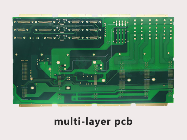
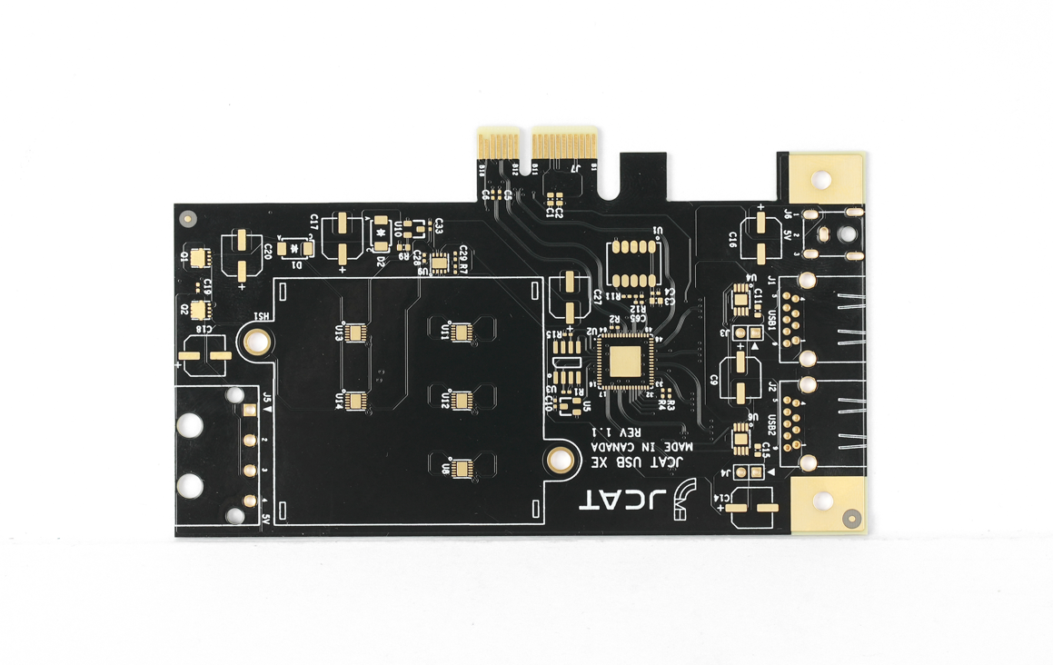
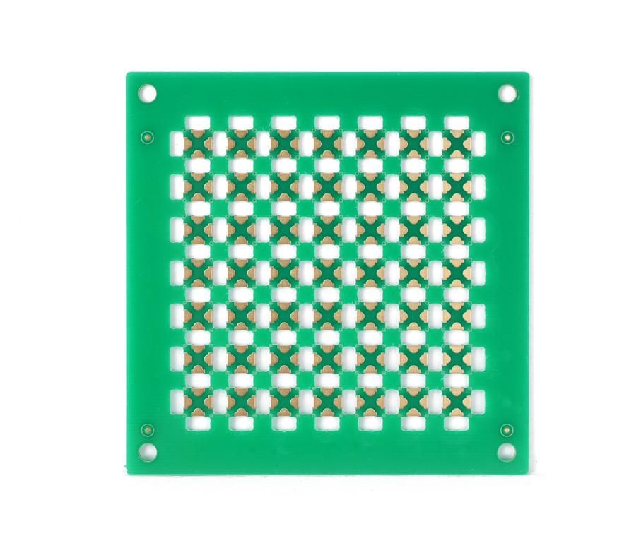
IPC-A-600 gives PCB manufacturers and customers a common visual reference for judging bare-board workmanship. It is used alongside the agreed performance specification, product class and drawing requirements. At EBest Circuit (Best Technology), we manufacture custom PCBs and provide inspection and testing capabilities that help evaluate the boards before assembly. For your project, the practical question is how these requirements and checks relate to solderable pads, sound interconnections and the circuit you expect to receive.
What Is IPC A 600, and Why Does It Matter for Your PCB?
The IPC A 600 standard is an illustrated acceptability reference for unassembled printed boards. Its title, IPC A 600 Acceptability of Printed Boards, covers the board itself: the conductive pattern, laminate and interconnections that will later support your components. It is not an assembly solder-joint standard.
For a customer, a shared reference makes a quality discussion more specific. A pad, hole or board edge can be evaluated against an agreed requirement instead of an impression that it looks unusual. For us as a fabricator, that same distinction connects the intended board construction with the features that need examination. Appearance is one part of acceptance; measurements and testing supply the additional evidence required by the design.
Which IPC-A-600 Revision Applies to Your Order?
The revision agreed for your order is the applicable baseline. The IPC A 600 latest revision is IPC-A-600M, released in May 2025. A repeat order may still reference an earlier edition; a newly released standard does not automatically change an existing contractual requirement.
Using the IPC A 600 current revision for a new design and maintaining an established revision for an existing product are different decisions. We can discuss the revision stated in your fabrication requirements as part of the engineering review. This helps keep the requested board, inspection expectations and subsequent repeat builds aligned.
An authorized IPC A 600 PDF or printed copy contains the detailed criteria for the selected edition. This article explains their role in PCB manufacturing; the complete standard and your agreed specification remain the references for individual acceptance decisions.
How Do Class 2 and Class 3 Affect PCB Acceptance?
The product class expresses the service expectations behind the acceptance requirements. In an IPC A 600 class 2 vs class 3 comparison, the useful distinction is the intended level of service, not the appearance of the finished board or a universal quality ranking.
Class reference
Service expectation
Meaning for your board
IPC A 600 class 2
Dedicated-service products requiring extended life and continued performance
The specified Class 2 criteria establish the relevant acceptance baseline.
IPC A 600 class 3
High-performance products where continued operation is especially important
The applicable Class 3 criteria and any additional requirements need to be reflected in the build requirements.
A drawing may use the wording IPC A 600 class II for Class 2. The class, revision and any customer-specific requirements together define what is requested. We can review those requirements against your stack-up and features before manufacture; assigning a class alone does not establish every material, construction or test requirement.
How Does IPC-A-600 Relate to IPC-6012 and IPC-A-610?
IPC-A-600 helps interpret observable board conditions, while the applicable performance specification defines requirements for the board construction. IPC A 600 vs IPC 6012 is therefore a comparison of complementary documents, not two interchangeable inspection options.
Document
Scope
Connection to the product we supply
IPC-A-600
Illustrated acceptability of bare printed boards
A common reference for interpreting visible and sectioned board features.
IPC-6012
Rigid-board qualification and performance requirements
Relevant to specifying rigid PCB fabrication requirements.
IPC-6013
Flexible and rigid-flex board qualification and performance requirements
Relevant to constructions with flexible sections.
IPC-A-610
Acceptance of electronic assemblies
Relevant after components are assembled onto the PCB.
For IPC A 600 vs IPC A 610, the key boundary is bare PCB fabrication versus electronic assembly. We offer both PCB manufacturing and PCB assembly, so these are distinct stages of a project: board acceptance addresses the substrate and circuitry; assembly acceptance addresses the populated product.
Which Bare-Board Features Affect Assembly Quality?
Pads, conductor geometry, holes and solder-mask openings form the interfaces between a bare PCB and the assembly process. Their condition matters because components must fit, intended soldering areas must remain accessible, and conductors must retain the geometry required by the design.
Exposed lands: pad condition and unwanted mask coverage affect the available soldering surface.
Conductor patterns: unwanted copper connections or missing conductor material can change the intended circuit.
Holes and mounting features: finished dimensions affect lead insertion, mounting and mechanical fit.
Board outline and laminate: edge condition and visible material damage can affect handling and fit in the assembly.
Our PCB inspection capabilities include AOI, hole-diameter inspection and dimensional measurement. These methods support different questions: an optical examination locates a visible feature, while a measurement establishes its size or position. For your board, the relevant drawing requirements provide the link between what is observed and what the assembly needs.
What Can Microsection Analysis Reveal Inside Your PCB?
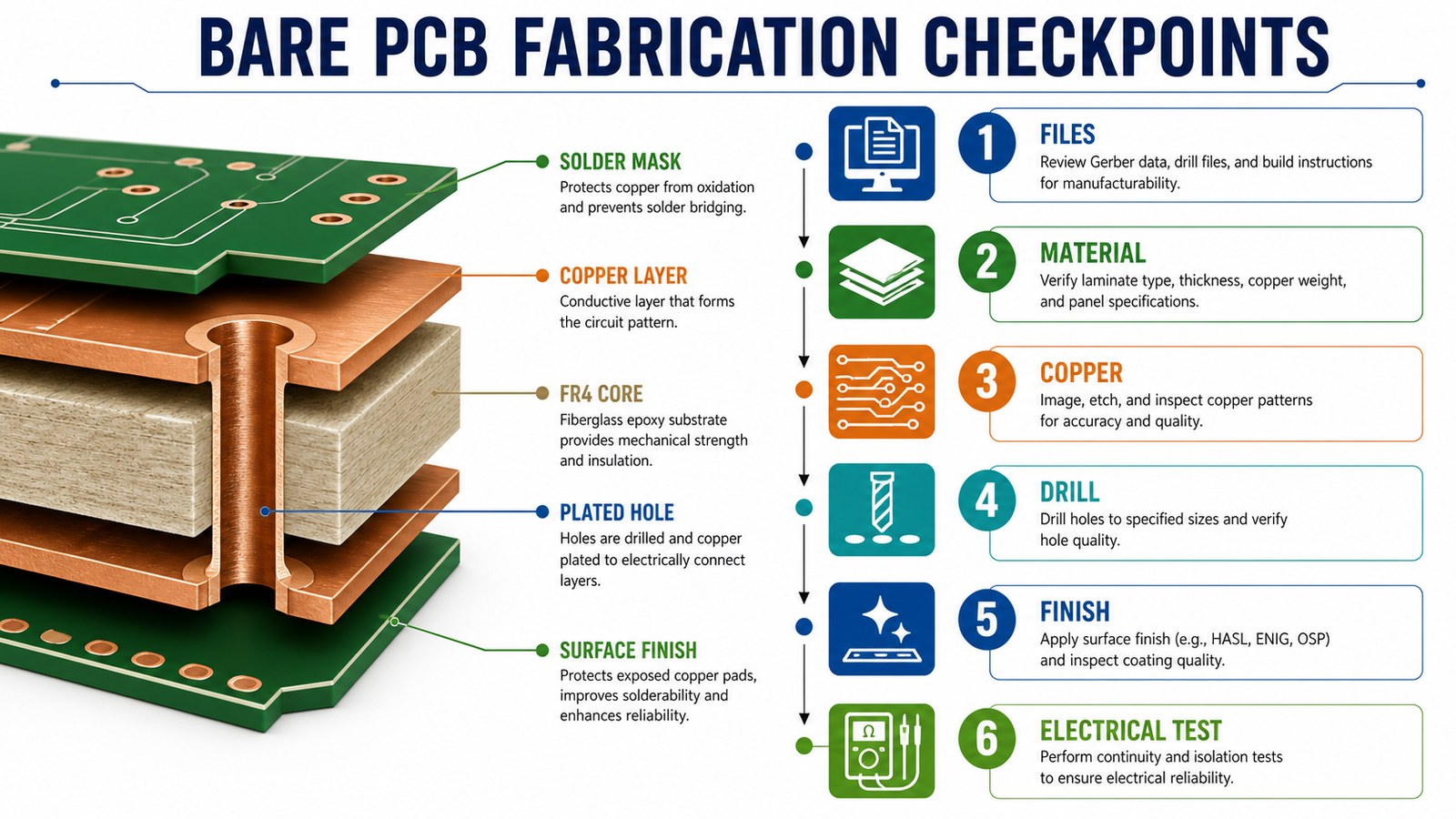
Microsection analysis exposes internal construction that cannot be assessed from a surface photograph. A prepared section can show the relationship between a plated hole, inner-layer copper and the surrounding laminate. That is valuable when the question concerns an interconnection inside the board rather than an exposed pad.
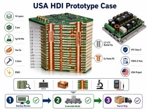
We provide microsection preparation and analysis and copper-thickness testing as part of our PCB testing capabilities. For our HDI boards, the question may involve a microvia interface or an interconnected via structure. The section location and represented construction therefore matter as much as the image itself.
The benefit for your project is evidence about an otherwise hidden feature. A section represents the sampled area; additional sampling or reliability evaluation may be needed for the application’s requirements. The illustration above explains the inspection concept and is not a production micrograph.
How Does Electrical Testing Complement Visual Inspection?
Electrical testing evaluates whether intended nets are connected and separate nets remain isolated under the test conditions. Visual inspection examines physical features. Together they address two different aspects of the bare board: its construction and its circuit connectivity.
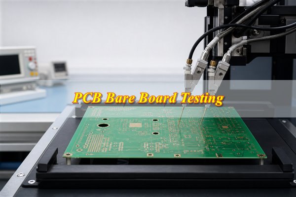
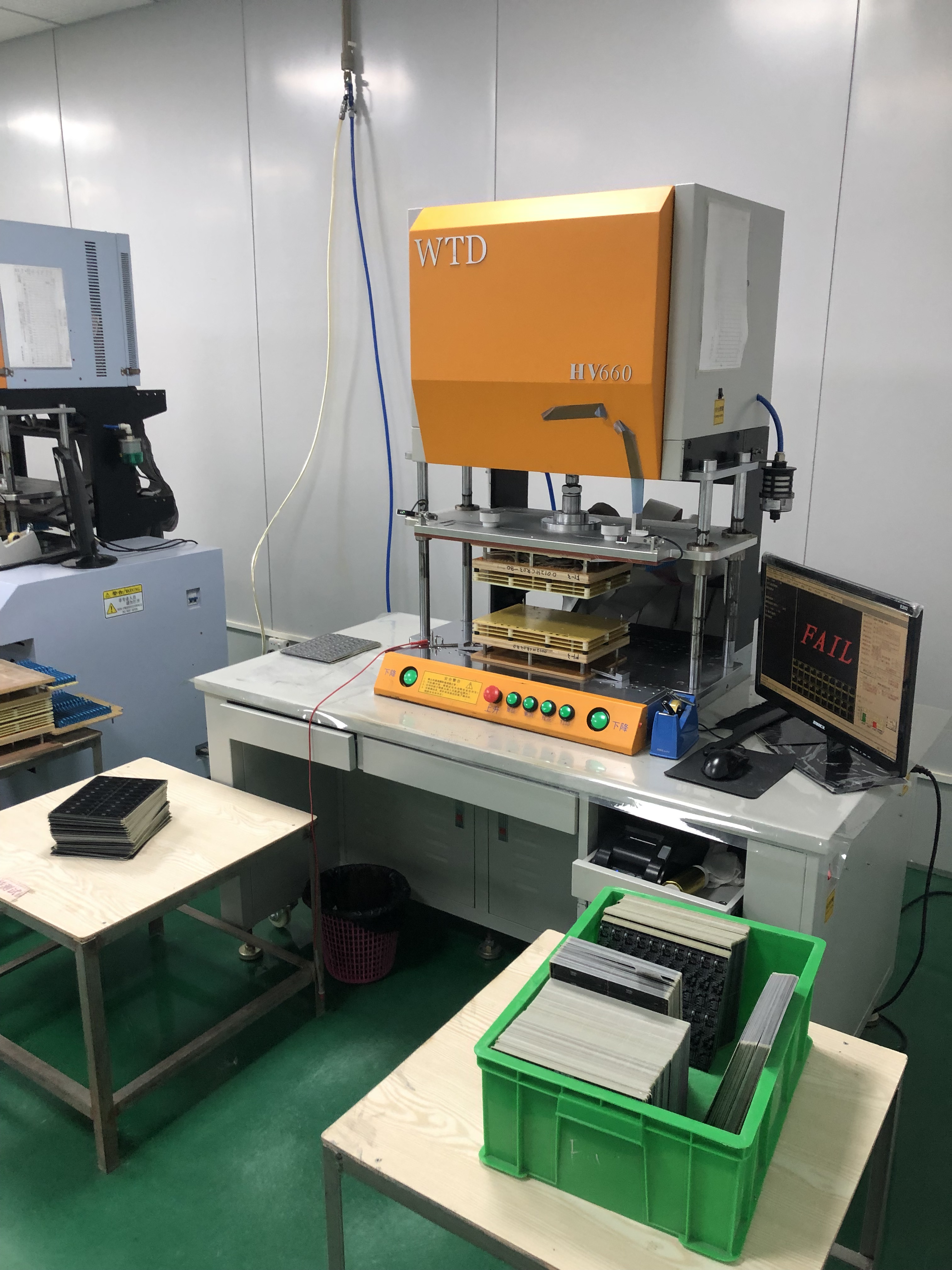
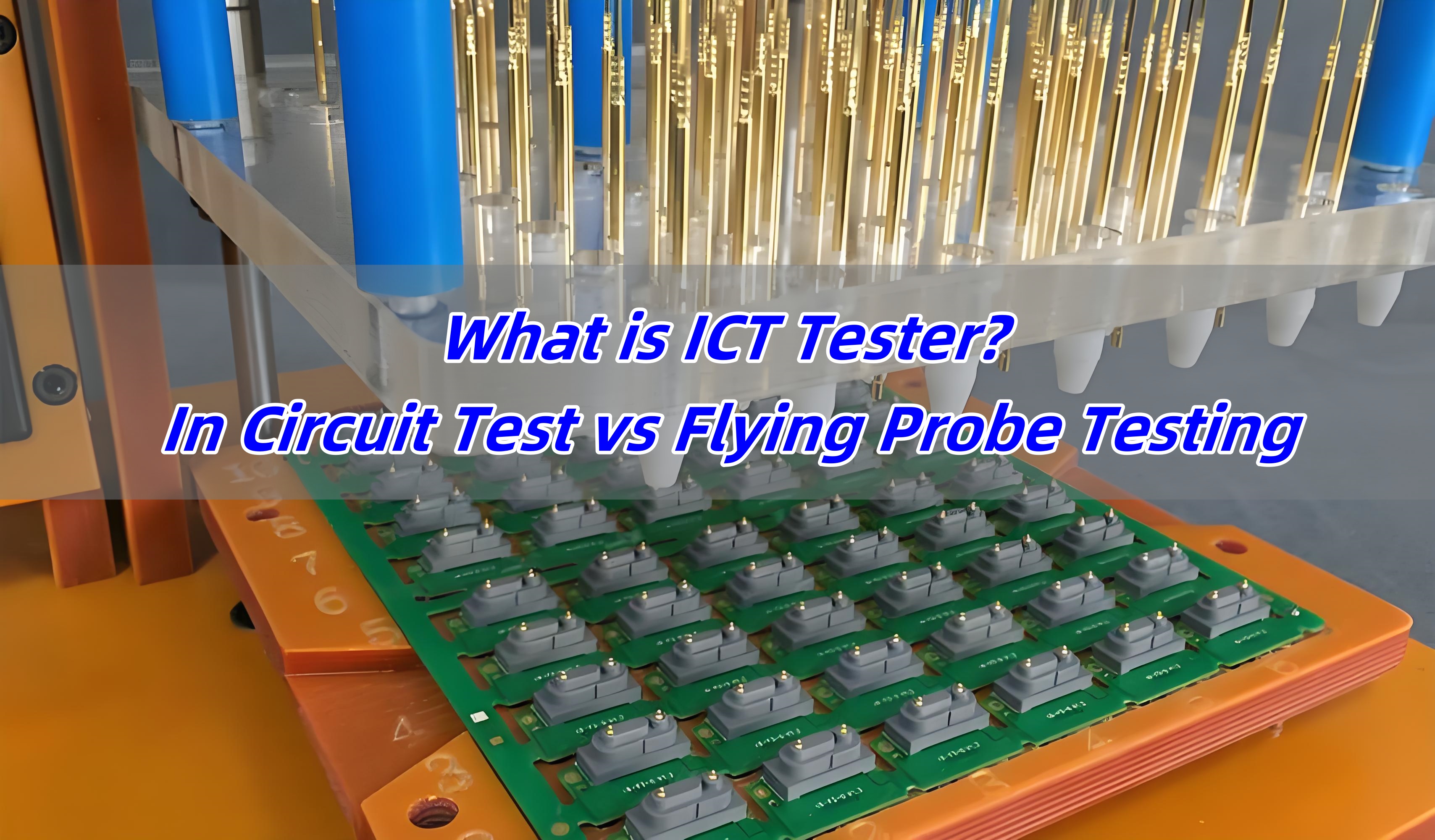
Our PCB testing capabilities include flying-probe testing, universal electrical testing and open/short testing. These are directly relevant to finding connectivity faults before components are added. A conductor pattern may appear complete yet contain an open connection; electrical testing addresses that question without relying on appearance alone.
For designs with controlled-impedance traces, we also provide impedance testing. This answers a different question from continuity: whether the specified transmission-line characteristic is achieved. The tests required for a particular board depend on its design and the agreed requirements; an electrical pass is not a substitute for every other specified evaluation.
Why Do Different PCB Constructions Need Different Checks?
Different constructions contain different interfaces and interconnections. The acceptance reference remains useful across them, but the features relevant to a two-layer rigid board are not identical to those in a multilayer HDI or rigid-flex design.
Coverlay openings, bonded regions and rigid-to-flex transitions
Electrical connections and the mechanical interfaces involved in installation or flexing.
Our FR4 manufacturing capability extends to 32 layers, subject to the stack-up, dimensions, materials and engineering review. As internal connections become more complex, the construction information becomes more important to selecting meaningful inspection evidence. This is why layer count alone is not enough to describe the board we are being asked to manufacture.
How Can Inspection Evidence Help Resolve a Board Concern?
A useful quality discussion connects the observed condition to the affected feature and its requirement. If you have a concern about a supplied board, we can review it with your part information, the location of the feature and the relevant photographs or measurements. That gives both teams a specific technical issue to discuss.
For example, a question about whether a lead will fit a hole calls for finished-hole dimensions and the component requirement. A concern about an internal connection may call for sectioning or electrical evidence instead. The benefit is a response directed at the actual board function, rather than a general judgment based on one photograph. Any proposed change to an agreed acceptance requirement needs customer agreement.
What Does IPC-A-600 Certification Mean for Customers?
IPC A 600 certification refers to personnel training and assessment credentials. It answers a question about knowledge of the standard, whereas inspection and test results answer questions about a particular board or lot. These are different forms of evidence.
For your project, the relevant discussion with us is the required board construction, acceptance basis and available inspection or testing support. Personnel credentials, when required, need separate confirmation of their scope and validity. A credential is not a replacement for evidence about the product being delivered.
How Can We Support Your Next PCB Build?
We combine custom PCB manufacturing, DFM engineering review and PCB testing support. This lets us discuss your acceptance requirements in the context of the actual board, from its stack-up and holes to its surface finish and assembly interfaces.
For an IPC-A-600 question about your next build, contact sales@bestpcbs.com with your fabrication data and the requirements already defined for the project. At EBest Circuit (Best Technology), we can review the design and discuss the applicable inspection and testing needs before manufacture.
PCB bare board testing verifies opens and shorts before assembly. It compares the electrical networks of an unpopulated printed circuit board with approved connectivity data before defects become harder and more expensive to isolate. A meaningful result must also identify the tested revision, coverage, limits, exclusions, traceability, and disposition rules.
A “passed” label is meaningful only when the method, source netlist, limits, exclusions, and report content are defined. Electrical verification does not replace visual, dimensional, impedance, cleanliness, solderability, or reliability controls.
What Is PCB Bare Board Testing?
PCB bare board testing verifies continuity and isolation. Continuity testing and isolation testing compare accessible conductive points with a reference derived from the released design. Net count, board density, via structures, access constraints, and special measurements determine test complexity.
The test is often called bare-board electrical test, E-test, continuity-and-isolation test, or netlist test. It can identify electrical opens and shorts, but it does not prove that every physical feature meets drawing requirements. It also does not guarantee that an assembled product will function. Visual workmanship, dimensions, copper and plating requirements, controlled impedance, solderability, cleanliness, and assembly performance remain separate verification activities.
Why Is Bare Board Testing Important Before PCB Assembly?
PCB bare board testing prevents known defects from entering assembly. Its value can be divided into four practical benefits:
Lower assembly loss: Detecting opens and shorts before component placement avoids wasting components, reflow capacity, inspection time, and troubleshooting labor.
Earlier defect containment: Testing close to PCB fabrication allows affected boards to be isolated before more value is added. This is especially useful for fine-pitch parts, buried connections, dense multilayers, and products that are difficult to probe after assembly.
Clear responsibility boundary: The PCB manufacturer can document the electrical condition at shipment, while the assembler controls handling, storage, assembly, and downstream testing.
Better purchase-order control: Defined coverage reduces disputes caused by vague language such as “electrically tested.” The order should identify the data revision, coverage level, acceptance basis, reporting needs, and special test conditions.
What Defects Can Bare Board Testing Detect?
PCB bare board testing finds electrical connectivity defects. The main results depend on test access, the approved program, and the specified measurement conditions:
Open circuits: PCB bare board testing detects interrupted nets caused by incomplete etching, cracked copper, failed via connections, annular-ring breakout, poor hole-wall metallization, or routing damage.
Short circuits: It detects unintended connections caused by copper bridges, conductive residue, imaging errors, plating anomalies, or incorrect fabrication data.
Intermittent connections: Unstable defects may require repeated measurements, thermal conditioning, resistance monitoring, microsectioning, or reliability testing.
Not covered by electrical testing: Visual defects, dimensional errors, impedance deviations, contamination, solder-mask registration, and material conditions require separate inspection or measurement.
Flying Probe vs Fixture Testing: Which Bare Board Testing Method Should You Choose?
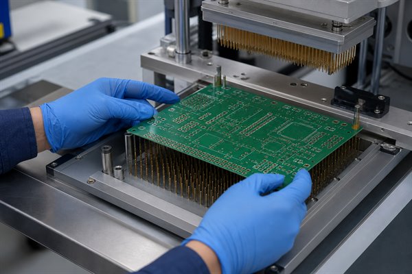
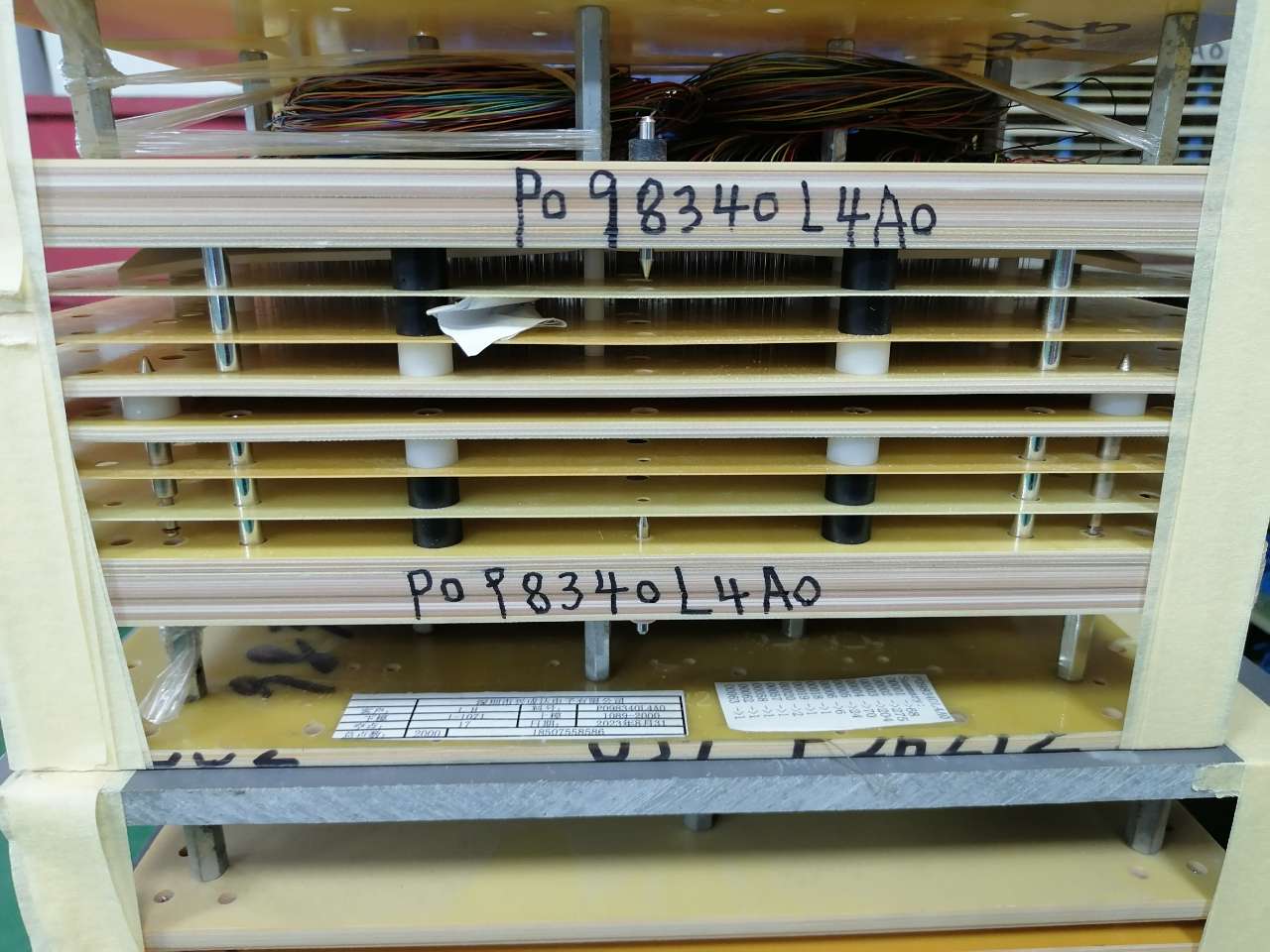
For PCB bare board testing, use flying probe testing for flexibility. Use fixture testing for throughput. The final choice depends on volume, revision stability, access, setup cost, and required test time.
Decision Factor
Flying Probe
Fixture Testing
Operating principle
Moving probes contact test points sequentially according to the test program
A dedicated adapter contacts many test points in parallel
Typical fit
Prototype, low volume, frequent revision
Stable design, medium-to-high volume
Dedicated tooling
Usually not required
Required and revision-specific
Setup profile
Program generation and validation
Fixture plus program generation and validation
Throughput
Sequential probing; often slower
Parallel contact; often faster after setup
Upfront cost
Lower because no dedicated fixture is normally needed
Higher because the fixture must be designed, built, and validated
Cost per board
Can remain higher as test time increases with point count
Can decrease across stable production volumes after setup
Revision response
Program changes may be sufficient
Fixture rework or replacement may be needed
Access risk
Probe reach, pad size, stability, and routing
Probe density, fixture mechanics, alignment, and wear
Board support
Requires stable positioning during probe movement
Requires uniform support and controlled pressure across the fixture
Maintenance
Probe condition, alignment, and program control
Probe wear, fixture cleaning, storage, alignment, and revision control
Special measurements
Flexible for selected points, low-resistance checks, or engineering investigation when equipment supports them
Suitable for repeatable production measurements when designed into the fixture and switching system
Primary limitation
Runtime increases with test-point count and measurement scope
Tooling cost and lead time are difficult to justify for changing designs
Best selection rule
Choose when flexibility and low setup commitment outweigh runtime
Choose when stable volume and throughput justify dedicated tooling
Which Board and Order Factors Affect Test-Method Selection?
Balance coverage risk, design stability, setup cost, and runtime. Review production quantity, expected repeat orders, board size, net and test-point count, pad geometry, layer count, via technology, panel format, and required measurements. A prototype likely to change favors flexible programming; a mature design produced repeatedly may justify a fixture whose preparation cost is distributed across more units.
Then examine what must be tested and what is physically accessible. Fine-pitch pads, solder-mask clearance, surface finish, board support, bow and twist, and probe force can affect contact reliability. Controlled-impedance verification, very low resistance, or elevated-voltage isolation may require methods beyond a basic continuity-and-isolation routine. The manufacturer should review unusual requirements before quotation so the chosen method, limits, tooling, report, and lead time are aligned.
How Does the PCB Bare Board Testing Process Work?
PCB bare board testing starts with controlled data. Confirm the released revision, reference netlist, accessible points, and approved limits before loading the board. The following eight steps create a traceable test and release process.
Review the order and data package. Confirm part number, revision, quantity, panelization, applicable drawings, test coverage, special nets, reporting, and acceptance requirements.
Create and compare the test reference. Generate connectivity from trusted design data and perform an independent comparison where required to reduce the risk of testing a fabrication error against the same erroneous source.
Prepare the program and access plan. Map test points, choose probe paths or fixture contacts, apply agreed limits, and identify intentionally untested or inaccessible points.
Validate setup. Check alignment, contact, board support, program revision, fixture identification, and known-reference behavior before production testing.
Run continuity and isolation checks. Test the required networks and capture failures with sufficient location information for diagnosis.
Confirm suspect results. Clean or inspect contact surfaces, repeat the measurement under controlled rules, and distinguish contact instability from a repeatable board defect.
Control nonconforming boards. Segregate failures, record disposition, control any repair or retest authorization, and preserve traceability.
Release records. Link the test status and report to the correct lot, date, equipment or program, and approved product revision.
Which Standards Apply to PCB Bare Board Testing?
PCB bare board testing standards must be named by revision. IPC-9252B addresses test data, parameters, equipment, and fixturing for unpopulated boards. IPC’s current revision table marks IPC-9252 as no longer maintained. The purchase order should therefore identify the accepted revision or an agreed alternative. Its scope is conductive-network verification, not every physical, material, dimensional, or assembly requirement.
IPC-A-600 addresses externally and internally observable acceptability conditions; IPC’s revision table listed IPC-A-600M in May 2025. The applicable IPC-6010-series performance specification and procurement documentation define requirements for the relevant board type and class. Drawings, purchase orders, approved deviations, and sector-specific requirements may add controls, so the contract should state document revisions and order of precedence.
High-voltage, aerospace, medical, automotive, or other high-reliability applications may demand additional validation, records, or process controls. Those requirements should be specified by the responsible design authority. A supplier should not infer a hipot voltage, insulation criterion, test class, or sampling permission from the product description alone.
What Files Are Needed for PCB Bare Board Testing?
The test package must identify the product and test reference. Provide the following controlled files and instructions:
Fabrication data: Supply the released Gerber or ODB++ package with clear layer identification.
Drill data: Include plated and non-plated drill files plus any required drill drawing or tool information.
Product identification: State the part number, fabrication revision, board or panel drawing, quantity, and panelization requirements.
Reference netlist: Provide IPC-D-356 or trusted CAD-derived connectivity data when an independent electrical reference is required. If the netlist is extracted from fabrication files, define how it is generated and compared.
Test requirements: Define coverage, continuity and isolation limits, inaccessible points, no-probe areas, and any special measurement conditions.
Special structures: Identify net ties, intentionally connected planes, embedded components, isolated copper, edge contacts, castellations, coupons, and controlled-impedance requirements.
Reporting instructions: Specify lot- or serial-level reporting and whether the deliverable must include a certificate, summary, raw measurements, or failure map.
Data-control rules: Define secure transfer, authorized access, retention, and deletion requirements for commercially sensitive design files.
100% Netlist Testing vs Optimized Testing vs Sampling
These three coverage models are not interchangeable. The order must define the tested units, program scope, exclusions, and approval basis rather than relying on a short coverage label.
Coverage Model
Meaning to Confirm
Procurement Control
100% netlist test
Every production board runs the defined electrical program; this does not mean every physical feature is measured
Define accessible nodes, program scope, exclusions, and lot traceability
Optimized test
The program reduces redundant contacts or sequences while preserving the agreed network verification
Approve the optimization basis, retained coverage, and excluded points
Sampling
Only units selected by the approved sampling plan are tested; other boards remain untested
State the sample size, selection method, acceptance rule, risk basis, and authorization
Sampling must not replace contracted every-board testing. Any change requires written authorization under the applicable specification and risk assessment.
What Are the Acceptance Criteria for Bare PCB Testing?
Acceptance criteria must turn “pass” into measurable rules. Define the following items before program approval and production testing:
Continuity limit: State the maximum permitted resistance for an intended net, using values appropriate to trace length, conductor geometry, connectors, planes, and low-resistance paths.
Isolation limit: Define the minimum resistance or maximum leakage allowed between separate nets. High-voltage products may require different limits and test conditions from routine circuitry.
Coverage: Specify whether every board, an optimized net set, or an approved sample is tested. Identify inaccessible points, excluded features, and permitted optimization.
Special measurements: For hipot, four-wire resistance, or other special checks, define voltage, current, dwell time, temperature, measurement method, test location, and guarding requirements.
Data identity: Link acceptance to the correct part number, fabrication revision, controlled netlist or checksum, test-program revision, and approved change record.
Failure confirmation: Define how contact instability is distinguished from a repeatable board defect and which controlled measurements may be repeated.
Repair and retest: State whether repair is permitted, who can authorize it, which workmanship rules apply, and whether the affected net or complete program must be rerun.
Required evidence: Define the certificate, test summary, failure map, raw results, traceability fields, and record-retention period required for acceptance.
Do not apply one generic limit to every design. Electrical limits must follow the product’s design intent, governing specification, and confirmed test feasibility.
What Should a Bare Board Test Report Include?
A useful report must link results to the delivered boards. Specify the required report level in the purchase order:
Product identity: Customer part number, fabrication revision, lot or work order, and panel or serial identification when required.
Test quantity: Quantity received, tested, passed, failed, repaired, retested, and finally released.
Coverage: Every-board, optimized, or sampling status plus inaccessible points and approved exclusions.
Test method: Flying probe, fixture, or other approved method, including program and fixture identification.
Acceptance settings: Continuity and isolation limits plus voltage, current, dwell time, or other special conditions when applicable.
Equipment control: Tester identification and calibration-status reference when contractually required.
Failure history: First-pass failures, confirmed defects, retest results, repair status, and final disposition.
Authorization: Test date, operator or approval record, applicable specification, and acceptance basis.
Record control: Report format, lot or serial linkage, retention period, and retrieval requirements.
A certificate is not the same as a detailed test report. Name the exact deliverable required before production begins.
What Causes False Failures in Bare Board Testing?
False failures usually come from contact, setup, or data errors. False failures in flying probe testing and fixture testing should be checked before a board is classified as defective:
Contaminated contact surfaces: Oxidation, residue, debris, or surface-finish variation can increase or destabilize contact resistance.
Restricted probe access: Small pads, solder-mask encroachment, or unsuitable no-probe geometry can prevent reliable contact.
Probe condition: Worn, dirty, damaged, or incorrectly selected probes can produce unstable readings.
Force and alignment: Incorrect probe force, fixture alignment, fiducial recognition, or board positioning can move contact away from the target.
Board support: Bow, twist, movement, or inadequate support can prevent uniform fixture contact or allow a thin board to flex.
Incorrect test data: A Gerber and netlist revision mismatch, wrong layer polarity, misunderstood net tie, isolated-copper definition, or incorrect drill file can create systematic false failures.
Fixture or program control: Worn fixture contacts, an unvalidated program change, or mismatched fixture identification can affect repeated production tests.
Preserve the original result before retesting. Correct only a verified contact or setup issue, rerun the defined scope, and record both outcomes.
How Should Failed Boards and Retests Be Controlled?
Confirmed failures must be segregated and traceable. The record should retain board or panel identity, failed net or point information, failure type, test program, date, and investigation status. This prevents accidental mixing and gives process engineering enough evidence to search for recurring patterns across panel position, layer, drill tool, plating batch, or routing operation.
Retest rules should distinguish contact confirmation from a disposition-changing retest. Cleaning a pad and repeating an unstable contact may be legitimate when the original result is retained. A repeatable open or short requires nonconformance control. Permitted repairs need authorization, workmanship criteria, inspection, retesting of the complete affected scope, and traceability. Authorized personnel must approve scrap, use-as-is, or deviation decisions.
What Affects PCB Bare Board Testing Cost and Lead Time?
Cost and lead time depend on setup, runtime, and reporting. The main drivers are:
Order quantity: Low volumes often favor flying probe; stable repeated volumes may justify dedicated fixture cost.
Net and point count: More nodes, dense access, and complex connectivity increase programming and test time.
Board and panel format: Large panels, thin boards, unusual outlines, and difficult support conditions can require additional handling or tooling.
Test method: Flying probe reduces dedicated tooling but may increase runtime; fixture testing adds preparation cost but improves throughput after validation.
Revision stability: Design or panel changes may require program revalidation, fixture modification, or replacement.
Special measurements: Hipot, four-wire resistance, controlled-impedance reporting, or custom limits may require engineering review and additional setup.
Traceability and reports: Serial-level records, raw measurements, failure maps, or customized reports add data-handling and review time.
Input completeness: Missing files, conflicting revisions, undefined limits, or late requirement changes delay program approval and quotation.
Release a complete, stable test package at quotation. This is the most effective way to reduce avoidable setup cost and schedule delay.
PCB Bare Board Testing Checklist
Resolve coverage and reporting decisions before order release. This PCB bare board testing checklist captures the requirements that materially change risk, documentation, or delivery. Not every item applies to every PCB, but each omission should be a deliberate engineering or procurement decision rather than an assumption.
Product identity: Confirm the customer part number, fabrication revision, and approved data set.
Coverage model: State whether every board, an optimized net set, or a defined sample is tested.
Test method: Identify the required method or allow the manufacturer to propose flying probe or fixture testing.
Electrical limits: Define continuity, isolation, and any special measurement conditions.
Reference netlist: Provide an independent netlist when required and define how data comparison is controlled.
Special structures: Identify net ties, embedded parts, isolated copper, coupons, edge contacts, and no-probe areas.
Physical access: Confirm test access, solder-mask clearance, surface finish, support, and warp expectations.
Applicable documents: Name the governing standards, revisions, performance class, drawings, and order of precedence.
Traceability: Specify lot, panel, or serial traceability and record-retention period.
Deliverables: List the required certificate, summary report, failure map, or raw results.
Data security: Agree secure file-transfer and design-data retention requirements.
Fixture control: Confirm ownership, storage, maintenance, and revision compatibility when applicable.
Separate inspections: Define visual, dimensional, impedance, cleanliness, solderability, and reliability requirements independently.
FAQs About PCB Bare Board Testing
Q1: Can bare board electrical testing verify controlled impedance?
A1: No. Standard continuity and isolation do not measure impedance. Impedance verification normally uses designated test coupons or an agreed trace-measurement method with separate limits and records. A board can pass the electrical net test while an impedance structure is outside tolerance, so the drawing and purchase order should state both requirements independently.
Q2: When is four-wire or Kelvin resistance measurement needed?
A2: Use it when probe and lead resistance could distort results. It may be relevant to heavy-current paths, low-resistance structures, or other critical nets, but it is not automatically included in a standard opens-and-shorts program. Define the target locations, limits, current, method, and reporting conditions before quotation.
Q3: Why can a PCB pass bare-board testing but fail after assembly?
A3: Bare-board testing verifies connectivity, not assembled function. Reflow can expose marginal vias, handling can damage the board, and assembly can introduce soldering or component defects. A clean bare-board result therefore does not replace AOI, X-ray where applicable, ICT, functional testing, or investigation of defects that appear only after thermal or mechanical stress.
Q4: Are flying-probe contact marks acceptable on finished pads?
A4: Controlled probe marks are not automatically damage. Acceptability depends on pad geometry, finish, probe type, force, location, and the applicable product requirements. Gold fingers, wire-bond pads, press-fit areas, or cosmetically controlled contacts may require no-probe zones or an approved contact method.
Q5: Should I supply a netlist or let the fabricator generate one from Gerber data?
A5: Supply an independent netlist when design-intent comparison matters. A fabricator can extract connectivity from Gerber and drill data, but that reference may reproduce the same output error. An IPC-D-356 or trusted CAD-derived netlist allows comparison between design intent and fabrication data. State the approved revision and how mismatches must be resolved.
Q6: Does “electrically tested” mean every accessible node was checked?
A6: Not unless the contracted coverage says so. Some programs verify only selected or optimized points, while an independent netlist may support broader node-level comparison. Ask whether every board was tested, which nodes were accessible, what optimization was used, and which points or structures were excluded. The report should use the same coverage definition as the purchase order.
Q7: Should test points remain on a PCB after the prototype stage?
A7: Keep the access needed for production test and diagnosis. Removing prototype test points can make fixture testing, troubleshooting, and failure confirmation harder. Retain accessible points for critical nets when space permits, and coordinate pad size, spacing, side, keepout, finish, and probe restrictions with the intended test method before the layout is released.
Q8: What makes a PCB test point reliable for probe or fixture contact?
A8: Reliable access needs suitable geometry and mechanical support. Pad size, center spacing, solder-mask clearance, surface condition, probe-tip selection, board alignment, and support all affect contact stability. Dense layouts may require a fabricator or fixture review because a test point that is electrically valid can still be difficult to contact repeatedly.
Q9: Can PCB bare board testing find intermittent microvia defects?
A9: A standard test can miss a temporarily stable connection. Repeated probing, controlled flexing, thermal conditioning, resistance monitoring, microsectioning, or reliability testing may be needed when the failure mechanism warrants it. The investigation method should follow the defect evidence and product requirements rather than an automatic retest routine.
Q10: How should a failed board be identified within a production panel?
A10: Use an agreed mark linked to the panel test record. A failed unit may be physically marked, mapped by panel position, or tracked electronically, depending on the assembly and depanelization process. The method must prevent an X-out or failed position from entering assembly and must preserve the original failure, retest, repair, and disposition history.
Request your PCB bare board testing quotation from BestPCBs. Send the released fabrication data, approved netlist, quantity, revision, coverage, acceptance criteria, and report format to sales@bestpcbs.com. Our engineering team will review the test requirements and provide a manufacturing quotation for prototypes, volume production, OEM, ODM, or custom PCB projects.
A bare PCB manufacturer fabricates unpopulated printed circuit boards and verifies the board before components are mounted. For buyers, the important decision is not only who can make the board, but who can check the Gerber files, material, copper, holes, surface finish, solder mask, test plan and quote assumptions before production starts.
EBest Circuit supports bare PCB projects from file review through fabrication, electrical test and later PCBA support when the same design needs assembly after the board is approved. This article explains what to check before choosing a bare PCB manufacturer and what to send for a practical RFQ.
What can go wrong when a bare PCB order is treated as a simple board purchase?
Many bare board problems appear before assembly, but buyers often discover them only when components are already waiting.
Gerber, drill, stackup and drawing files do not describe the same revision, causing quote assumptions to drift.
Material, Tg, board thickness, copper weight or surface finish is selected without checking manufacturability.
Fine line, spacing, hole size, solder mask bridge or outline tolerance is pushed too close to the process limit.
The buyer orders bare boards first, then discovers assembly, stencil, fixture or test needs were not considered.
Electrical test, impedance, panelization or packaging requirements are not stated clearly enough for production.
EBest Circuit helps buyers turn bare PCB files into a controlled manufacturing package.
We review Gerber or ODB++ files, drill data, stackup, copper, board thickness, surface finish and solder mask requirements before quote assumptions are locked.
We can discuss FR4 low Tg, mid Tg and high Tg material routes, including when a high Tg or higher-layer design needs extra review.
We check common manufacturability items such as 4/4mil line and spacing, finished hole size, through-hole aspect ratio, solder mask bridge, panelization and test needs.
We connect bare PCB fabrication with assembly planning when the buyer also needs BOM, CPL, stencil, component sourcing, inspection or functional test support.
We keep quote questions visible early, so buyers can compare suppliers by risk, not only by unit board price.
What a Bare PCB Manufacturer Should Deliver
A bare PCB manufacturer should deliver manufacturable boards that match the released files and are ready for assembly, testing or product validation.
A useful supplier does more than image copper and ship boards. It should review file completeness, stackup, laminate, copper weight, drill data, solder mask, silkscreen, surface finish, outline, panelization and electrical test requirements. For FR4 projects, buyers can also compare whether the supplier can support the material and process route shown in the design, such as standard FR4 PCB, high Tg FR4, heavier copper or tighter spacing.
Is a Bare PCB the Right Order Type for Your Project?
A bare PCB order is right when you need fabricated boards without mounted components, or when you want to approve the board before assembly starts.
Project Situation
Order Fit
Buyer Check
Design validation before component build
Bare PCB can fit well
Confirm test coupons, dimensions and finish
Buyer has an assembly partner already
Bare PCB is often enough
Share assembly constraints before fabrication
Prototype then PCBA later
Bare PCB first, PCBA later
Keep BOM, CPL and stencil needs visible early
Turnkey electronic product build
PCBA or turnkey route may fit better
Quote board and assembly together
Bare PCB vs PCB Assembly: What Buyers Should Separate
Bare PCB manufacturing makes the unpopulated board; PCB assembly mounts and solders components onto that board.
Separating these scopes helps avoid unclear quotes. Bare PCB questions include material, layer count, copper, holes, surface finish and electrical test. Assembly questions include BOM, CPL, stencil, polarity, package size, soldering method, inspection and functional test. If the same project will later move into assembly, connect the bare board review with the PCB manufacturing and assembly plan early.
Bare PCB Manufacturing Capabilities at a Glance
Capability should be checked against the exact design, but a useful RFQ can start from material, layer count, copper, thickness, holes, line width and surface finish.
Capability Area
Verified Example
RFQ Note
Material
FR4 low Tg, mid Tg and high Tg routes listed
Confirm laminate and Tg with the design environment
Layer count
FR4 high Tg common range includes 1-10 layers
Higher layer counts require project review
Copper
Inner HOZ-5OZ and outer 1OZ-5OZ listed as common ranges
Heavier copper affects spacing, etching and cost
Finished hole
0.2mm common example; 0.15mm special review route
Check annular ring, aspect ratio and tolerance
Line width / spacing
4/4mil common examples; 3/3mil special route
Do not quote tight designs without DFM review
Surface treatment
OSP, HASL, ENIG, immersion silver, immersion tin, ENEPIG and hard gold options listed
Choose around assembly, storage and reliability needs
What Can Go Wrong Before Components Are Mounted
Bare board defects can block assembly even when no components have been placed yet.
Common risks include wrong revision files, missing drill data, copper spacing that cannot support the requested copper weight, solder mask openings that affect pads, unclear impedance or electrical test requirements, board outline issues, and surface finish choices that do not match storage or soldering needs. The earlier these are reviewed, the easier it is to fix them before production cost is committed.
How EBest Circuit Helps Buyers Control Bare PCB Risk
EBest Circuit helps by checking manufacturing details before the buyer treats the quote as final.
Send the Gerber or ODB++ files, drill files, stackup, drawing, board thickness, copper, surface finish, quantity and inspection needs. If the board will later become an assembled product, send BOM and CPL as well so fabrication decisions do not create avoidable assembly problems.
Materials, Layer Count and Board Thickness
Material and thickness decisions should match electrical, mechanical, thermal and assembly requirements.
FR4 is common for many bare PCB projects, but Tg grade, laminate family, prepreg, layer count and finished thickness still matter. The verified capability source lists FR4 low Tg, mid Tg and high Tg material routes, with higher-layer or special material designs requiring review. Finished thickness also depends on the process and surface finish route, so buyers should not send only a board outline and expect a complete quote.
Copper Weight, Line Width, Spacing and Hole Design
Copper and drill choices should be checked together because one change can affect spacing, plating, cost and reliability.
For common FR4 routes, the capability source lists inner copper examples from HOZ to 5OZ and outer copper examples from 1OZ to 5OZ, with heavier copper requiring review. It also lists 4/4mil line width and spacing as common examples and 3/3mil as a special review route. Buyers should send copper weight, current requirements, minimum trace/space, finished hole size and tolerance expectations together.
Surface Finish, Solder Mask and Silkscreen Choices
Surface finish, solder mask and silkscreen choices affect solderability, inspection, storage and assembly readiness.
Common surface treatment options include OSP, HASL, ENIG, immersion silver, immersion tin, ENEPIG and hard gold fingers. Solder mask color can also matter when optical inspection, LED reflection, branding or contrast is important. The RFQ should state the preferred finish, mask color, legend requirements and any storage or assembly constraints.
Bare PCB Fabrication Process
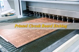
The bare PCB fabrication process should move from file review to material preparation, imaging, etching, drilling, plating, solder mask, surface finish and final inspection.
The useful question for buyers is not only the order of steps. It is where each step can change the result. Material choice affects stackup. Copper affects etching and spacing. Drilling affects plating and reliability. Surface finish affects solderability. Electrical test confirms open and short risk before the bare boards move to assembly.
Testing and Inspection Before Shipment
Bare PCB testing should confirm that the unpopulated board is electrically and visually ready for the next build stage.
Depending on the design, inspection may include visual checks, AOI, dimensional checks, solder mask checks, electrical test, impedance review or sample-level confirmation. Buyers should specify whether every board needs electrical test, whether test reports are required and whether packaging must protect the board finish for later assembly.
Cost Factors for Bare PCB Manufacturing
Bare PCB cost changes with material, layer count, copper, board size, hole density, surface finish, tolerance, test and quantity.
Cost Factor
Why It Matters
What to Send
Material and Tg
Changes laminate cost and process route
Laminate preference or operating requirement
Layer count
Changes lamination and drilling complexity
Stackup and impedance needs
Copper weight
Affects etching, spacing and plating
Inner and outer copper requirements
Surface finish
Affects solderability and shelf life
OSP, HASL, ENIG or other finish preference
Testing
Adds inspection work and reduces shipment risk
Electrical test, impedance or report needs
Prototype, Low-Volume and Production Order Planning
Prototype and production bare PCB orders should be planned differently because the risk is not always the same.
Prototype orders often need fast DFM feedback, revision control and clear questions before the design is released. Production orders need stable specifications, panelization, repeatable test requirements, packaging and supplier communication. If the design will later require mounted parts, use early board feedback to prepare the later prototype PCB assembly or production assembly route.
How to Evaluate a Bare PCB Manufacturer
A bare PCB manufacturer should be evaluated by DFM response, capability fit, file discipline, testing clarity and communication quality.
Does the supplier ask clear questions before quoting unclear files?
Can it support the material, copper, line width, spacing, hole and thickness requirements?
Does it explain when a requirement needs special review instead of silently accepting it?
Can it connect bare board fabrication with later assembly planning when needed?
Does the quote state surface finish, testing, quantity, revision and delivery assumptions clearly?
RFQ Checklist for Bare PCB Manufacturing
A useful bare PCB RFQ should include the files and constraints that affect manufacturability, price and shipment risk.
Gerber or ODB++ files, drill files and fabrication drawing
Stackup, layer count, material, Tg requirement and board thickness
Copper weight, minimum line width/spacing, finished hole size and tolerance needs
Surface finish, solder mask color, silkscreen and special process requirements
Quantity, revision, panelization preference, electrical test and inspection report needs
BOM, CPL and assembly drawing if later PCBA support is required
FAQ About Bare PCB Manufacturers
What is a bare PCB manufacturer?
A bare PCB manufacturer fabricates unpopulated printed circuit boards before components are mounted. The work usually includes material preparation, copper patterning, drilling, plating, solder mask, surface finish, routing and electrical test.
Is a bare PCB the same as a PCB assembly?
No. A bare PCB is the circuit board without components. PCB assembly, or PCBA, mounts and solders components onto that board. Some buyers order bare boards only, while others need board fabrication plus assembly.
What files are needed for a bare PCB quote?
Send Gerber or ODB++ files, drill files, fabrication drawing, stackup, material, copper weight, board thickness, surface finish, quantity and test requirements. Add BOM and CPL if assembly planning is also needed.
Can EBest Circuit support bare PCB and later assembly?
Yes. EBest Circuit can review bare PCB manufacturability and also connect the build with component sourcing, assembly, inspection and test planning when the project needs PCBA support after board fabrication.
Need a bare PCB manufacturer for prototypes, low-volume builds or production orders? Send your Gerber or ODB++ files, drill files, stackup, material, copper, surface finish, quantity, test requirements and any later BOM/CPL needs to sales@bestpcbs.com. EBest Circuit can review DFM, fabrication risk, quote assumptions and assembly planning before production starts.
Struggling with bare PCB manufacturing delays, hidden costs, or quality inconsistencies? This guide reveals from process optimization to vendor selection, helping you achieve reliable, cost-effective boards with full traceability.
EBest Circuit (Best Technology) delivers precision-engineered bare PCBs with unmatched speed and reliability. Our advanced manufacturing capabilities support 2-36 layer boards with tight tolerances (±3% impedance control, 3/3mil trace/spacing), backed by 100% electrical testing and free DFM analysis to eliminate costly errors. We offer 24-hour rapid sampling with a 99.2% on-time delivery rate—50% faster than industry averages. Unlike suppliers with hidden fees, we provide transparent pricing (verified by 1,200+ clients in 2024) and dedicated 1-on-1 engineering support to optimize your designs for cost-efficiency.
With ISO-9001 and IATF 16949 certified production lines, we reduce defects to <0.5% versus the 2-3% industry standard. Whether you require HDI, rigid-flex, or high-frequency boards, our 24/7 responsive team ensures seamless transitions from design to mass production. Let’s discuss how our quality-first approach, accelerated timelines, and fair pricing can streamline your PCB supply chain. Contact us now: sales@bestpcbs.com.
What Is Bare PCB?
A bare PCB (Printed Circuit Board) refers to the unfinished foundational board that mechanically supports and electrically connects electronic components using conductive pathways, tracks, or signal traces etched from copper sheets. Unlike assembled PCBs, these lack soldered components, conformal coating, or final finishes, essentially serving as the raw platform for subsequent manufacturing stages. Manufactured through processes like imaging, etching, drilling, and plating, bare PCBs vary from single-layer designs to complex multilayered structures with blind/buried vias. Their quality directly impacts end-product reliability, with factors like material selection (FR-4, Rogers, or metal-core), trace precision, and impedance control determining performance in applications ranging from consumer electronics to aerospace systems.
What Is Bare PCB Manufacturing Process?
Here’s a structured breakdown of thebare PCB manufacturing process, written for practical reference without promotional language:
1. Design & File Preparation
Engineers finalize schematics and convert them into Gerber/ODB++ files, including drill maps and layer alignment data.
2. Material Selection
Substrates (FR-4, Rogers, etc.) are chosen based on thermal, mechanical, and electrical requirements.
3. Inner Layer Imaging
Copper-clad laminates are coated with photoresist, exposed to UV light through the design pattern, and etched to form conductive traces.
4. Oxidation & Lamination
Inner layers are oxidized for adhesion, stacked with prepreg, and pressed under heat to create multilayer boards.
5. Drilling
Precision CNC machines drill holes for vias and component leads, with tolerances as tight as ±0.05mm.
6. Plating & Metallization
Holes are electroplated with copper to establish electrical connections between layers.
7. Outer Layer Patterning
Similar to inner layers, outer copper is etched to finalize surface circuitry, often with added solder mask alignment.
8. Solder Mask Application
A protective epoxy layer is applied, leaving only solderable areas exposed, then cured under UV.
9. Surface Finishing
ENIG, HASL, or OSP coatings are added to prevent oxidation and ensure solderability.
What Are the Factors Affecting the Reliability of Bare PCB Manufacturing?
Here are the primary factors impacting reliability in bare PCB manufacturing:
Design for Manufacturability (DFM) Compliance: Overlooking automated assembly requirements like board size limits, panelization efficiency, or trace/spacing rules leads to rejection, manual handling, extended cycles, and higher costs.
Material Properties: Substrate thermal expansion coefficient mismatch with components induces stress cracks during thermal cycling. Copper foil roughness directly increases signal loss, especially at high frequencies, while inadequate thermal conductivity causes localized overheating.
Fabrication Process Control: Inconsistent etching causes undercuts or shorts. Drill misalignment or smear creates unreliable vias. Poor plating uniformity (thin spots, voids) weakens interconnects and increases resistance.
Impedance Control Accuracy: Variations in dielectric thickness, copper roughness, and trace geometry distort signals in high-speed designs, causing timing errors or data corruption.
Multilayer Lamination Quality: Layer misalignment during bonding breaks connectivity. Inadequate resin fill or voids between layers create delamination sites under thermal stress.
Thermal Management Design: High power density combined with limited copper thickness and thin substrates creates hotspots, accelerating component failure and board warpage.
Moisture and Contamination Resistance: Absorbed humidity vaporizes during soldering, causing internal blistering or layer separation. Chemical residues or pollutants corrode copper traces over time.
Surface Finish Integrity: Oxidation or poor solderability of finishes (e.g., ENIG, HASL) results in weak solder joints (voids, cold solder) prone to cracking. Inconsistent thickness reduces shelf life.
Benefit: Maintains ±5% measurement accuracy across tools.
Train Operators on Traceability Protocols
Require daily scans of material reels and tooling IDs.
Gamify compliance with leaderboards and performance bonuses.
Benefit: Achieves 99%+ scan adherence in 4–6 weeks.
Conclusion
Bare PCB manufacturing demands precision across design, material selection, and production processes to avoid impedance mismatches, etching defects, and layer misalignment. EBest Circuit (Best Technology) delivers reliable solutions with 18+ years of expertise, combining free DFM analysis to prevent 90% of pre-production errors and automated traceability systems for real-time quality tracking. Our vertically integrated supply chain reduces costs by 15-30% while maintaining IPC Class 3 standards, supported by a 24-hour engineering team to accelerate delivery without quality compromise. For high-performance bare PCBs with guaranteed signal integrity and on-time delivery, request your competitive quote today at sales@bestpcbs.com.
This website uses cookies to enhance your experience, remember your preferences, and help us understand how visitors use our site. You can accept all cookies, reject non-essential cookies, or manage your settings.
This website uses cookies to improve your experience while you navigate through the website. Out of these cookies, the cookies that are categorized as necessary are stored on your browser as they are essential for the working of basic functionalities of the website. We also use third-party cookies that help us analyze and understand how you use this website. These cookies will be stored in your browser only with your consent. You also have the option to opt-out of these cookies. But opting out of some of these cookies may have an effect on your browsing experience.
Necessary cookies are absolutely essential for the website to function properly. These cookies ensure basic functionalities and security features of the website, anonymously.
Cookie
Duration
Description
cookielawinfo-checkbox-analytics
11 months
This cookie is set by GDPR Cookie Consent plugin. The cookie is used to store the user consent for the cookies in the category "Analytics".
cookielawinfo-checkbox-functional
11 months
The cookie is set by GDPR cookie consent to record the user consent for the cookies in the category "Functional".
cookielawinfo-checkbox-necessary
11 months
This cookie is set by GDPR Cookie Consent plugin. The cookies is used to store the user consent for the cookies in the category "Necessary".
cookielawinfo-checkbox-others
11 months
This cookie is set by GDPR Cookie Consent plugin. The cookie is used to store the user consent for the cookies in the category "Other.
cookielawinfo-checkbox-performance
11 months
This cookie is set by GDPR Cookie Consent plugin. The cookie is used to store the user consent for the cookies in the category "Performance".
viewed_cookie_policy
11 months
The cookie is set by the GDPR Cookie Consent plugin and is used to store whether or not user has consented to the use of cookies. It does not store any personal data.
Functional cookies help to perform certain functionalities like sharing the content of the website on social media platforms, collect feedbacks, and other third-party features.
Performance cookies are used to understand and analyze the key performance indexes of the website which helps in delivering a better user experience for the visitors.
Analytical cookies are used to understand how visitors interact with the website. These cookies help provide information on metrics the number of visitors, bounce rate, traffic source, etc.
Advertisement cookies are used to provide visitors with relevant ads and marketing campaigns. These cookies track visitors across websites and collect information to provide customized ads.