Best practices for reducing PCB defects in manufacturing work when design requirements, production inputs, process limits, inspection coverage, and corrective action operate as one control system. Final inspection can contain a visible defect, but it cannot correct ambiguous data, an unstable plating process, a poor stencil decision, or an uncontrolled material change. Prevention must therefore begin before tooling and continue until production evidence confirms that corrective action worked.

What Causes PCB Manufacturing Defects and Why Do They Repeat?
PCB manufacturing defects repeat when teams repair the symptom without changing the design, material, equipment, method, measurement, or environment that produced it. The same open circuit can originate in data preparation, imaging, etching, drilling, plating, handling, or test interpretation. Record both the observed condition and its process origin so containment reaches the correct lots and corrective action reaches the responsible stage.
| Defect | Likely Origin | Primary Control | Verification |
| Open or narrow conductor | Imaging or etching | Artwork, exposure, development, and etch uniformity | AOI and electrical test |
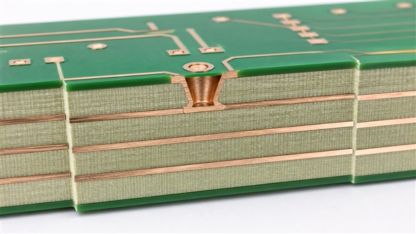
| Hole-wall void | Drilling, desmear, or plating | Hole preparation, bath condition, and current distribution | Microsection and specified tests |
| Solder bridge or insufficient solder | Printing, placement, or reflow | Stencil, paste transfer, alignment, and thermal profile | SPI, AOI, and X-ray when applicable |
| Wrong or reversed component | Kitting or placement | Part identity, feeder setup, and polarity controls | First-piece inspection, AOI, and functional test |
Use this map to start an investigation, not to declare a cause. Confirm the suspected mechanism with physical evidence and process records, contain the traceable exposure, change the responsible control, and monitor equivalent production before closing the action.
Which Manufacturing Requirements Should Be Agreed Before Production?
Production should begin only after the design authority and manufacturer agree on the released data, construction, tolerances, acceptance basis, and verification plan. The manufacturer can identify conflicts and capability risks, but it should not unilaterally select a product class, reinterpret a controlled requirement, or approve its own deviation.
- Released data: Identify the approved fabrication data, drill files, netlist, drawings, BOM, centroid data, and revision.
- Construction: Confirm stackup, materials, copper weights, via structures, finished thickness, impedance needs, finish, solder mask, and legend.
- Critical limits: Mark dimensions, hole sizes, conductor geometry, registration, annular rings, bow and twist, and fit-critical tolerances.
- Acceptance basis: Name the contractually applicable documents, revisions, product classification, customer criteria, deviations, and conflict order.
- Evidence: Define electrical testing, coupons, microsections, impedance reporting, inspection records, assembly tests, and release documentation.
A note such as “build to IPC” is incomplete unless the contract identifies the applicable document and revision. For example, printed-board acceptability, rigid-board performance, soldered assembly process requirements, and assembly acceptability serve different purposes. Confirm which requirements apply instead of treating the documents as interchangeable.
How Do DFM and Data Checks Prevent PCB Fabrication Defects?
DFM prevents defects by resolving geometry, tolerance, and file conflicts before tooling converts them into repeatable production errors. Compare the actual construction with the selected manufacturer’s documented capability; a generic design-rule check cannot account for every registration, plating, material, and assembly interaction.
- Verify identity: Match filenames, revisions, drawing notes, BOM data, netlist, and released outputs.
- Check connectivity: Compare the supplied or independently generated netlist with the intended copper data.
- Review manufacturability: Evaluate conductor spacing, annular rings, hole relationships, aspect ratio, mask clearances, copper balance, routing, and panel constraints.
- Resolve conflicts: Stop tooling when drawings, stackups, drill data, BOM fields, or polarity information disagree.
- Preserve decisions: Link engineering queries, customer responses, tooling changes, and approved deviations to the released revision.
A useful DFM finding identifies the location, manufacturing mechanism, consequence, proposed correction, and approval owner. That information distinguishes a mandatory data conflict from an optional yield improvement.
How Should Incoming Materials and Components Be Verified?
Incoming verification should confirm identity, condition, traceability, storage status, and suitability before material enters production. A certificate supports this review but does not replace comparison of the received lot with the purchase specification and product controls.
- Laminate and copper: Verify manufacturer, grade, thickness, copper weight, lot, shelf life, packaging, and required documents.
- Components: Match manufacturer part number, value, package, polarity, quantity, lot information, and approved-source status to the controlled BOM.
- Moisture-sensitive devices: Check packaging integrity, humidity indication, exposure time, storage, and required handling before placement.
- Process materials: Control chemistry and solder-material identity, condition, expiration, replenishment, contamination, and changeover.
- Changes: Quarantine substitutions and supplier or material changes until technical review and required approval are complete.
Set verification depth by risk. A commercial description can remain unchanged while thermal behavior, drilling response, resin flow, solderability, or long-term performance changes. Base disposition on the product requirement and validation evidence, not the catalog category alone.
How Can PCB Manufacturing Defects Be Reduced Across Imaging, Etching, Drilling, and Plating?
Bare-board defects fall when each fabrication stage has controlled inputs, validated limits, a reaction plan, and verification matched to its failure mechanism. Establish windows for the actual material, geometry, equipment, chemistry, panel loading, and board construction instead of copying universal settings.
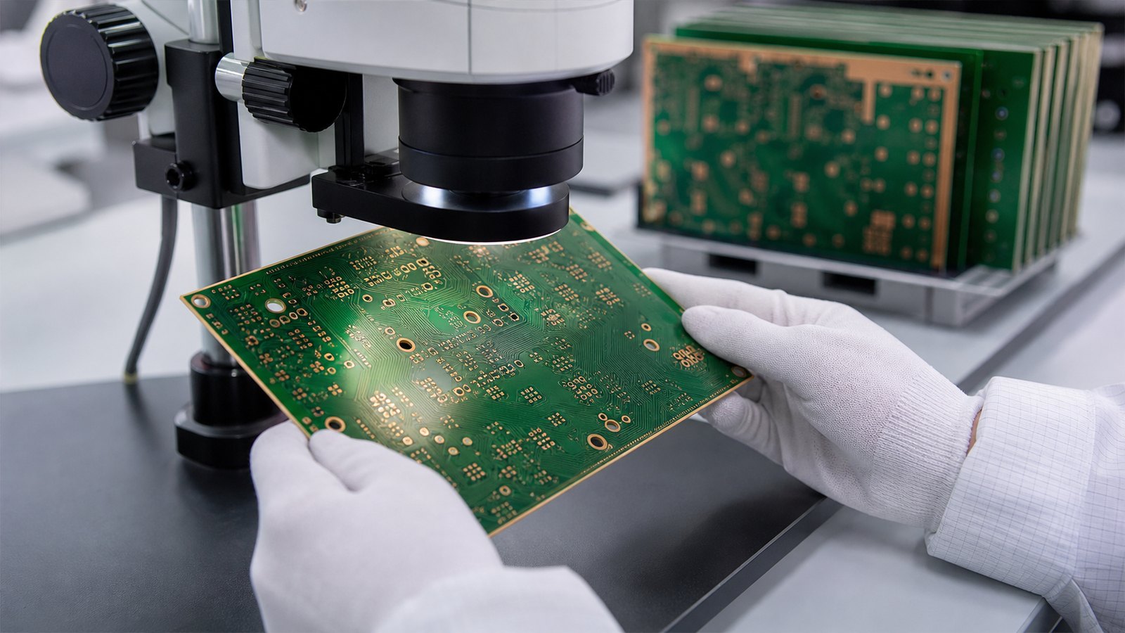
- Imaging: Control artwork, registration, exposure, development, cleanliness, and first-panel verification.
- Etching: Track the conditions that govern rate and uniformity, then measure conductor geometry at representative panel locations.
- Drilling: Control tool selection, stack height, entry and backup materials, feed, speed, hit count, debris removal, and position.
- Hole preparation: Remove resin residue without damaging glass, copper interfaces, or finished hole geometry.
- Plating: Monitor bath condition, current distribution, agitation, electrical contact, loading, and deposits in risk locations.
Sample dense patterns, small holes, high aspect ratios, mixed feature sizes, and uneven copper distributions because they may respond differently within one panel. Agree microsection locations and acceptance criteria before production when structural evidence is required.
How Can Solder Paste, Placement, and Reflow Defects Be Reduced?
Assembly defects decline when printing, placement, and reflow are controlled as one connected process. Paste deposits affect seating, placement affects paste displacement, and the thermal profile controls wetting and joint formation. A change at one stage can move a defect to another instead of eliminating it.
- Stabilize printing: Control stencil identity, apertures, support, paste condition, alignment, separation, cleaning, and deposit verification.
- Protect component identity: Verify feeders, package data, polarity, nozzles, pickup condition, and first-piece placement.
- Control handling: Prevent contamination, excessive flexure, damaged fiducials, mixed revisions, and unmanaged moisture exposure.
- Profile the assembly: Measure the selected paste, board thermal mass, component mix, oven, and loading pattern under actual conditions.
- Correlate evidence: Compare bridges, opens, tombstoning, skew, voiding, and insufficient joints with paste, placement, profile, and material records.
Do not copy a profile from another product without confirming current cold and hot joints. Increasing paste to correct an open can create bridging elsewhere. Trial controlled changes, obtain approval when required, and retain product-specific evidence.
Which Inspection Methods Match Different PCB Defects?
No inspection method detects every defect. Build coverage from the failure mechanism, feature visibility, required sensitivity, and consequence of escape. Inspect close to the creating process so feedback limits suspect quantity and preserves diagnostic evidence.

| Method | Useful Coverage | Decision Boundary |
| Visual inspection | Accessible workmanship, damage, markings, and contamination | Visibility, criteria, lighting, magnification, and consistency limit results |
| AOI | Patterns, placement, polarity, and visible solder conditions | Hidden interfaces and some 3D conditions require another method |
| SPI | Paste area, height, volume, position, and print trends | Acceptable deposits do not prove final joint quality |
| X-ray | Hidden joints, internal features, bridges, void patterns, and alignment | Overlap, resolution, interpretation, and criteria affect detection |
| Microsection | Destructive structural evidence at a selected location | Sampling and preparation determine representativeness |
Challenge inspection programs with known conditions or validated references where practical. Classify false calls rather than allowing routine overrides. Program changes should reduce nuisance alarms without reducing sensitivity to the defects the control is intended to detect.
What Can Electrical and Functional Testing Prove, and What Can They Not Prove?
Electrical and functional tests prove only the connectivity or behavior exercised under the stated test conditions. They do not independently prove workmanship, service life, thermal margin, environmental durability, or the absence of every latent defect.
For bare boards, PCB flying-probe testing or fixture testing can check specified opens and shorts using the approved data and method. Functional assembly testing powers or stimulates selected circuits, but its coverage still depends on access, firmware, loads, timing, measurement limits, and included failure modes.
Build a coverage matrix that links each critical requirement or credible failure mode to prevention, inspection, electrical test, functional test, or external validation. An uncovered row is residual risk; duplicated tests should remain only when they add independent detection value.
How Should Defect Data Drive Containment and Corrective Action?
Defect data should trigger action according to severity, recurrence, escape risk, and process evidence. First identify and hold the affected scope, stop further exposure when necessary, preserve physical evidence, and prevent suspect material from advancing.
- Describe the condition: Record product, revision, lot, location, quantity, process stage, detection method, and acceptance criterion.
- Bound exposure: Use traceability and timing to identify affected incoming material, work in process, finished goods, and shipments.
- Separate occurrence and escape: Determine why the defect formed and why existing controls failed to contain it.
- Verify the mechanism: Test the suspected cause against physical evidence and process records.
- Correct the system: Change the responsible design rule, material control, process, maintenance, instruction, program, fixture, training, or supplier control.
- Confirm effectiveness: Monitor an agreed production quantity or period and verify that both formation and escape remain controlled.
Yield and Pareto charts support decisions only when definitions are stable and severe low-frequency defects are not hidden by aggregate results. Where traceability permits, review trends by product, revision, mechanism, location, machine, material lot, shift, and time.
What Quality Evidence Should You Request From a PCB Manufacturer?
Request evidence connecting your board’s risks to the manufacturer’s proposed controls. A certificate, equipment list, or capability statement supports screening but does not prove that the construction was reviewed, required tests were quoted, or deviations will be controlled.
- DFM records: Confirm how conflicts, exceptions, stackup decisions, and proposed changes are documented and approved.
- Control evidence: Identify critical inputs and outputs, monitoring methods, limits, and reactions for the proposed construction.
- Inspection and testing: Request methods, coverage or sampling basis, criteria, report format, and handling of failures and retests.
- Traceability: Determine how materials, batches, revisions, process records, test results, and deviations remain connected.
- Change management: Define which material, supplier, equipment, process, tooling, software, or location changes require review.
- Corrective action: Confirm how escapes are contained, evidence is preserved, causes are verified, and effectiveness is checked.
Published PCB manufacturing capabilities can support early screening. The RFQ still needs controlled data, construction, quantities, application risks, acceptance requirements, testing, documentation, and revision status.
Which PCB Defect-Prevention Questions Come Up Most Often?
Q1: Does a higher IPC product class automatically reduce PCB defects?
A1: No. Product class does not stabilize design data or production by itself. The design or contractual authority selects it, and the manufacturer must support it with appropriate design rules, materials, controls, inspection, and testing.
Q2: Does prototype approval guarantee stable production yield?
A2: No. Prototype approval does not represent every volume-production condition. Scale-up changes material lots, panel loading, utilization, tooling wear, and opportunities for variation. Freeze the release and define first-article, process, test, and change controls before volume production.
Q3: What should happen when customer files conflict?
A3: Pause production until an authorized party resolves the conflict. Record the affected files, revisions, locations, consequences, response, and corrected release. Tooling should not silently choose between inconsistent inputs.
Q4: Can a reworked PCB meet the original acceptance requirements?
A4: It can when the contract permits the method and the finished result is reverified. Evaluate additional risks such as heat exposure, pad damage, contamination, conductor repair, and repeated handling.
Q5: Can a golden sample replace controlled drawings and production data?
A5: No. A sample cannot define hidden layers, connectivity, tolerances, materials, test limits, or revision history. Use it only for an approved purpose such as appearance, orientation, mechanical fit, or workmanship reference.
Q6: Should every PCB defect use the same sampling plan?
A6: No. Sampling must reflect severity, detection capability, and escape risk. Critical electrical characteristics may require 100% testing, while destructive checks need a representative plan tied to construction and contractual requirements.
Q7: When does a manufacturing deviation need customer approval?
A7: Approval is required whenever the controlled requirement reserves disposition for the customer. Record the exact condition, quantity, risk, proposed disposition, and traceable authorization before release.
Q8: Which records should be preserved for repeat PCB orders?
A8: Preserve the controlled release and every approved decision that changed it. Link stackup, tooling, materials, process records, tests, deviations, dispositions, and corrective actions to the repeat-order revision.
Q9: When should a process change trigger requalification or new validation?
A9: Review a change before release whenever it can affect a qualified or validated condition. Select evidence according to the risk created by changes in materials, suppliers, equipment, software, tooling, location, panelization, soldering, or testing.
Q10: Can final inspection compensate for an unstable manufacturing process?
A10: No. Final inspection cannot detect every hidden, intermittent, latent, or marginal condition. Tighten containment when needed, but correct the upstream source instead of relying on additional sorting.
Conclusion
Defect reduction depends on controlling the path from released data to corrective-action evidence. Agree requirements, perform construction-specific DFM, verify incoming materials, maintain measurable fabrication and assembly windows, and match each inspection or test to a credible failure mechanism.
Compare suppliers by the evidence they can provide for your board rather than broad quality claims. A complete RFQ and disciplined application of best practices for reducing PCB defects in manufacturing make technical review, production release, and repeat orders easier to control.
You may also like




Tags: PCB defects, pcb manufacturing, PCB Quality Control, PCB testing