PCB manufacturing PCB manufacturing
Home > Blog

pcb failure analysis

PCB Pink Ring Defect: Causes, Inspection, and Prevention
Saturday, September 5th, 2026
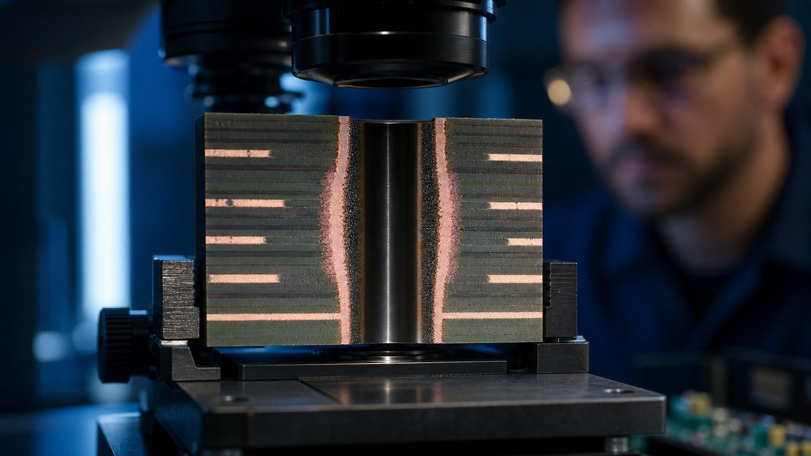
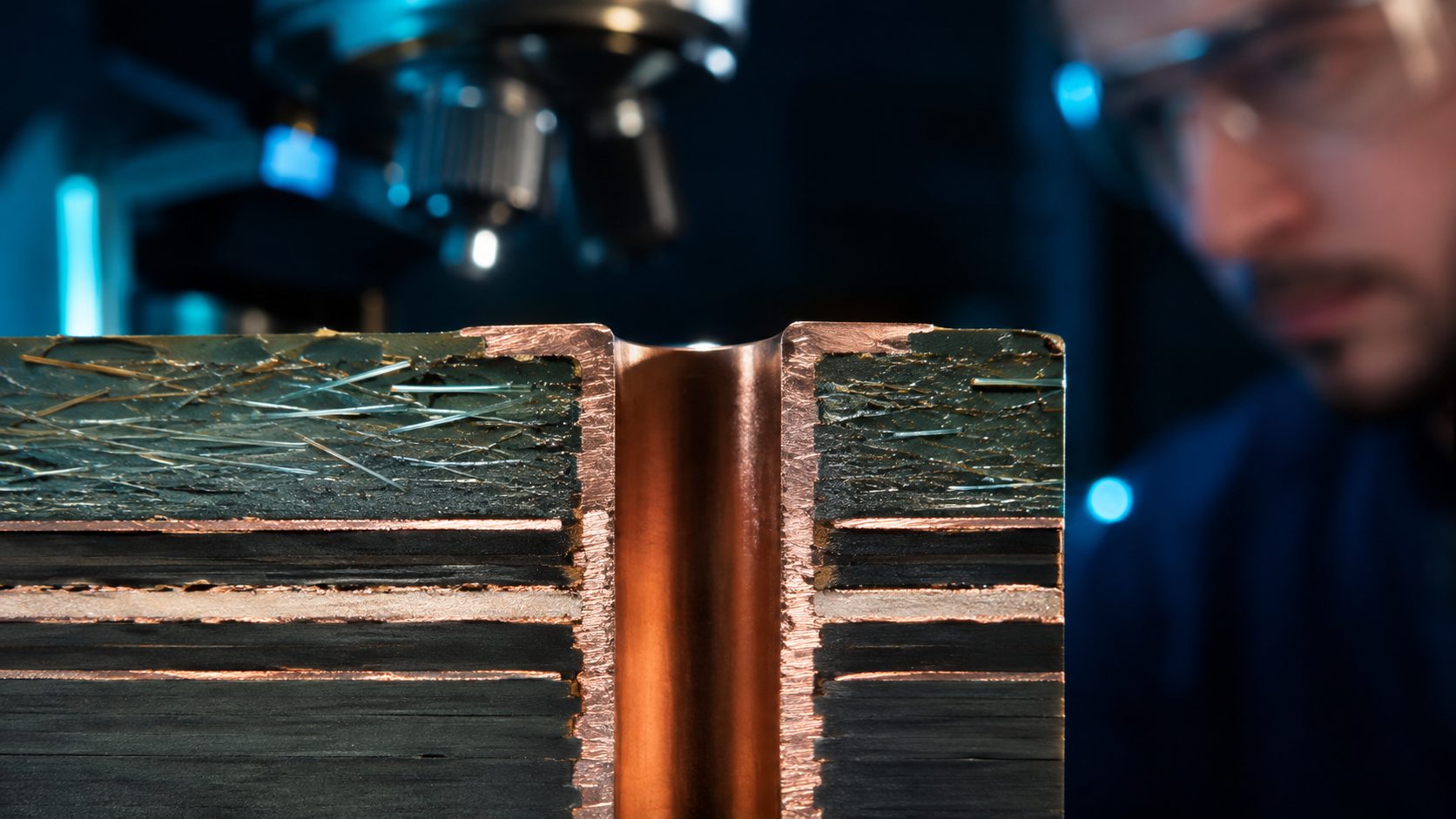
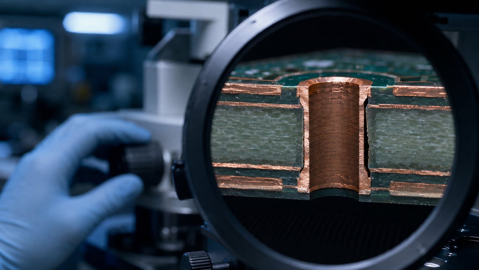
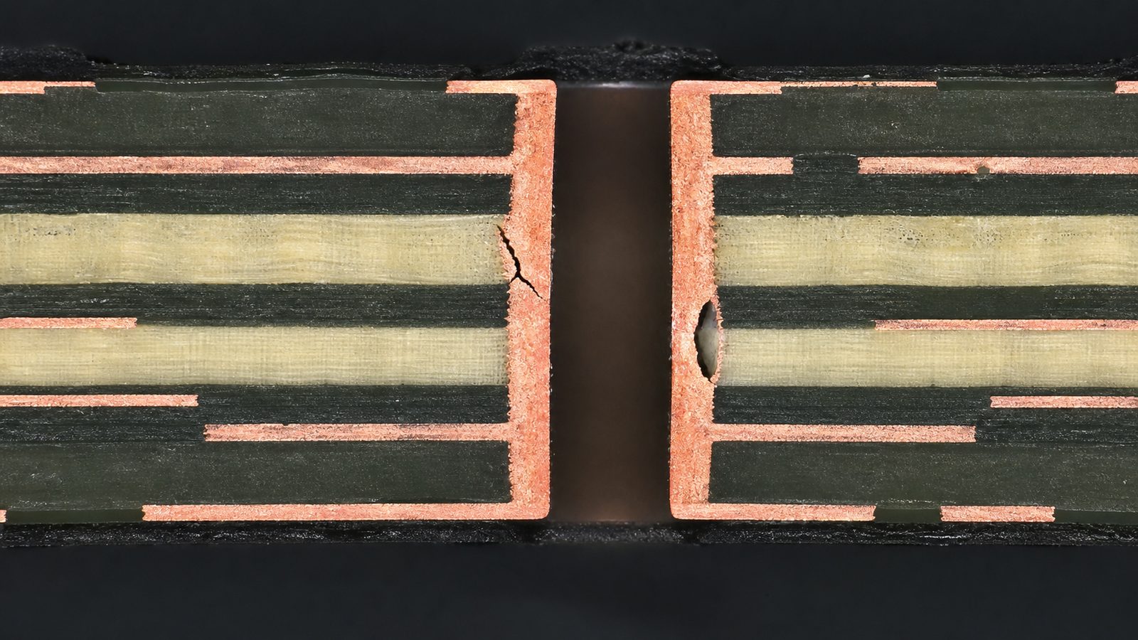
Multilayer PCB microsection showing a pink copper-colored ring around a plated through-hole
A PCB pink ring is a multilayer-interface observation around a drilled hole, not a pink solder-mask color choice.

The PCB pink ring defect is a pink or copper-colored halo around a drilled hole where the dark inner-layer bond-treatment appearance has been removed or recessed. It is normally evaluated in a multilayer PCB cross-section or after destructive inspection. The color change alone does not prove electrical failure, but it signals that engineers should examine the copper-to-resin bond interface, process history and applicable acceptance criteria.

Do not confuse this condition with annular-ring breakout, a pink solder mask, measling or a plating void. Those findings occur in different materials and require different corrective actions. A useful investigation records the ring extent, affected layers, hole types, panel locations and whether associated separation is present.

What the PCB Pink Ring Defect Actually Is

Pink ring describes the visible exposure of copper-colored inner-layer material around a hole after part of a dark oxide or oxide-alternative surface treatment is lost or attacked. The feature is associated with the treated copper/resin interface in multilayer construction. It can appear as a narrow circumferential band or as an uneven local halo.

The observation should be separated from its root cause. The ring can be influenced by bond-treatment condition, lamination, drilling, hole-wall cleaning and chemical exposure. Its presence does not identify which process created it, and an apparently uniform ring does not show whether the remaining bond is adequate.

A report should state whether the feature was found in an as-produced coupon, a production board, a thermally stressed specimen or a section prepared after field failure. That context changes how the image is interpreted.

Why the Ring Looks Pink Around a Plated Hole

The exposed underlying copper looks pink compared with the darker treated copper surface surrounding it. The contrast makes the condition visually obvious even when the actual affected distance is small. Lighting, etching and camera settings can change the apparent color, so measure geometry rather than judging severity from saturation.

The halo follows the hole because drilling and subsequent hole preparation act at that boundary. If chemistry penetrates along the treated interface or if the bond-treatment layer is locally removed, the copper color becomes visible around the circumference.

Document the ring at each affected internal layer. A single top-view photograph cannot show whether the feature is limited to one interface or repeats through the stackup.

Pink Ring vs Annular-Ring Breakout, Measling, and Solder-Mask Color

Finding Where it appears Key distinction Review focus
Pink ring Inner-layer treated-copper interface around a hole Pink/copper halo replaces darker bond-treatment appearance Bond interface and multilayer process history
Annular-ring breakout Copper land around the drilled hole Hole position removes part of the designed land Registration, drill size and pad geometry
Measling/crazing Glass-resin laminate White or cloudy fiber-related marks Laminate stress, moisture and handling
Pink solder mask External board coating Intentional overall or patterned mask color Artwork and mask specification
Plating void Deposited copper barrel Missing/discontinuous copper rather than a surface-treatment halo Activation, deposition and plating

For white laminate marks, use the dedicated guides to PCB measling and PCB crazing. Combining these labels into “laminate damage” hides the process evidence needed for a useful response.

How Oxide and Oxide-Alternative Bond Treatments Affect the Interface

Inner-layer bond treatment prepares copper so the surrounding resin can develop a controlled interface during lamination. Traditional oxide and oxide-alternative processes use different surface chemistries and textures, but both must remain compatible with the material system and later processing.

Investigate treatment concentration, temperature, dwell, rinsing, loading, contamination and hold time before layup. Also check whether the treated panels were handled, stored or exposed outside the controlled route. A chemistry reading inside its nominal range does not prove every panel received uniform treatment.

Lamination completes the interface. Review prepreg selection, resin flow, vacuum, pressure, temperature and cure records together with the bond-treatment data. Do not change chemical settings before checking whether the feature follows a press load, panel position or material lot.

Why Drilling and Hole Preparation Can Expose the Condition

Drilling opens the multilayer interface, while desmear and conditioning expose the hole wall to mechanical and chemical action. The combination can reveal or enlarge a susceptible treated-copper boundary.

  • Review drill diameter, tool type, hit count, feed and spindle settings.
  • Check entry/backer materials, panel stack height and heat generation.
  • Inspect hole-wall roughness, smear and glass-fiber condition separately.
  • Review desmear chemistry, dwell, loading, agitation and rinse control.
  • Compare small and large holes and different panel positions.
  • Map affected layers against copper density and stackup construction.
  • Check metallization and plating for separate void or barrel concerns.

More aggressive desmear is not a universal fix. It may remove residue but can also increase attack at a vulnerable interface. Use controlled trials tied to the confirmed mechanism.

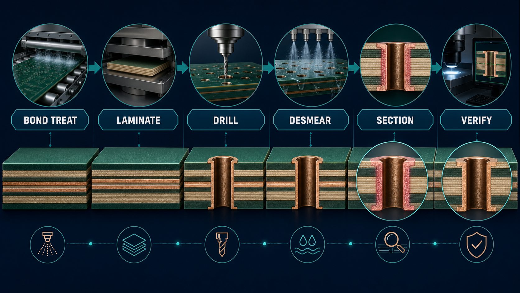
PCB pink ring prevention workflow covering bond treatment, lamination, drilling, desmear, sectioning and verification
Pink-ring prevention depends on a controlled process chain and a verified section, not one isolated setting.

What Pink Ring Does and Does Not Prove About Reliability

Pink ring proves that the interface appearance changed; it does not by itself prove delamination, an open circuit or future field failure. Reliability significance depends on the remaining bond, associated separation, ring extent, product requirement, environment and evidence from representative samples.

Look for related conditions such as inner-layer separation, resin recession, barrel cracks, plating voids or laminate damage. If none is present, the disposition may differ from a section showing a visible gap or failed interconnect. Use the governing customer and product specification rather than a threshold copied from an unrelated source.

Electrical test cannot characterize the bond interface. A board may pass continuity while a structural concern remains. Conversely, a pink appearance does not establish an electrical defect without supporting evidence.

Need an evidence-based review of a pink-ring finding?

Send the full microsection images, stackup, material callout, bond-treatment route, drill data, desmear history and lot map. EBest Circuit can identify missing evidence before a disposition or corrective rebuild.

Inspection Evidence Needed Before Lot Disposition

A defensible report connects each image to a board, lot, location and preparation condition. Include:

  • part number, revision, production lot and panel position;
  • stackup, affected layer and hole type;
  • full-hole overview plus detailed images with scale;
  • section orientation and confirmation that the cut is centered;
  • ring extent around the circumference and at each layer;
  • sample count and number of affected holes;
  • associated separation, void, crack or laminate observations;
  • thermal conditioning and sample-preparation history;
  • comparison with a known-good or unaffected location;
  • acceptance reference and named disposition authority.

The PCB microsection analysis guide provides a broader framework for preparing sections and turning images into an actionable report.

A Root-Cause Sequence for Pink Ring Findings

  1. Confirm: repeat questionable sections and rule out polishing or etching artifacts.
  2. Map: record affected layers, hole sizes, panel positions and frequency.
  3. Contain: preserve lots and unused samples while risk is evaluated.
  4. Correlate: compare treatment, layup, press, drill and desmear batches.
  5. Separate: identify any associated delamination, voids or interconnect defects.
  6. Hypothesize: rank causes that match both morphology and process pattern.
  7. Trial: change one controlled contributor where practical.
  8. Verify: rebuild and inspect representative coupons/boards using the agreed sequence.

If the feature clusters by one treated-inner-layer batch, investigate upstream. If it follows a drill tool or hole size, examine mechanical preparation. If it follows one desmear load or panel position, chemistry uniformity becomes more likely. Correlation guides the trial; it does not replace verification.

Containment While the Cause Is Still Open

Containment should prevent uncontrolled shipment and preserve the evidence needed for the permanent fix.

  • Define suspect lot boundaries and downstream locations.
  • Segregate suspect, screened, accepted and rebuilt material.
  • Maintain panel, material, treatment, press, drill and chemistry traceability.
  • Reserve unsectioned samples from affected and comparison groups.
  • Document any temporary screen and its detection limits.
  • Prevent extra thermal or chemical exposure from changing the evidence.
  • Set the responsible disposition authority and next review point.

Do not call screening a corrective action. A screen may remove visible extremes while leaving the cause unchanged.

Cause-Specific Corrective Actions and Verification

Confirmed pattern Corrective direction Verification evidence
Bond-treatment batch correlation Restore chemistry, rinsing, loading and hold-time controls Controlled treated-panel comparison and sections
Lamination/load correlation Correct material, layup, vacuum or press-cycle control Actual press chart plus mapped rebuild sections
Drill-tool/hole-size correlation Adjust tool life, parameters or stack conditions Controlled drill trial through plating and section
Desmear-load correlation Correct bath control, exposure and uniformity Chemistry records plus representative hole sections
Preparation artifact Correct mounting, polishing or etching Independent repeat sections without the false feature

Verification should reproduce the relevant construction and process route. One clean microsection from an unrepresentative coupon is weaker than a mapped sample across the corrected build.

PCB Data and Records to Send for Engineering Review

  • Gerber or ODB++, controlled fabrication drawing and revision;
  • stackup, laminate/prepreg and copper-weight callouts;
  • NC drill files and drill table;
  • acceptance class or customer-specific requirement;
  • full-resolution micrographs with sample identification;
  • lot/panel map and observed frequency;
  • bond-treatment, lamination, drilling and desmear records;
  • thermal, assembly or rework history;
  • current containment status and response deadline;
  • quantity and target delivery if a corrective build is required.

Turn the finding into a controlled PCB build plan

Include design data, material/stackup, hole information, acceptance requirement and the original inspection package so manufacturing and verification requirements can be reviewed together.

FAQ About PCB Pink Ring

Is PCB pink ring the same as a pink circuit board?

No. Pink ring is a local multilayer-interface condition around a drilled hole. A pink PCB normally refers to an intentional solder-mask color.

Does pink ring mean the annular ring is too small?

No. Annular-ring breakout concerns pad geometry and registration. Pink ring concerns the treated inner-layer copper/resin interface.

Can pink ring be seen from the board surface?

It may be suspected during destructive inspection, but a prepared cross-section is normally needed to understand affected layers and associated conditions.

Is every pink ring rejectable?

No universal disposition applies. Use the governing requirement, measured extent, associated defects, representative sampling and product risk.

Does pink ring always cause electrical failure?

No. The color change alone does not establish an open or short. It must be evaluated as part of the structural and process evidence.

Can desmear cause pink ring?

Hole-preparation chemistry can contribute, but bond treatment, lamination, drilling and material conditions must also be correlated before assigning cause.

Can microsection preparation create a misleading ring?

Yes. Polishing and etching can change contrast or produce artifacts, so questionable findings should be repeated with controlled preparation.

What should be measured?

Record affected layers, circumferential extent, radial distance, frequency and any associated gap, void or laminate damage using the agreed method.

What records are most useful?

Bond-treatment, press, material, drill and desmear traceability are especially useful when paired with a panel map and full micrographs.

How is prevention verified?

Use a controlled build with the confirmed correction, then repeat the agreed sectioning and sampling plan across representative locations.

Final Prevention Checklist

  • Define pink ring separately from breakout, measling and plating defects.
  • Control inner-layer treatment, handling and time to lamination.
  • Verify material, layup and actual press-cycle records.
  • Control drill tool life and hole-preparation chemistry.
  • Map findings by layer, hole, panel and lot.
  • Use representative microsections and an agreed acceptance basis.
  • Link the correction to confirmed cause evidence.
  • Verify a controlled rebuild before closing the action.

Request a multilayer PCB engineering and quotation review.

Send Gerber or ODB++, stackup, drill files, material callout, micrographs, process history, quantity and target delivery to sales@bestpcbs.com, or use the PCB quote form. EBest Circuit will identify missing evidence and align fabrication and inspection requirements before production.

You may also like

PCB Resin Recession: Identification, Causes, and Prevention
Saturday, September 5th, 2026
PCB microsection showing resin recessed beside a plated through-hole barrel
Resin recession is interpreted from the resin, glass and copper geometry in a controlled PCB cross-section.

PCB resin recession is a cross-sectional condition in which resin has receded from its expected boundary around a drilled or plated feature, leaving glass bundles or adjacent structures comparatively exposed. It is not automatically the same as copper-to-hole-wall pullaway, resin smear or a lamination void.

The practical question is not simply whether one dark or recessed area appears in a micrograph. Engineers must confirm the morphology, preparation quality, extent, test history and applicable acceptance criteria before assigning a root cause or lot disposition. A defensible investigation separates observation from interpretation and interpretation from corrective action.

What PCB Resin Recession Looks Like

In a prepared microsection, resin recession appears as resin pulled back or missing relative to nearby glass reinforcement, copper or the intended laminate boundary. The feature may be local around a hole wall or visible near internal-layer edges. Its shape and position should be documented across the entire section, not inferred from a tightly cropped image.

Look for exposed glass ends, a recessed resin boundary and whether the copper barrel remains intact and supported. Record the layer, quadrant, depth and length of the indication. Compare more than one hole and, when possible, compare suspect material with a known-good construction prepared by the same method.

Polishing relief can imitate recession. Soft resin and hard glass or copper remove at different rates during specimen preparation. If the indication changes substantially with preparation technique or appears only at a poorly supported edge, repeat the section before treating it as a production defect.

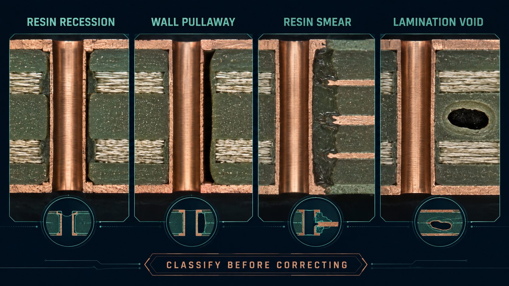
Resin Recession vs Hole Wall Pullaway, Smear, Starvation, and Voids

Classify the material or interface that is missing, displaced or separated before selecting corrective action.

Finding Defining location Key visual clue Investigation focus
Resin recession Resin boundary near glass/copper Resin sits back while reinforcement or adjacent geometry is exposed Material, lamination, thermal history and preparation artifact
Hole wall pullaway Copper-barrel-to-dielectric interface Gap follows the interface beside an otherwise recognizable barrel Interface preparation and interconnect reliability
Resin smear Drilled wall or inner-layer connection Resin coats or obscures copper that should be exposed Drilling heat and desmear effectiveness
Resin starvation Broader laminate region Insufficient resin wet-out around reinforcement Prepreg selection, layup and resin flow
Lamination void Inside the dielectric Enclosed cavity rather than a recessed surface boundary Layup, vacuum, pressure and entrapped volatiles
Comparison of PCB resin recession, hole wall pullaway, resin smear and lamination void morphologies
Similar-looking cross-section findings can point to different process checks; classify before correcting.

For a focused explanation of copper-interface separation, use our PCB hole wall pullaway guide. The distinction matters because increasing desmear, changing a press cycle or altering a plating process are not interchangeable remedies.

Why Recession Can Become More Visible After Thermal Stress

Thermal exposure can change the apparent or actual geometry because resin, glass and copper respond differently to heat, moisture and repeated expansion. This does not mean thermal stress is always the original cause. It may reveal a pre-existing material or process weakness, exaggerate a preparation-related feature, or create a condition beyond the product’s normal use.
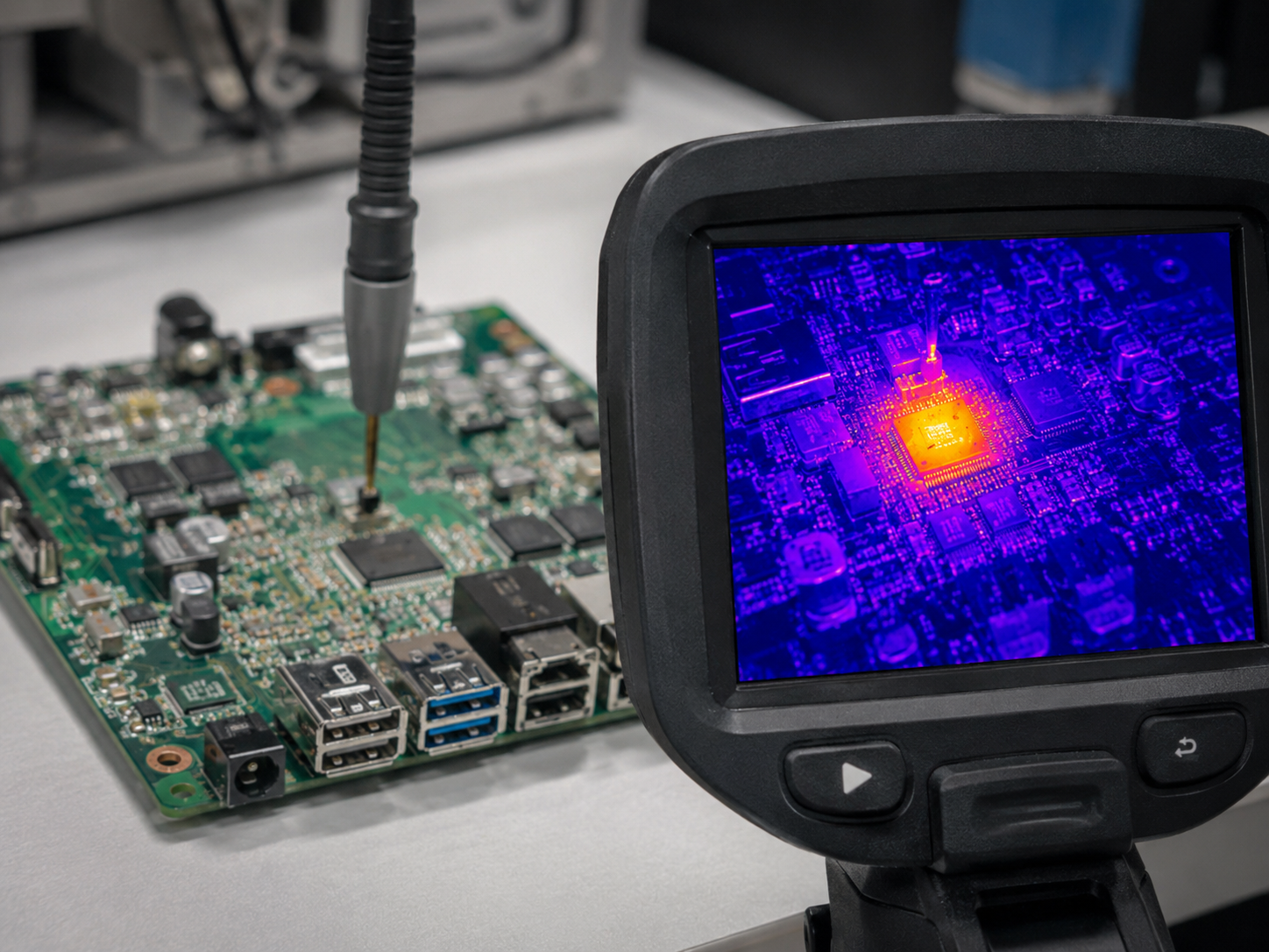
Always identify whether the section was examined as received, after baking, after solder float, after reflow simulation, or after another conditioning sequence. Record temperature, dwell, cycles, ramp, cooling and moisture conditioning. Without that information, a before/after comparison cannot be reproduced.

When the concern appeared after assembly, include the actual reflow and rework history. Multiple local rework cycles may produce a different exposure from one qualified production profile. Our solder float test guide explains why the specified test method and post-stress evidence must travel together.

A Microsection Sequence That Preserves Evidence

A controlled sequence should produce comparable sections without consuming every suspect sample.

  1. Identify part, revision, lot, panel position, hole type and downstream history.
  2. Reserve untested specimens and known-good comparison material.
  3. Photograph the board and mark the intended section plane.
  4. Mount and support the specimen so the hole remains centered and edges are protected.
  5. Grind and polish progressively, avoiding excessive heat or pressure.
  6. Capture a full-hole overview before higher-magnification details.
  7. Record resin, glass, barrel and inner-layer geometry separately.
  8. Apply any agreed thermal stress to a separate or documented specimen group.
  9. Compare frequency and extent across locations, lots and conditions.
  10. Retain images, raw measurements, unused samples and the preparation record.

A single attractive micrograph is not a sampling plan. For broader specimen and report requirements, see how PCB microsection analysis finds hidden defects.

Unsure whether the section shows recession or another defect?

Send the original overview and detail micrographs, stackup, material callout, drill data, sample condition and thermal history. EBest Circuit can identify what additional evidence is needed before a process change or rebuild.

Material and Lamination Conditions to Investigate

Resin recession can reflect the material system, its condition and the way the multilayer was laminated, but no one factor should be declared causal without correlation.

Area Question Evidence
Material construction Is the prepreg/resin system appropriate for the stackup and thermal exposure? Controlled stackup, material designation and supplier lot
Storage and handling Could moisture or out-of-control storage affect behavior? Receiving, storage, floor-life and bake records
Layup Is resin distribution consistent around dense copper and drilled regions? Artwork, copper balance, prepreg selection and panel map
Press cycle Did temperature, pressure, vacuum and cure remain within the controlled recipe? Actual press chart and lot traveler
Thermal history Was the construction exposed beyond the qualified sequence? Fabrication, assembly, rework and test profiles

Compare the finding with resin-rich and resin-poor areas, different panel locations and more than one material lot. If the feature follows copper density rather than the drill tool, lamination and local resin-flow evidence deserve closer attention.

Drilling and Hole Preparation Checks

Drilling and desmear determine the surface that later receives metallization, so their records help distinguish true recession from smear, roughness or preparation damage.

  • Review drill diameter, tool type, hit count and actual tool-change interval.
  • Check feeds, spindle speed, entry/backer materials and panel stack height.
  • Inspect unplated hole walls when retained process coupons are available.
  • Compare high-copper and low-copper panel regions.
  • Review desmear chemistry, concentration, temperature, dwell, loading and agitation.
  • Confirm conditioning and metallization followed the controlled process window.
  • Look for smear, glass-fiber protrusion, gouging, voids and barrel discontinuity as separate findings.

Do not respond to suspected recession by simply increasing chemical attack. An aggressive change may alter the hole wall in another way. Trial the cause-specific adjustment and compare controlled sections.

How to Read Extent, Location, and Frequency

The decision value of a finding comes from its distribution, not only its maximum-looking example. Record how many inspected holes show the condition, where it appears around each circumference, its approximate extent and whether it clusters by layer, panel region, hole size or thermal condition.

A repeated feature at the same depth can point toward construction or process interaction. A feature concentrated near one panel edge may justify reviewing press or chemistry uniformity. A correlation with one drill tool suggests a different path. No correlation is also evidence: it means the investigation should remain open rather than forcing the first explanation.

Use measurement methods agreed by the customer, supplier and applicable specification. Avoid extracting a universal acceptance limit from an unrelated image or article; product class and customer requirements control the final disposition.

Containment Before Root Cause Is Confirmed

Containment protects product and evidence while the investigation is still uncertain.

  1. Identify the suspect lot boundaries and all downstream locations.
  2. Segregate suspect, screened, accepted and rebuilt material.
  3. Preserve traceability to panels, materials, drill tools and press/plating batches.
  4. Reserve representative samples before destructive analysis.
  5. Define any temporary screen and document what it cannot detect.
  6. Stop uncontrolled extra thermal exposure that could change the evidence.
  7. Assign disposition authority and a deadline for the next evidence review.

Containment does not prove acceptability. If product has already entered assembly or the field, risk evaluation must include application, thermal/mechanical stress and the possibility of associated interconnect defects.

Cause-Specific Corrective Actions and Verification

A corrective action is credible only when it follows confirmed evidence and passes a controlled verification.

Evidence pattern Action direction Verification
Material or storage-lot correlation Correct material control, conditioning or approved construction Traceable comparison build and repeat sections
Press-cycle or panel-position correlation Restore recipe, vacuum, pressure or loading uniformity Actual press chart plus mapped microsections
Drill-tool correlation Adjust tool-life/parameter control Controlled drill trial before and after plating
Preparation artifact Correct mounting, grinding and polishing method Independent repeat sections
Excess downstream thermal exposure Control assembly/rework profile Qualified profile followed by agreed inspection

Changing material, drilling, desmear and lamination simultaneously can hide the true contributor. When practical, isolate variables and retain the evidence that proves the improved outcome is repeatable.

What to Send for Supplier Engineering Review

A review can move faster when design data, specimen identity and process history arrive together.

  • Gerber or ODB++, fabrication drawing and controlled revision;
  • stackup, material designation and prepreg construction;
  • NC drill files, drill table and relevant hole structures;
  • product class, customer specification and acceptance question;
  • lot, panel and sample traceability;
  • full-resolution overview/detail micrographs;
  • sample preparation method and operator/lab identity;
  • thermal conditioning, soldering and rework profiles;
  • quantity affected, containment status and required response date;
  • target build quantity and delivery requirement if a rebuild is requested.

Prepare a controlled PCB review or rebuild package

Include the design files, material/stackup, drill data, acceptance requirement, original images and thermal history. We will separate the immediate containment question from DFM, inspection and production requirements.

FAQ About PCB Resin Recession

Is resin recession always a rejectable PCB defect?

No universal answer applies. The governing product/customer requirement, morphology, extent, sampling, associated defects and end-use risk determine disposition.

Is resin recession the same as hole wall pullaway?

No. Recession describes resin pulled back from its expected boundary. Pullaway describes separation at the copper-barrel-to-dielectric interface. Both can appear near a plated hole.

How is resin recession different from resin smear?

Smear is unwanted resin left on a drilled wall or inner-layer copper. Recession is resin absent or set back relative to surrounding geometry.

Can polishing create apparent resin recession?

Yes. Differential removal of soft resin, glass and copper can produce relief. Repeat preparation and comparison specimens help test that explanation.

Can visual inspection find resin recession?

Usually not from the PCB surface. A controlled cross-section is normally needed to see and interpret the internal geometry.

Does thermal stress cause every case?

No. Thermal exposure may reveal or enlarge a condition, but material, lamination, drilling, preparation and specimen artifacts must also be investigated.

What should a microsection image include?

Include a full-hole overview and detailed views with scale or magnification, sample identity, orientation, preparation condition and thermal history.

How many holes should be inspected?

The sampling plan should reflect the governing requirement, lot risk and observed distribution. One hole cannot normally establish lot-wide frequency.

Can electrical test prove the laminate interface is acceptable?

No. Electrical continuity can pass while a structural finding remains. Use electrical results with microsection, process and reliability evidence.

What proves a corrective action worked?

A traceable controlled build using the confirmed change, followed by the agreed sampling, conditioning and inspection sequence, provides stronger proof than a single passing section.

Final Acceptance and Prevention Checklist

  • Confirm the feature is real and not specimen-preparation relief.
  • Differentiate recession from pullaway, smear, starvation and voids.
  • Define sample count, distribution and thermal condition.
  • Use the correct customer or product acceptance requirement.
  • Preserve lot, panel, material and process traceability.
  • Link root cause to physical and process evidence.
  • Verify the specific correction on a controlled build.
  • Update drawings, inspection plans and supplier records where needed.

Get an evidence-led PCB manufacturing review.

Send Gerber or ODB++, stackup, drill files, material callout, micrographs, lot history, thermal profile, quantity and target delivery to sales@bestpcbs.com, or use the PCB quote form. EBest Circuit will identify missing evidence and align inspection requirements before production or a corrective rebuild.

You may also like

PCB Hole Wall Pullaway: Causes, Inspection, and Prevention
Saturday, September 5th, 2026
Metallurgical microscope inspection of PCB hole wall pullaway in a plated through-hole cross-section
Hole wall pullaway is confirmed from a prepared cross-section, not from a surface photograph alone.

PCB hole wall pullaway is a separation between the plated copper barrel and the surrounding dielectric along a drilled hole. It is a cross-sectional finding, and it should not be diagnosed from a vague electrical failure or a top-view image. The first job is to confirm where the separation exists, whether it appeared before or after thermal stress, and whether other plated-through-hole defects are present.

A confirmed finding does not automatically prove one root cause or justify scrapping every board. Quality teams need representative samples, controlled microsection preparation, lot traceability and a cause-specific corrective-action plan. This guide gives designers, buyers and supplier-quality engineers a practical sequence for making that decision.

What PCB Hole Wall Pullaway Looks Like in Cross-Section

The characteristic feature is a visible gap at the interface between the plated hole copper and the resin/glass wall. The separation may be local or extend along part of the barrel. Its position, length, frequency and relationship to internal-layer connections should be recorded rather than reduced to a simple pass/fail label.

A useful micrograph shows the full hole, the affected interface and enough magnification to distinguish a true gap from polishing relief. The report should identify the board, lot, coupon or production location, section orientation, preparation condition and whether the specimen was thermally stressed.

Preparation artifacts can mimic separation. Excessive grinding pressure, poor specimen support, smeared resin, edge rounding or unsuitable etching can distort the interface. When the feature appears only on one questionable section, prepare another specimen before assigning a manufacturing cause.

Why Hole Wall Pullaway Matters After Thermal Stress

Pullaway matters because the plated barrel and dielectric experience different mechanical and thermal behavior, and loss of support can accompany a broader interconnect-reliability problem. The actual product risk depends on location, extent, associated cracks or voids, copper condition, end-use stress and the governing acceptance requirement.

A feature visible before stress points the investigation toward material condition, hole preparation, lamination and plating history. A feature that appears or grows after a defined thermal exposure may indicate that the interface could not tolerate the applied expansion and contraction. The test method, temperature profile, dwell, cycles and sample conditioning therefore belong in the evidence package.

Do not use one dramatic micrograph to generalize across a production lot. Sampling must cover relevant panel positions, hole sizes, constructions and process batches. Electrical continuity alone also cannot reveal every developing interface problem.

Hole Wall Pullaway vs Plating Voids, Barrel Cracks, and Hole Breakout

Similar-looking hole defects require different corrective actions, so classify the morphology before changing the process.

Finding Where it appears Diagnostic clue Primary review direction
Hole wall pullaway Copper-to-dielectric interface Gap follows part of the hole wall Interface preparation, material and thermal history
Plating void Within or missing from deposited copper Discontinuous copper coverage rather than interface separation Cleaning, activation and deposition/plating control
Barrel crack Across plated copper Fracture passes through the copper wall Copper properties, thickness, geometry and thermal strain
Inner-layer separation Barrel-to-inner-layer junction Connection defect is concentrated at an internal pad Desmear, etchback and interconnect formation
Hole breakout Annular ring at a land Drill position removes part of the surrounding pad Registration, drill size and annular-ring design

A board can contain more than one defect. Record each morphology independently. For broader context on how prepared sections reveal hidden features, see the PCB microsection analysis guide.

A Practical Failure-Analysis Sequence

Contain the lot first, preserve evidence, then test competing explanations in a controlled sequence.

  1. Contain: identify affected lots, panels, date codes and downstream assemblies without destroying evidence.
  2. Document: save failure symptoms, inspection images, test history and the exact acceptance concern.
  3. Sample: select suspect and known-good boards across relevant panel positions and hole structures.
  4. Section: prepare representative holes with controlled orientation and record pre-stress condition.
  5. Stress: apply only an agreed test profile when comparison after thermal exposure is needed.
  6. Inspect: measure and photograph the interface, barrel, inner-layer junctions and nearby laminate.
  7. Correlate: compare findings with material lots, lamination, drilling, desmear and plating records.
  8. Correct and verify: change the confirmed contributor, then validate with a controlled rebuild.
PCB hole wall pullaway failure analysis workflow from containment through verified corrective action
A controlled workflow prevents a single micrograph from becoming an unsupported root-cause conclusion.

Need a second review of a plated-hole finding?

Send the stackup, drill table, material callout, lot history, micrographs and thermal-stress conditions. EBest Circuit can review whether the evidence supports a pullaway diagnosis and what additional data is needed before a rebuild.

Process Conditions That Can Contribute to Pullaway

Hole wall pullaway is usually investigated as an interaction among material condition, lamination, mechanical drilling, hole-wall preparation and later thermal exposure. A list of possible causes is not a root-cause report; each candidate must be matched to records and physical evidence.

Process area Condition to investigate Evidence that helps
Incoming laminate and prepreg Material condition, storage or construction variation Material certificates, lot traceability and controlled comparison
Lamination Resin flow, cure history or local stress around the hole structure Press recipe, stack records and sections from multiple locations
Drilling Smear, roughness, heat damage or tool wear Tool count, hit count, feeds/speeds and unplated-hole inspection
Desmear and conditioning Insufficient, excessive or nonuniform wall preparation Chemistry control, dwell records and hole-wall morphology
Metallization and plating Poor initial coverage or weak interface formation Bath controls, deposition records and copper continuity
Thermal exposure Stress beyond the qualified construction or repeated excursions Assembly/rework profile, test profile and before/after sections

Correlation is essential. If the finding clusters by one drill tool, panel region or material batch, that pattern is more useful than a generic assumption. If it appears across unrelated conditions, expand the investigation rather than forcing the first theory.

How Lamination, Drilling, and Desmear Interact

The plated interface is created by a chain of processes, so an upstream condition can alter how a downstream process behaves. Lamination establishes the resin/glass structure. Drilling exposes and mechanically modifies that structure. Desmear and conditioning remove residues and prepare the wall for metallization. Copper deposition and electroplating then build the conductive barrel.

A smooth-looking finished barrel does not prove every interface step was robust. Drill heat can change the surface that desmear must treat; excessive wall attack can create a different morphology; nonuniform conditioning can affect initial copper coverage. Later thermal stress may reveal a weak interface that was not obvious in an unstressed section.

Review the chain as one system. For an overview of the finished structure, compare the finding with the through-hole circuit board guide. For thermal evaluation context, the solder float test guide explains why test conditions and post-stress sections must be documented.

What to Check in the Microsection Report

A useful report lets another engineer understand the specimen, reproduce the interpretation and compare it with the agreed requirement. Ask for:

  • board part number, revision, lot and panel or coupon location;
  • hole type, nominal finished diameter and relevant layer connections;
  • section orientation and whether the cut passes through the hole center;
  • preparation and etching condition;
  • overview and detail images with scale or magnification;
  • location and extent of each interface gap;
  • barrel, corner and inner-layer-junction observations;
  • thermal conditioning or stress history;
  • sample count and number of affected holes;
  • acceptance reference and an explicit conclusion.

If the report only shows one cropped image without lot identity or test history, treat it as a lead for investigation, not a complete disposition record.

Containment Steps Before More Boards Are Built

Containment should prevent mixing, preserve traceability and collect enough evidence for a focused decision.

  1. Pause release of the suspect lot where the product risk justifies it.
  2. Separate suspect, screened, reworked and accepted material physically and in records.
  3. Record panel, lot, material, drill and process-batch relationships.
  4. Reserve untested samples before destructive analysis consumes the available evidence.
  5. Define the inspection or test used for temporary screening and acknowledge its limits.
  6. Notify assembly or product teams if additional thermal cycles could change the evidence.
  7. Agree who has authority to accept, rework, rebuild or scrap material.

Containment is not the permanent fix. A screen that finds obvious failures may still miss latent interface weakness, so do not close the issue until the corrective action is verified.

Corrective Actions Must Follow the Confirmed Cause

Changing several process settings at once can produce a passing sample without proving which change solved the problem. Link each action to an observed cause and a measurable verification result.

Confirmed evidence Corrective-action direction Verification
Finding tracks a drill tool or wear interval Review tool life, parameters, entry/backer system and maintenance limits Controlled drill trial plus wall and plated-section comparison
Wall preparation is nonuniform Restore chemistry, agitation, dwell and loading controls Process-control data plus representative sections
Material/lamination batch correlation Review storage, layup, press cycle and material compatibility Traceable rebuild using controlled material and press records
Only excessive downstream thermal history correlates Review assembly, rework and qualification profiles Agreed thermal profile followed by section and continuity checks
Preparation artifact is confirmed Correct specimen preparation and interpretation method Repeat sections by an independent or controlled method

A verification build should isolate the intended correction where practical and preserve the same evidence chain used to diagnose the failure.

Design and RFQ Information That Improves the Review

The fastest useful supplier review starts with controlled design data and failure evidence, not only a screenshot. Send:

  • Gerber or ODB++ data and the released fabrication drawing;
  • controlled stackup and material callout;
  • NC drill files and drill table;
  • finished-hole requirements and relevant acceptance class or customer specification;
  • quantity, lot identity and affected panel positions;
  • original micrographs, not only compressed report screenshots;
  • sample preparation and thermal-stress details;
  • assembly/rework profile if the finding occurred after PCBA processing;
  • electrical symptom, field history and known-good comparison;
  • required containment timing and target rebuild date.

For a new build, mark any special coupon, microsection or thermal-test requirement in the purchase package before quotation. Requirements added after fabrication may not be represented by retained samples.

Turn a defect image into a controlled review package

EBest Circuit can review your PCB data, hole structures, inspection requirement and production quantity together. Include the evidence above so engineering can separate immediate containment from the permanent corrective action.

Questions to Ask a PCB Supplier About the Finding

Ask questions that produce traceable evidence and decisions, not a generic assurance that the issue has been fixed.

  • How was the pullaway distinguished from a preparation artifact or plating void?
  • Was it present before thermal stress, after stress, or both?
  • Which lots, panels, hole sizes, tools and material batches were compared?
  • What evidence supports the proposed root cause?
  • What material is contained, and how is its status identified?
  • Which process control changed, and who approved it?
  • How will the corrective action be verified on the next build?
  • What records and samples will be retained?

If the issue is part of a broader supplier-quality investigation, use the same evidence discipline described in our guide to reducing PCB manufacturing defects.

FAQ About PCB Hole Wall Pullaway

Can hole wall pullaway be seen with visual inspection?

Usually not reliably. It is an interface feature inside a plated hole and is normally evaluated with a prepared cross-section. Surface inspection may identify a suspect area but cannot confirm the full barrel interface.

Is hole wall pullaway the same as a plating void?

No. Pullaway is separation at the copper-to-dielectric interface. A plating void is missing or discontinuous copper coverage. Both can exist in one hole, so the report must identify each morphology.

Does every pullaway indication require lot rejection?

Not automatically. Disposition depends on the governing requirement, the confirmed morphology, extent, sample evidence, associated defects, thermal history and product risk. The customer and responsible quality authority should make the documented decision.

Can microsection preparation create a false indication?

Yes. Poor support, grinding or polishing can produce edge relief and apparent gaps. Repeat preparation, additional samples and clear overview images help distinguish an artifact from a repeatable interface condition.

Should samples be checked before and after thermal stress?

When the investigation concerns thermal robustness, a controlled before/after comparison can be valuable. Record the exact conditioning and profile so the result can be interpreted and reproduced.

Can electrical testing rule out hole wall pullaway?

No. A hole may still conduct during a basic test even when an interface concern exists. Electrical results should be combined with cross-sectional and process evidence.

Is drilling always the root cause?

No. Drilling is one contributor to investigate, but material condition, lamination, hole-wall preparation, metallization and later thermal exposure can interact. Root cause requires correlation, not assumption.

What images should a supplier provide?

Ask for an overview of the full hole and detailed images of the affected interface, each with scale or magnification, specimen identity, orientation and stress condition.

What files should be sent for an engineering review?

Send fabrication data, drawing, stackup, material callout, drill files, acceptance requirements, lot traceability, original micrographs and the test or assembly thermal profile.

How is a corrective action verified?

Use a traceable rebuild or controlled trial that applies the cause-specific change, then repeat the agreed inspection and stress sequence on representative samples. A passing result without controlled inputs is weak evidence.

Final Decision Framework

A defensible decision answers four questions: Is the feature real, how widely is it present, what evidence supports the cause, and did a controlled rebuild verify the correction? If any answer is missing, keep the issue open or narrow the decision to temporary containment.

For new production, convert the lesson into explicit drawing notes, inspection requirements, sampling, retained evidence and supplier communication. That turns a one-time failure analysis into a repeatable control.

Request a PCB fabrication and failure-evidence review.

Send Gerber or ODB++, stackup, drill data, material callout, quantity, lot history, micrographs, thermal profile and required delivery date to sales@bestpcbs.com, or use the PCB quote form. EBest Circuit will review the available evidence and identify what must be confirmed before production or corrective rebuild.

You may also like

PCB Microsection Analysis: How Cross-Section Testing Finds Hidden Defects
Friday, August 21st, 2026
PCB microsection analysis laboratory with microscope and plated through-hole cross section
PCB microsection analysis exposes internal structures that external inspection cannot see.

PCB microsection analysis is a destructive inspection method that cuts through a board or test coupon, mounts the sample, grinds and polishes it, then examines the exposed structure under a microscope. It can show plating distribution, via-wall cracks, inner-layer connections, registration, laminate condition and other internal features that remain hidden during ordinary visual inspection.

The method is powerful, but a polished image alone is not a verdict. A useful result depends on representative sampling, correct preparation, a known inspection plane and acceptance criteria tied to the applicable drawing, procurement specification and product class. This guide explains how to plan the analysis, read the evidence and turn the report into a manufacturing decision.

What PCB Microsection Analysis Actually Shows

A microsection provides a direct two-dimensional view through selected internal PCB features. It is commonly used to evaluate plated through-holes, blind or buried vias, copper interfaces, laminate layers and selected solder joints. Because the sample is physically cut, the analyst can inspect material boundaries rather than infer them from an external image.

The method is especially useful when the question is structural: Is the hole wall continuous? Does the plated copper connect cleanly to the inner layer? Is there evidence of resin recession, separation, cracking or voiding? Are layers aligned around the inspected feature? These questions are different from verifying the electrical netlist, so microsection results should complement—not replace—appropriate electrical and functional tests.

Feature What the section can reveal Decision supported
Plated hole or via barrel Continuity, local thin areas, cracks, nodules or voids Plating-process and thermal-reliability review
Inner-layer connection Land contact, resin smear evidence, separation or breakout Drilling, desmear and registration review
Multilayer stack Layer position, dielectric condition and local registration Lamination and imaging-process review
Surface and hole finish Local layer interfaces and coating condition Finish-process investigation
Solder joint Internal wetting profile, voids, cracks and interface condition Assembly failure analysis

When a Microsection Is Worth the Destructive Sample

Use microsectioning when direct internal evidence is more valuable than preserving the selected sample. Good triggers include process qualification, lot acceptance required by contract, investigation of a suspected via or interconnect failure, validation after thermal stress, and confirmation that a corrective action changed the internal result.

Do not order a section merely because it appears thorough. Start with the failure question. If the issue is an open circuit, an electrical test can locate the affected net before cutting. If the concern is a hidden BGA solder joint, X-ray may narrow the location. If the concern is hole-wall plating or an inner-layer interface, cross-sectioning may provide the decisive evidence.

For an overview of where microsection preparation sits among other procedures, review the IPC-TM-650 PCB test methods guide. The applicable test method defines preparation or measurement practice; the purchase drawing and product specification still need to define what is acceptable for the actual board.

Coupon or Production Board: Choose the Sample Before Cutting

The sample must represent the process and the feature under investigation, or the microscope image can answer the wrong question with great precision. A production coupon avoids sacrificing a sellable board and can be designed around representative holes, traces and layer relationships. A failed production board may be necessary when the investigation concerns one specific field failure or localized anomaly.

Record the panel position, lot, board revision, coupon identity, target hole or via, prior thermal exposure and cutting orientation before preparation. For intermittent failures, first preserve photographs and electrical evidence. Once the sample is cut and polished, the original condition cannot be reconstructed.

  • Use a defined coupon when the goal is routine process monitoring or contractual conformance.
  • Use the affected board when location-specific evidence is essential and the sample can be sacrificed.
  • Use more than one location when the suspected problem could vary across a panel or stackup.
  • Keep an unsectioned control sample when comparison may be needed later.

How the Microsection Preparation Process Works

The usual sequence is target selection, sample removal, mounting, controlled grinding, fine polishing, optional micro-etching and microscopic examination. Each step can change the surface, which is why preparation quality must be checked before interpreting a defect.

  1. Define the target plane. Mark the exact hole, via, interface or joint and the direction of the intended cut.
  2. Remove the specimen. Leave enough material around the target to avoid mechanical damage at the feature of interest.
  3. Mount the sample. Encapsulate and support the specimen so dissimilar materials remain stable during grinding.
  4. Approach the target gradually. Coarse removal gets near the inspection plane; finer abrasives reduce deformation and deep scratches.
  5. Polish the exposed face. The final surface must be clear enough to distinguish copper, resin, glass reinforcement and interfaces.
  6. Apply micro-etch only when justified. Etching can improve contrast, but excessive etching may alter the apparent boundary.
  7. Capture calibrated images. Record magnification, scale, target identity and measurement locations.

IPC-9241 discusses variables and problems across this preparation chain. It is a valuable process reference, but it does not eliminate the need for a product-specific acceptance plan.

What to Measure Around Plated Through-Holes and Vias

Measure the features that connect directly to the suspected risk, not every visible dimension by habit. For plated holes and vias, the inspection plan may include local copper distribution, barrel condition, the inner-layer connection, annular relationship, dielectric separation and evidence of cracking or voiding.

Measurements must identify where they were taken. A single favorable point can hide a local thin area, while an off-center section can make the geometry look misleading. The report should show the complete inspected feature plus higher-magnification images of relevant interfaces.

Annular geometry is easier to interpret when the design intent is already understood. The related guide on annular rings in PCB design explains the relationship between the finished hole, pad and registration allowance.

How Microsections Reveal Lamination and Registration Problems

A well-targeted section can show whether internal layers and dielectric interfaces are positioned and bonded as expected at that location. The analyst may see local layer shift, uneven dielectric spacing, separation, resin-rich or resin-starved areas, disturbed glass bundles or damage near drilled features.

Interpret these observations in context. A cross-section is a narrow plane through a three-dimensional product. One local observation does not automatically describe the entire panel, and a visual difference is not automatically a reject. Correlate the image with panel position, stackup, drilling route, lamination history and the specified acceptance criteria.

HDI constructions deserve special attention because sequential lamination and microvia structures create multiple interfaces. For a wider process view, see the HDI PCB manufacturing process guide.

Which Defects Are Real and Which Are Preparation Artifacts

Scratches, edge rounding, copper smearing, pull-out, excessive etch and a section that misses the target center can imitate or conceal real defects. Before declaring a crack or void, check whether the feature continues consistently, whether adjacent material is distorted and whether a second preparation or viewing condition confirms it.

Illustrative PCB cross section showing a barrel crack and plating void for microsection defect review
Illustrative cross-section: suspicious features should be confirmed against preparation quality and the applicable acceptance criteria.

A disciplined report separates three statements: what is visibly observed, what criterion applies and what root-cause hypothesis remains to be tested. For example, “a discontinuity is visible at the knee” is an observation. “The feature does not meet drawing requirement X” is an acceptance conclusion. “Thermal stress caused the discontinuity” is a causal hypothesis that may require history, replication or additional analysis.

Microsection vs X-Ray, AOI and Electrical Test

No single inspection method covers all PCB risks; choose the method according to the physical question. Cross-sectioning gives direct material and interface evidence at one destroyed location. X-ray shows density and geometry without cutting. AOI evaluates visible surfaces. Electrical test verifies connectivity and isolation but does not explain every structural cause.
Method Best question Main limitation
Microsection What is happening inside this material interface? Destructive and highly location-dependent
X-ray Is hidden geometry, voiding or alignment suspicious? Overlapping features and material density can limit interpretation
AOI / visual inspection Are visible surfaces, patterns or components acceptable? Cannot directly see most internal interfaces
Electrical test Are intended connections present and unintended connections absent? May not reveal a structurally weak connection that still conducts
Functional test Does the assembled product perform its intended function? May locate the symptom without isolating the physical cause

A broader method-selection comparison is available in the PCB testing methods and equipment guide.
How to Read a PCB Microsection Report

A decision-ready report must connect every image and measurement to a traceable sample, target feature and acceptance requirement. Attractive microscope photographs without identification, scale or disposition are not enough for lot release or corrective action.

  • Confirm the purchase order, board number, revision, lot and sample identity.
  • Verify whether the sample is a coupon or production board and where it came from on the panel.
  • Check preparation orientation and whether the inspected plane passes through the intended feature.
  • Require a scale bar or calibrated measurement reference on measurement images.
  • Match each reported value to a clearly marked location.
  • Separate observations from acceptance decisions and root-cause hypotheses.
  • Identify the drawing, specification revision and product class used for disposition.
  • Record whether thermal conditioning or other preconditioning occurred before sectioning.
  • Ask for a clear Pass, Fail or Engineering Review disposition with the reason.

How to Write Acceptance Criteria Into the PO and Quality Plan

Specify the governing documents, product class, coupon plan, sampling trigger, inspected features and required report content before fabrication starts. A late request for “a microsection report” can produce images that do not answer the buyer’s actual reliability concern.

Do not copy a generic numerical limit into every project. Acceptance depends on board technology, applicable IPC performance specification, customer drawing, qualification status and contract. State which document controls if requirements conflict. Also define whether a failed coupon stops the lot, triggers additional samples or requires an engineering review.

A practical PO note can request: board and lot traceability; coupon identity and panel location; specified preconditioning; defined inspection features; calibrated images; the applicable requirement beside each result; and retention of the report for an agreed period.

What to Send for a Failure-Analysis Review

Send enough evidence to preserve the failure context before anyone chooses the cut location. The most useful package includes the board revision, Gerber or ODB++ data, stackup, fabrication notes, drill information, affected net or component, symptoms, electrical measurements, thermal history, lot data and marked photographs of the suspect location.

If assembly is involved, add the BOM, CPL, assembly drawing, reflow history when available and the exact point at which the failure appeared. State whether the goal is conformance verification, root-cause investigation or process comparison; each goal may require a different sample plan.

Never cut the only failed sample before documenting it. When the defect may be intermittent, preserve electrical behavior and external condition first. The sectioning plan should be approved by the person responsible for the investigation.

How Microsection Findings Should Change Production Controls

The value of microsection analysis comes from the control change it supports, not from the microscope image itself. A confirmed issue should be traced to the relevant process window—such as drilling, desmear, plating, lamination, imaging, thermal exposure or assembly—and linked to containment, root-cause verification and corrective action.

For recurring production, compare like-for-like evidence: the same coupon design, target feature, preparation orientation, measurement definition and acceptance rule. Otherwise, apparent improvement may be caused by a changed inspection method rather than a changed process.

  1. Contain suspect lots and protect traceability.
  2. Confirm the observation with suitable repeat evidence.
  3. Identify the process variable capable of producing that structure.
  4. Change and document the control or process window.
  5. Verify effectiveness with new representative samples.
  6. Update the control plan, work instruction or supplier requirement.

FAQ About PCB Microsection Analysis

Is PCB microsection analysis destructive?

Yes. The selected coupon or board area is cut, mounted, ground and polished. Use a production coupon when possible, and document any unique failed sample before sectioning because the original condition cannot be restored.

Is microsectioning the same as cross-section analysis?

In PCB work, the terms are commonly used for the same preparation-and-inspection approach. “Microsectioning” emphasizes specimen preparation, while “cross-section analysis” emphasizes examination and measurement of the exposed plane.

Can a microsection prove that the whole PCB lot is good?

Not by itself. It directly represents the inspected sample and plane. Lot conclusions require an agreed coupon design, sampling plan, panel-location logic and acceptance rule that make the evidence representative.

Can X-ray replace PCB microsection analysis?

Not for every question. X-ray is non-destructive and useful for hidden geometry and density differences, while a microsection directly exposes material interfaces. The two methods often complement each other during failure analysis.

What standards are commonly associated with PCB microsections?

IPC-9241 addresses microsection preparation guidance, and IPC-TM-650 includes relevant preparation and dimensional inspection methods. Product acceptance normally comes from the applicable performance specification, acceptability standard, drawing and purchase requirements.

Should a coupon be thermally stressed before sectioning?

Only when the qualification or investigation plan requires it. Preconditioning can expose weaknesses that are not visible in an as-received sample, but the condition, cycle and sequence must be recorded so results remain interpretable.

What makes a microsection report traceable?

It should identify the board, revision, lot, coupon or sample, panel location when relevant, target feature, preparation orientation, image scale, measurement locations, governing requirements and final disposition.

Why can two laboratories report different measurements?

Differences may come from sample position, section plane, edge preparation, calibration, measurement definition or interpretation. A shared method, marked measurement locations and retained images make comparisons more reliable.

How do I avoid confusing an artifact with a real crack?

Check preparation quality, nearby material deformation and whether the feature persists under another viewing condition or repeat section. A real defect conclusion should not rely on one ambiguous image.

What files should accompany an RFQ that needs microsection evidence?

Send Gerber or ODB++, stackup, drill data, fabrication drawing, board class or performance requirement, coupon or sampling expectations, required preconditioning, inspection features, report format, quantity and target schedule.

Turn the Cross-Section Into a Clear Manufacturing Decision

A good microsection plan starts before cutting: define the risk, choose a representative target, control preparation and connect every observation to an agreed acceptance rule. That discipline prevents both false rejects and false confidence.

Need a PCB or PCBA quotation with defined cross-section evidence? Send EBest Circuit your Gerber or ODB++ files, stackup, drill data, quantities, product class, coupon or sampling expectation, preconditioning requirement and target delivery date. Our engineering team can review the manufacturing package and clarify which inspection evidence should be included before production. Email sales@bestpcbs.com to request a DFM and quality-plan review.

You may also like

What Causes PCB Failure and How Can You Prevent It?
Friday, May 22nd, 2026

Can PCB failure stop a device even when the board looked normal during early testing? the answer is yes. A PCB may pass a basic check, but hidden problems inside copper traces, plated holes, laminate, solder mask, surface finish, or internal layers can still affect power, signal transmission, heat flow, or long-term stability.

PCB failure may come from poor layout, unsuitable materials, fabrication defects, moisture, heat, vibration, electrical overstress, contamination, or aging. Some problems appear during first testing, while others only happen after the board runs under real load for weeks or months. This guide explains common failure modes, warning signs, analysis methods, prevention steps, and how a PCB manufacturer can help reduce failure risk before production becomes costly.

 PCB Failure, https://www.bestpcbs.com/blog/2026/05/pcb-failure/

What Is a PCB Failure?

A PCB failure means the printed circuit board can no longer support its intended electrical, thermal, mechanical, or insulation function. The problem may affect current flow, signal quality, heat transfer, dielectric strength, or long-term reliability.

It does not always mean the board is completely dead. Some boards still work under light load but fail when voltage, temperature, humidity, vibration, or current increases.

Common bare board problems include open traces, short circuits, weak plated holes, delamination, solder mask defects, inner-layer defects, poor insulation resistance, or incorrect copper thickness.

The difficult part is that many board failures are hidden. A PCB may look clean from the surface but still have a cracked via, internal short, weak plating, poor layer bonding, or moisture-related leakage path.

That is why PCB failure analysis should not rely on appearance alone. A reliable review should combine visual inspection, electrical testing, internal structure checks, and material evaluation when needed.

What Are Common PCB Failure Modes?

PCB failure modes describe how a board becomes unstable, unsafe, or unable to work as designed. Understanding these modes helps separate design-related, material-related, fabrication-related, and environment-related problems.

  • Open circuit failure: This happens when an electrical path is broken. The break may appear in a copper trace, plated through hole, via, pad, or inner-layer connection. Common causes include copper cracking, over-etching, weak plating, pad lifting, drilling defects, or mechanical stress.
  • Short circuit failure: This happens when two points that should stay separated become electrically connected. It may occur between adjacent traces, vias, pads, or internal copper layers. Short circuits may cause overheating, leakage current, or complete circuit shutdown.
  • CAF PCB failure: CAF means conductive anodic filament. It is a hidden electrochemical path that can form inside the PCB laminate between nearby conductors. It is often related to moisture, voltage bias, close conductor spacing, laminate quality, and ionic contamination.
  • Via and plated hole failure: Vias and plated holes connect different copper layers. If plating is too thin, cracked, or poorly bonded, the electrical connection may become unstable. A board may pass a simple room-temperature test but fail later after heat, vibration, or long-term use.
  • Delamination and blistering: Delamination means the PCB layers begin to separate. Blistering is a visible surface sign. This may be caused by moisture absorption, unsuitable laminate, weak lamination quality, excessive thermal stress, or material mismatch.
  • Corrosion failure: Corrosion can attack copper traces, pads, vias, and exposed metal surfaces. Humidity, ionic residue, chemical vapor, salt mist, or poor storage conditions can lead to corrosion. Over time, it may cause leakage, high resistance, open circuits, or unstable signals.
  • Thermal failure: Thermal failure happens when heat cannot move away from high-current paths or heat-sensitive board areas. Weak copper design, insufficient copper thickness, poor thermal vias, or unsuitable material can increase temperature rise. Heat control should be planned during PCB design and material selection.
  • Solder mask failure: Solder mask protects copper and helps maintain insulation between conductors. If it is too thin, poorly cured, misaligned, cracked, or contaminated, the board may face higher risk of leakage, corrosion, or short circuits.
PCB Failure Modes, https://www.bestpcbs.com/blog/2026/05/pcb-failure/

What Causes PCB Failure?

PCB board failure reasons are often connected. A board may fail because several weaknesses combine, such as limited design margin, unsuitable material, unstable fabrication control, harsh environment, or incomplete testing.

  • Poor PCB layout: Trace width, copper spacing, via size, annular ring, grounding, return path, creepage distance, and heat flow all affect reliability. If a high-current trace is too narrow, it may overheat. If high-voltage spacing is too small, leakage or arcing may occur.
  • Unsuitable material selection: PCB material should match the working environment. Tg, CTI, copper thickness, dielectric properties, moisture resistance, solder mask quality, and surface finish all matter. A PCB used in heat, humidity, high voltage, or outdoor equipment needs stronger material planning.
  • Fabrication defects: Defects can create hidden risks before the board is used. Examples include under-plated vias, over-etched traces, poor lamination, resin voids, copper nicks, inner-layer misregistration, solder mask misalignment, or poor surface finish.
  • Electrical overstress: Surge, ESD, overvoltage, overcurrent, reverse polarity, and unstable power input can damage copper paths, insulation areas, and protection zones. Some damage is visible, while some appears only after continued use.
  • Heat and mechanical stress: Repeated heating and cooling can fatigue plated holes, vias, copper connections, and laminate structures. Vibration, shock, bending, connector force, and enclosure pressure can also damage copper or weaken internal connections.
  • Moisture and contamination: Dust, fingerprints, ionic residue, cleaning residue, and chemical contamination can reduce insulation resistance. In serious cases, they may cause corrosion, leakage current, or CAF. Cleanliness directly affects long-term electrical stability.
  • Long-term aging: During long-term service, copper surfaces may corrode, insulation may weaken, and plated holes may fatigue under repeated temperature or mechanical stress. Aging becomes faster under high temperature, high humidity, high current, vibration, or frequent power cycling.

How Do I Know If the Problem Is PCB Failure?

A device symptom does not always prove the PCB is the source of the problem. Power adapters, cables, connectors, sensors, displays, motors, software, and external loads can create similar symptoms. Still, some signs strongly suggest a board-level fault.

  • No power response: If there is no response after power input, the issue may be related to an open trace, damaged power path, short circuit, weak plated hole, or poor copper connection.
  • Startup and shutdown loop: Random restart, unstable booting, or shutdown after a few seconds may point to voltage drop, leakage current, overheating, poor insulation, or intermittent copper connection.
  • Burn marks or discoloration: Dark FR4, melted solder mask, charred copper areas, or local discoloration usually indicates excessive current, poor heat dissipation, or electrical overstress.
  • Burning smell: A burnt smell near the board surface may suggest overheating, carbonized material, damaged copper paths, or local insulation breakdown.
  • Unstable signals: Communication errors, unstable output, signal drift, or random data errors may come from poor impedance control, weak grounding, cracked vias, internal connection defects, or contamination.
  • Abnormal hot area: If one area is much hotter than the rest of the board, the fault may be near that location. Thermal imaging can help locate high-resistance paths, overloaded copper areas, or poor thermal spreading.
  • Corrosion or white residue: White residue, green corrosion, darkened pads, or dull exposed metal areas may indicate moisture, ionic residue, or chemical contamination.
  • Condition-based failure: If the issue appears only after warm-up, vibration, high load, or humidity exposure, it may be an intermittent PCB defect. These cases usually need deeper analysis because the board may look normal during a quick bench test.

How to Perform a PCB Failure Analysis?

PCB failure analysis should follow the evidence, not assumptions. The practical sequence is simple: confirm the symptom, inspect the board, measure electrical behavior, check hidden areas, and verify the root cause.

  • Record the failure condition first: Record the board revision, batch number, working time, input voltage, load condition, failure rate, and actual symptom. A board that fails during first power-on may involve a short circuit, open trace, wrong copper spacing, or fabrication issue. A board that fails after several months may involve heat, moisture, vibration, corrosion, CAF, or aging.
  • Inspect the board surface: Check the board under good lighting and magnification. Look for burn marks, lifted pads, darkened FR4, corrosion, white residue, solder mask damage, copper exposure, delamination, scratches, and board edge damage.
  • Check high-risk areas first: Start with power input areas, high-current traces, high-voltage spacing, vias, plated holes, dense routing areas, board edges, and places with visible discoloration or residue.
  • Measure before applying power: Use a multimeter to check resistance, continuity, insulation behavior, and power paths. This step helps find short circuits, open circuits, broken traces, damaged vias, or poor plated hole connections.
  • Power the board only when safe: Increase voltage gradually and monitor current, voltage behavior, and surface temperature. A sudden current rise often suggests a short or leakage path. A hot spot may point to excessive copper resistance, poor heat spreading, insulation breakdown, or conductive contamination.
  • Use magnification for small defects: A microscope can reveal fine copper defects, scratches, small residues, solder mask cracks, pad damage, and early corrosion that cannot be seen by eye.
  • Use X-Ray for hidden concerns: X-Ray inspection can help check dense via areas, buried structure issues, inner abnormalities, and defects that cannot be reviewed from the surface.
  • Use cross-section analysis for internal problems: Cross-sectioning can reveal thin copper plating, barrel cracks, resin voids, inner-layer separation, laminate defects, and poor hole-wall connection. It is especially useful when the PCB looks normal but fails intermittently.
  • Check contamination when leakage or corrosion appears: Ionic contamination testing, SIR testing, SEM/EDS, and FTIR can help identify residue, corrosion products, chemical contamination, and metal migration. These methods are useful for boards used in humid, outdoor, automotive, and industrial environments.
  • Confirm the root cause clearly: The final result should answer three questions: what failed, why it failed, and how to prevent it from happening again. Corrective action may include layout revision, material change, via structure adjustment, copper thickness adjustment, solder mask improvement, surface finish change, storage control, or stronger inspection before shipment.
PCB Failure, https://www.bestpcbs.com/blog/2026/05/pcb-failure/

What PCB Failure Analysis Techniques Are Commonly Used?

Different failure types need different analysis methods. A burnt copper path, cracked via, internal layer defect, CAF path, and corrosion problem cannot be checked with the same tool.

  • Visual inspection: This checks burn marks, corrosion, scratches, lifted pads, exposed copper, board edge damage, discoloration, and visible surface defects. It should be the first check because it is fast and does not damage the board.
  • Microscope inspection: This checks fine copper defects, small cracks, pad damage, solder mask defects, tiny residue, and early corrosion. It is useful for dense routing areas and small surface problems that are hard to see by eye.
  • Electrical testing: This checks shorts, opens, voltage behavior, current paths, leakage, and insulation resistance. It helps confirm whether the issue is electrical, structural, or insulation-related.
  • Bare board AOI: This checks trace width, spacing, copper defects, shorts, opens, and pattern accuracy. It is useful during PCB fabrication because it can find repeated process problems before shipment.
  • X-Ray inspection: This helps review hidden structures, dense via areas, buried defects, and internal abnormalities. It is useful when the board surface looks normal but the electrical behavior is unstable.
  • Thermal imaging: This shows hot copper areas, high-resistance paths, poor heat spreading, and abnormal temperature rise. It is useful for overheating faults and high-current board areas.
  • Cross-section analysis: This checks plating thickness, via cracks, delamination, laminate voids, inner-layer connection, and hole-wall quality. This method is destructive, so it is usually used after other checks narrow down the suspected area.
  • SEM/EDS analysis: This checks corrosion products, metal particles, foreign residue, and material composition. It is useful when the source of contamination or corrosion is unclear.
  • SIR and ionic testing: These tests check insulation reliability, ionic residue, leakage risk, and CAF risk. They are useful for moisture-related failure, corrosion concerns, and boards used in harsh environments.
  • Practical sequence: Start with simple, non-destructive checks, then move to deeper testing only when the evidence requires it. This protects useful failure evidence and avoids unnecessary destructive testing.

Can PCB Failure Be Simulated Before Production?

PCB failure simulation can reduce risk before boards are built. It cannot replace real testing, but it helps identify weak areas before fabrication begins.

  • Thermal simulation: This is useful for boards with high-current traces, dense copper areas, heat-sensitive zones, and limited board space. It shows whether copper area, via quantity, board thickness, and heat-spreading path are suitable for the expected load.
  • Signal and power integrity simulation: This helps review impedance, return path, crosstalk, switching noise, voltage ripple, and high-speed signal quality. It is useful for communication boards, RF boards, control boards, and compact high-density layouts.
  • Mechanical stress simulation: This can predict bending, vibration, connector force, enclosure pressure, and thermal expansion mismatch. These checks are valuable for automotive electronics, industrial control modules, UAV modules, and outdoor equipment.
  • High-voltage and high-current review: Spacing, creepage distance, copper width, via current capacity, and heat path should be reviewed before the board layout is released.
  • Better use of simulation: Simulation works best when it is combined with DFM review, prototype testing, fabrication process validation, and electrical verification. It helps reduce repeated layout changes after production starts.

How Can PCB Failure Be Prevented?

PCB failure prevention starts before fabrication. A final test can find some defects, but it cannot fix weak layout, wrong material choice, poor heat design, unstable plating, or hidden contamination risk.

  • Review the design before fabrication: Check trace width, copper spacing, via size, annular ring, solder mask clearance, creepage distance, high-current paths, high-voltage spacing, and thermal areas before releasing production files. This step catches many problems early.
  • Choose materials for the real working environment: Material selection should match heat, humidity, voltage, vibration, and service life requirements. For high-temperature products, select suitable Tg and copper thickness. For high-voltage boards, review CTI, creepage, and clearance.
  • Control heat from the layout stage: Use wider copper, proper copper weight, thermal vias, heat-spreading areas, and suitable copper distribution. If heat cannot leave the board, copper paths, insulation, and laminate materials may age faster.
  • Reduce contamination risk: Dust, fingerprints, chemical residue, moisture, and ionic contamination can cause corrosion, leakage current, or CAF over time. Use clean handling, proper storage, controlled production conditions, suitable cleaning requirements, and moisture control.
  • Control PCB fabrication parameters: Drilling, desmear, plating, imaging, etching, lamination, solder mask, and surface finish must be controlled within stable process windows. Stable fabrication reduces open circuits, short circuits, under-plated holes, over-etched traces, weak insulation, and solder mask defects.
  • Use testing that matches the board risk: A simple board may only need visual inspection and electrical testing. A dense, high-current, high-speed, or high-reliability board needs stronger inspection. Common choices include bare board AOI, electrical test, flying probe, impedance testing, ionic contamination testing, cross-section checks, thermal review, and reliability testing.
  • Keep traceability records: Record PCB lot, laminate batch, copper thickness, surface finish, fabrication process data, inspection result, and test report. When a problem appears later, traceability helps narrow the cause quickly.
  • Use trial builds before volume production: A trial build can expose heat concentration, weak spacing, plating risk, panelization issues, warpage risk, and test coverage gaps. After the trial build, update the layout, stackup, material selection, process settings, inspection method, or test requirement before volume production starts.
PCB failure, https://www.bestpcbs.com/blog/2026/05/pcb-failure/

How Does a PCB Manufacturer Support Failure Reduction?

A PCB manufacturer can reduce many risks before boards reach final use. This is especially important for products with compact layout, high current, high voltage, high speed, strict reliability needs, or harsh working environments.

  • DFM and file review: A PCB manufacturer can review Gerber files, stackup, drill design, copper spacing, solder mask, surface finish, impedance features, panelization, and tolerance requirements before production.
  • Material and stackup guidance: The manufacturer can suggest suitable FR4, high Tg laminate, high-frequency material, metal core PCB, ceramic PCB, heavy copper PCB, or rigid-flex construction based on working conditions.
  • Controlled PCB fabrication: Stable lamination, drilling, plating, imaging, etching, solder mask, surface finish, and electrical testing help reduce hidden bare board defects.
  • Process inspection and testing: Bare board AOI, electrical testing, flying probe testing, impedance testing, cross-section checks, microsection review, and reliability testing can help detect many problems before shipment.
  • Failure review support: When a problem appears, a PCB manufacturer can compare design files, material records, fabrication data, inspection results, test data, and batch history to support root cause analysis.
  • Prototype to volume production support: Trial builds help refine material selection, stackup, copper design, via structure, impedance control, inspection standards, and test plans before the same issue repeats in a larger batch.

FAQs About PCB Failure

Q1: What is main PCB failure?
A1: Main PCB failure means the primary control board in a device cannot support its power distribution, communication, or signal control function correctly. It may cause no power, startup failure, display error, control fault, or communication loss.

Q2: What are signs of 4R70W PCB board failure?
A2: In a 4R70W transmission-related circuit board, possible signs may include shift irregularity, electrical fault codes, sensor signal errors, or control problems. Wiring, connectors, sensors, and related control circuits should be checked together before confirming board damage.

Q3: What are hard drive PCB failure symptoms?
A3: Common hard drive PCB failure symptoms include no spin, no power response, burning smell, visible burn marks, drive not detected, or repeated clicking after power-on. Board replacement is not always simple because firmware or ROM data may need to match the original drive.

Q4: Why does CAF happen inside a PCB?
A4: CAF can happen when moisture, voltage bias, weak glass fiber interface, close conductor spacing, and ionic contamination appear together inside the laminate. It is more likely in dense via areas, fine conductor spacing, and high-humidity working conditions.

Q5: Can X-Ray find every board fault?
A5: No. X-Ray is useful for hidden structures, dense via areas, internal abnormalities, and some buried defects. However, it cannot replace electrical testing, microscope inspection, cross-section analysis, or contamination testing.

Q6: How long does board-level analysis take?
A6: Simple visual or electrical faults may be identified quickly. Complex cases involving CAF, intermittent faults, thermal cycling, corrosion, or cross-section testing need more evidence and a controlled analysis process.

Conclusion

Want to reduce PCB fault risks before production starts? Send your Gerber files and project requirements to EBest for a free DFM analysis. Our team can review layout risks, material selection, stackup, copper spacing, via design, solder mask clearance, and manufacturability before fabrication, helping you prevent hidden PCB problems and move into production with more confidence. And we provide a full range of PCB manufacturing services, including FR4 PCB, MCPCB, ceramic PCBs and others PCBs. Contact us for a quotation at sales@bestpcbs.com.

You may also like