
The PCB pink ring defect is a pink or copper-colored halo around a drilled hole where the dark inner-layer bond-treatment appearance has been removed or recessed. It is normally evaluated in a multilayer PCB cross-section or after destructive inspection. The color change alone does not prove electrical failure, but it signals that engineers should examine the copper-to-resin bond interface, process history and applicable acceptance criteria.
Do not confuse this condition with annular-ring breakout, a pink solder mask, measling or a plating void. Those findings occur in different materials and require different corrective actions. A useful investigation records the ring extent, affected layers, hole types, panel locations and whether associated separation is present.
What the PCB Pink Ring Defect Actually Is
Pink ring describes the visible exposure of copper-colored inner-layer material around a hole after part of a dark oxide or oxide-alternative surface treatment is lost or attacked. The feature is associated with the treated copper/resin interface in multilayer construction. It can appear as a narrow circumferential band or as an uneven local halo.
The observation should be separated from its root cause. The ring can be influenced by bond-treatment condition, lamination, drilling, hole-wall cleaning and chemical exposure. Its presence does not identify which process created it, and an apparently uniform ring does not show whether the remaining bond is adequate.
A report should state whether the feature was found in an as-produced coupon, a production board, a thermally stressed specimen or a section prepared after field failure. That context changes how the image is interpreted.
Why the Ring Looks Pink Around a Plated Hole
The exposed underlying copper looks pink compared with the darker treated copper surface surrounding it. The contrast makes the condition visually obvious even when the actual affected distance is small. Lighting, etching and camera settings can change the apparent color, so measure geometry rather than judging severity from saturation.
The halo follows the hole because drilling and subsequent hole preparation act at that boundary. If chemistry penetrates along the treated interface or if the bond-treatment layer is locally removed, the copper color becomes visible around the circumference.
Document the ring at each affected internal layer. A single top-view photograph cannot show whether the feature is limited to one interface or repeats through the stackup.
Pink Ring vs Annular-Ring Breakout, Measling, and Solder-Mask Color
| Finding | Where it appears | Key distinction | Review focus |
| Pink ring | Inner-layer treated-copper interface around a hole | Pink/copper halo replaces darker bond-treatment appearance | Bond interface and multilayer process history |
| Annular-ring breakout | Copper land around the drilled hole | Hole position removes part of the designed land | Registration, drill size and pad geometry |
| Measling/crazing | Glass-resin laminate | White or cloudy fiber-related marks | Laminate stress, moisture and handling |
| Pink solder mask | External board coating | Intentional overall or patterned mask color | Artwork and mask specification |
| Plating void | Deposited copper barrel | Missing/discontinuous copper rather than a surface-treatment halo | Activation, deposition and plating |
For white laminate marks, use the dedicated guides to PCB measling and PCB crazing. Combining these labels into “laminate damage” hides the process evidence needed for a useful response.
How Oxide and Oxide-Alternative Bond Treatments Affect the Interface
Inner-layer bond treatment prepares copper so the surrounding resin can develop a controlled interface during lamination. Traditional oxide and oxide-alternative processes use different surface chemistries and textures, but both must remain compatible with the material system and later processing.
Investigate treatment concentration, temperature, dwell, rinsing, loading, contamination and hold time before layup. Also check whether the treated panels were handled, stored or exposed outside the controlled route. A chemistry reading inside its nominal range does not prove every panel received uniform treatment.
Lamination completes the interface. Review prepreg selection, resin flow, vacuum, pressure, temperature and cure records together with the bond-treatment data. Do not change chemical settings before checking whether the feature follows a press load, panel position or material lot.
Why Drilling and Hole Preparation Can Expose the Condition
Drilling opens the multilayer interface, while desmear and conditioning expose the hole wall to mechanical and chemical action. The combination can reveal or enlarge a susceptible treated-copper boundary.
- Review drill diameter, tool type, hit count, feed and spindle settings.
- Check entry/backer materials, panel stack height and heat generation.
- Inspect hole-wall roughness, smear and glass-fiber condition separately.
- Review desmear chemistry, dwell, loading, agitation and rinse control.
- Compare small and large holes and different panel positions.
- Map affected layers against copper density and stackup construction.
- Check metallization and plating for separate void or barrel concerns.
More aggressive desmear is not a universal fix. It may remove residue but can also increase attack at a vulnerable interface. Use controlled trials tied to the confirmed mechanism.
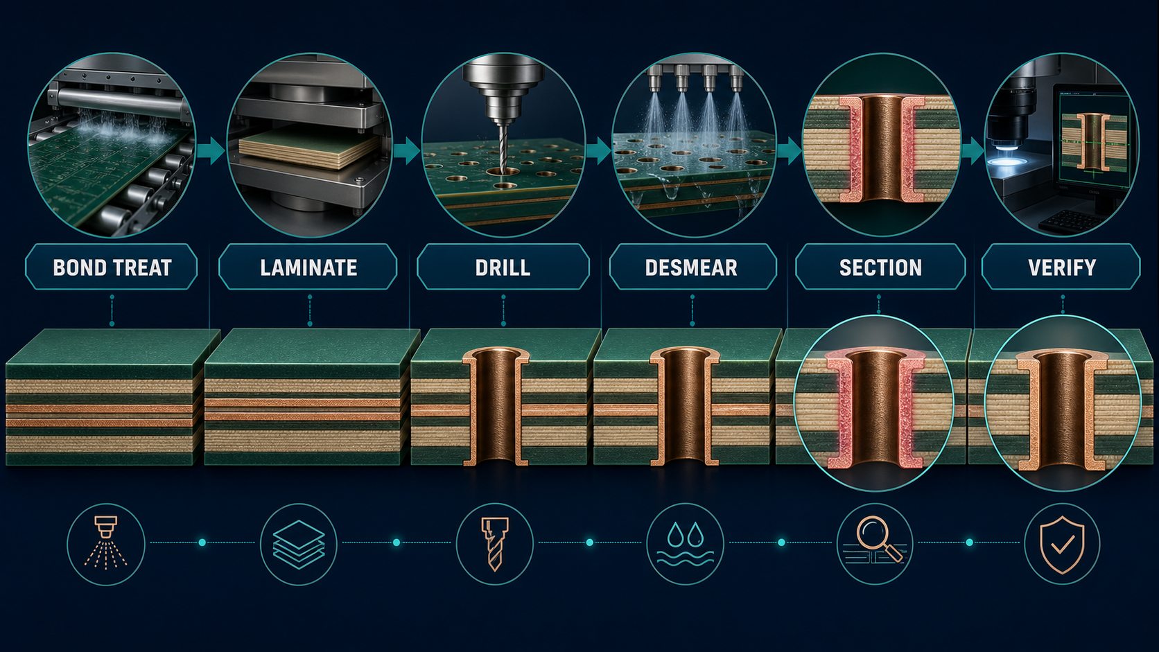
What Pink Ring Does and Does Not Prove About Reliability
Pink ring proves that the interface appearance changed; it does not by itself prove delamination, an open circuit or future field failure. Reliability significance depends on the remaining bond, associated separation, ring extent, product requirement, environment and evidence from representative samples.
Look for related conditions such as inner-layer separation, resin recession, barrel cracks, plating voids or laminate damage. If none is present, the disposition may differ from a section showing a visible gap or failed interconnect. Use the governing customer and product specification rather than a threshold copied from an unrelated source.
Electrical test cannot characterize the bond interface. A board may pass continuity while a structural concern remains. Conversely, a pink appearance does not establish an electrical defect without supporting evidence.
Need an evidence-based review of a pink-ring finding?
Send the full microsection images, stackup, material callout, bond-treatment route, drill data, desmear history and lot map. EBest Circuit can identify missing evidence before a disposition or corrective rebuild.
Inspection Evidence Needed Before Lot Disposition
A defensible report connects each image to a board, lot, location and preparation condition. Include:
- part number, revision, production lot and panel position;
- stackup, affected layer and hole type;
- full-hole overview plus detailed images with scale;
- section orientation and confirmation that the cut is centered;
- ring extent around the circumference and at each layer;
- sample count and number of affected holes;
- associated separation, void, crack or laminate observations;
- thermal conditioning and sample-preparation history;
- comparison with a known-good or unaffected location;
- acceptance reference and named disposition authority.
The PCB microsection analysis guide provides a broader framework for preparing sections and turning images into an actionable report.
A Root-Cause Sequence for Pink Ring Findings
- Confirm: repeat questionable sections and rule out polishing or etching artifacts.
- Map: record affected layers, hole sizes, panel positions and frequency.
- Contain: preserve lots and unused samples while risk is evaluated.
- Correlate: compare treatment, layup, press, drill and desmear batches.
- Separate: identify any associated delamination, voids or interconnect defects.
- Hypothesize: rank causes that match both morphology and process pattern.
- Trial: change one controlled contributor where practical.
- Verify: rebuild and inspect representative coupons/boards using the agreed sequence.
If the feature clusters by one treated-inner-layer batch, investigate upstream. If it follows a drill tool or hole size, examine mechanical preparation. If it follows one desmear load or panel position, chemistry uniformity becomes more likely. Correlation guides the trial; it does not replace verification.
Containment While the Cause Is Still Open
Containment should prevent uncontrolled shipment and preserve the evidence needed for the permanent fix.
- Define suspect lot boundaries and downstream locations.
- Segregate suspect, screened, accepted and rebuilt material.
- Maintain panel, material, treatment, press, drill and chemistry traceability.
- Reserve unsectioned samples from affected and comparison groups.
- Document any temporary screen and its detection limits.
- Prevent extra thermal or chemical exposure from changing the evidence.
- Set the responsible disposition authority and next review point.
Do not call screening a corrective action. A screen may remove visible extremes while leaving the cause unchanged.
Cause-Specific Corrective Actions and Verification
| Confirmed pattern | Corrective direction | Verification evidence |
| Bond-treatment batch correlation | Restore chemistry, rinsing, loading and hold-time controls | Controlled treated-panel comparison and sections |
| Lamination/load correlation | Correct material, layup, vacuum or press-cycle control | Actual press chart plus mapped rebuild sections |
| Drill-tool/hole-size correlation | Adjust tool life, parameters or stack conditions | Controlled drill trial through plating and section |
| Desmear-load correlation | Correct bath control, exposure and uniformity | Chemistry records plus representative hole sections |
| Preparation artifact | Correct mounting, polishing or etching | Independent repeat sections without the false feature |
Verification should reproduce the relevant construction and process route. One clean microsection from an unrepresentative coupon is weaker than a mapped sample across the corrected build.
PCB Data and Records to Send for Engineering Review
- Gerber or ODB++, controlled fabrication drawing and revision;
- stackup, laminate/prepreg and copper-weight callouts;
- NC drill files and drill table;
- acceptance class or customer-specific requirement;
- full-resolution micrographs with sample identification;
- lot/panel map and observed frequency;
- bond-treatment, lamination, drilling and desmear records;
- thermal, assembly or rework history;
- current containment status and response deadline;
- quantity and target delivery if a corrective build is required.
Turn the finding into a controlled PCB build plan
Include design data, material/stackup, hole information, acceptance requirement and the original inspection package so manufacturing and verification requirements can be reviewed together.
FAQ About PCB Pink Ring
Is PCB pink ring the same as a pink circuit board?
No. Pink ring is a local multilayer-interface condition around a drilled hole. A pink PCB normally refers to an intentional solder-mask color.
Does pink ring mean the annular ring is too small?
No. Annular-ring breakout concerns pad geometry and registration. Pink ring concerns the treated inner-layer copper/resin interface.
Can pink ring be seen from the board surface?
It may be suspected during destructive inspection, but a prepared cross-section is normally needed to understand affected layers and associated conditions.
Is every pink ring rejectable?
No universal disposition applies. Use the governing requirement, measured extent, associated defects, representative sampling and product risk.
Does pink ring always cause electrical failure?
No. The color change alone does not establish an open or short. It must be evaluated as part of the structural and process evidence.
Can desmear cause pink ring?
Hole-preparation chemistry can contribute, but bond treatment, lamination, drilling and material conditions must also be correlated before assigning cause.
Can microsection preparation create a misleading ring?
Yes. Polishing and etching can change contrast or produce artifacts, so questionable findings should be repeated with controlled preparation.
What should be measured?
Record affected layers, circumferential extent, radial distance, frequency and any associated gap, void or laminate damage using the agreed method.
What records are most useful?
Bond-treatment, press, material, drill and desmear traceability are especially useful when paired with a panel map and full micrographs.
How is prevention verified?
Use a controlled build with the confirmed correction, then repeat the agreed sectioning and sampling plan across representative locations.
Final Prevention Checklist
- Define pink ring separately from breakout, measling and plating defects.
- Control inner-layer treatment, handling and time to lamination.
- Verify material, layup and actual press-cycle records.
- Control drill tool life and hole-preparation chemistry.
- Map findings by layer, hole, panel and lot.
- Use representative microsections and an agreed acceptance basis.
- Link the correction to confirmed cause evidence.
- Verify a controlled rebuild before closing the action.
Request a multilayer PCB engineering and quotation review.
Send Gerber or ODB++, stackup, drill files, material callout, micrographs, process history, quantity and target delivery to sales@bestpcbs.com, or use the PCB quote form. EBest Circuit will identify missing evidence and align fabrication and inspection requirements before production.
You may also like








Tags: Multilayer PCB, pcb failure analysis, PCB Quality Control