





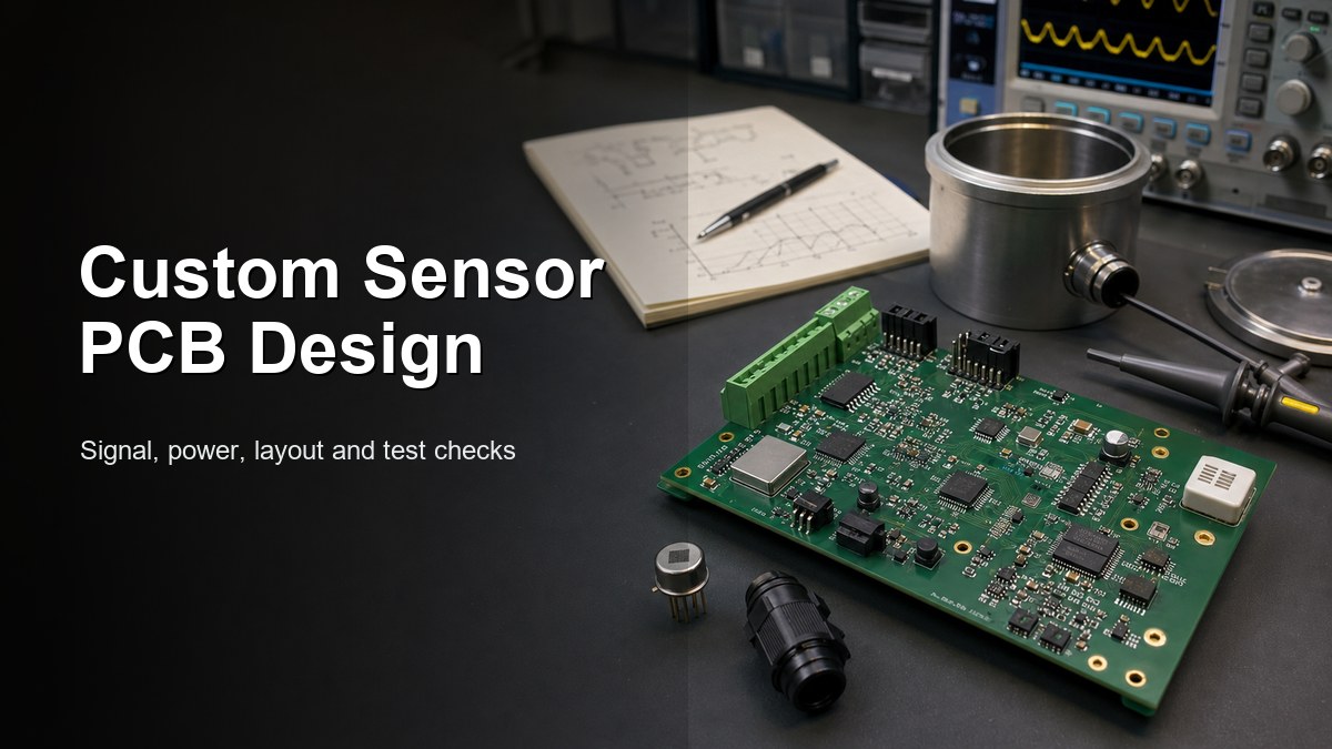
Custom PCB design for sensors should be reviewed around signal accuracy, low-noise power, grounding, connector placement, calibration access, test points, environmental protection and production-ready RFQ files. A sensor PCB is not only a small carrier board for a sensing element. It is the interface between the real world and the electronics that must read that signal consistently.
This guide is written for engineers and buyers preparing a custom sensor PCB or sensor PCBA for industrial devices, IoT products, environmental monitoring, equipment controls, medical-adjacent instruments, automotive modules or field equipment. It focuses on manufacturable board design and supplier review, not on selecting one specific sensor IC.
What does custom PCB design for sensors need to solve?
A sensor PCB needs to preserve the signal the sensor produces while surviving the mechanical, electrical and environmental conditions around the final product. The board may measure temperature, pressure, humidity, light, motion, gas, current, position or vibration, but the design checks follow a similar pattern: protect the signal path, control noise, provide stable power and make the board testable.
Low-current analog sensors may need guarded routing, short high-impedance traces and careful leakage control. Digital sensors may need clean I2C, SPI, UART, CAN, RS-485 or wireless module routing. Compact sensor products may use an HDI PCB when the enclosure is tight and the connector, MCU, RF section and sensing element compete for space.
| Sensor board area | PCB design check | Buyer or engineer risk |
|---|---|---|
| Signal path | Short routing, shielding, filtering, impedance or guard traces when needed | Noise, drift or unstable readings can hide the real sensor output |
| Power supply | Low-ripple rails, local decoupling, regulator heat and startup behavior | Power noise can show up as false measurement changes |
| Grounding | Analog/digital return paths, chassis connection and cable shield plan | Ground loops or poor return paths can create hard-to-debug faults |
| Environment | Coating, enclosure interface, sensor exposure window and connector sealing | Humidity, dust, chemicals or vibration can change readings or damage the board |
| Production test | Test pads, calibration points, programming access and fixture clearance | Good prototypes can become slow or inconsistent in volume builds |
Which sensor applications need a custom PCB?
A custom PCB is useful when the sensor board must fit a product enclosure, meet a specific noise target, connect to a harness, support calibration or survive a defined operating environment. Evaluation boards are useful for early testing, but they rarely match the size, connector, grounding, power and protection requirements of the final product.
Common examples include environmental sensor nodes, industrial monitoring modules, battery and charger sensors, flow meters, load-cell interfaces, motor feedback boards, optical sensor boards, wearable sensor modules and equipment health monitoring electronics. Many designs can use an FR4 Printed Circuit Board. High-frequency, wireless or antenna-connected sensor products may need RF material decisions, controlled routing or a review against an RF PCB capability page.
How should low-noise layout be planned?
Low-noise sensor layout starts with floorplanning: keep the sensor front end, reference, ADC, filter, connector and noisy switching circuits in controlled zones. A layout can pass a simple connectivity check but still produce unstable data if switching regulators, antennas, motors, relays or long cable inputs couple noise into the measurement path.
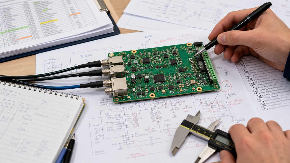
Place the sensor and analog front end close together when the signal is small. Keep high-current switching loops away from sensitive inputs. Use a continuous reference plane where possible, and avoid splitting a return path under critical traces without a clear reason. For cable-connected sensors, review ESD, surge, filtering and shield termination before release. If the design uses a flex tail or adhesive-mounted sensing element, confirm bend area, stiffener position and assembly handling early.
What power and grounding checks matter most?
Power and grounding checks should answer whether the sensor reading stays stable during startup, load changes, communication bursts and nearby switching events. Sensors that look accurate on a bench supply can become noisy when they share power with radios, relays, motors, LEDs, heaters or long cable harnesses.
Ask the designer or supplier to review regulator choice, decoupling placement, reference voltage routing, ground return, cable shield strategy and any required isolation. If a sensor board includes both sensitive analog inputs and digital communication, the layout should support both signal integrity and production assembly. When the order includes SMT, through-hole parts, connectors and final inspection, discuss the project as a Prototype PCB Assembly or production PCBA job instead of a bare PCB only.
How should connectors, cables and enclosures be designed?
Sensor PCB reliability often depends on connector orientation, cable strain relief, enclosure clearance and how the sensor is exposed to the measured environment. A board can be electrically correct but hard to assemble if the cable exits the wrong side, the sensor window does not align, or the test pads are blocked by the housing.
Before fabrication, compare the PCB outline with the enclosure model, mounting bosses, gasket, sensor opening, cable routing and service access. For field devices, define whether the board needs conformal coating, potting, a vented enclosure, connector sealing or a separate daughterboard. If the supplier is expected to assemble the PCB into a housing or harness, treat the RFQ as a Box Build Assembly discussion.
When do flex or rigid-flex sensor boards make sense?
Flex and rigid-flex sensor boards make sense when the sensing element must sit away from the main electronics, bend around a shape, reduce connector count or fit a compact enclosure. They are common in wearables, medical-adjacent devices, compact industrial sensors, optical modules, probes and adhesive-mounted sensing assemblies.
Flex is not a shortcut around mechanical design. Bend radius, copper direction, stiffener location, adhesive choice, strain relief and assembly sequence still need review. If a sensor product uses a flexible circuit, compare the design against a proven custom flex PCB design checklist before ordering production tooling.
What should be included in the sensor PCB test plan?
The test plan should prove that the board can be fabricated, assembled, programmed, calibrated and checked repeatedly before it reaches the final product. For sensor PCBA, continuity alone is usually not enough. The test may need known input conditions, reference measurements, firmware loading, communication checks and pass/fail limits.
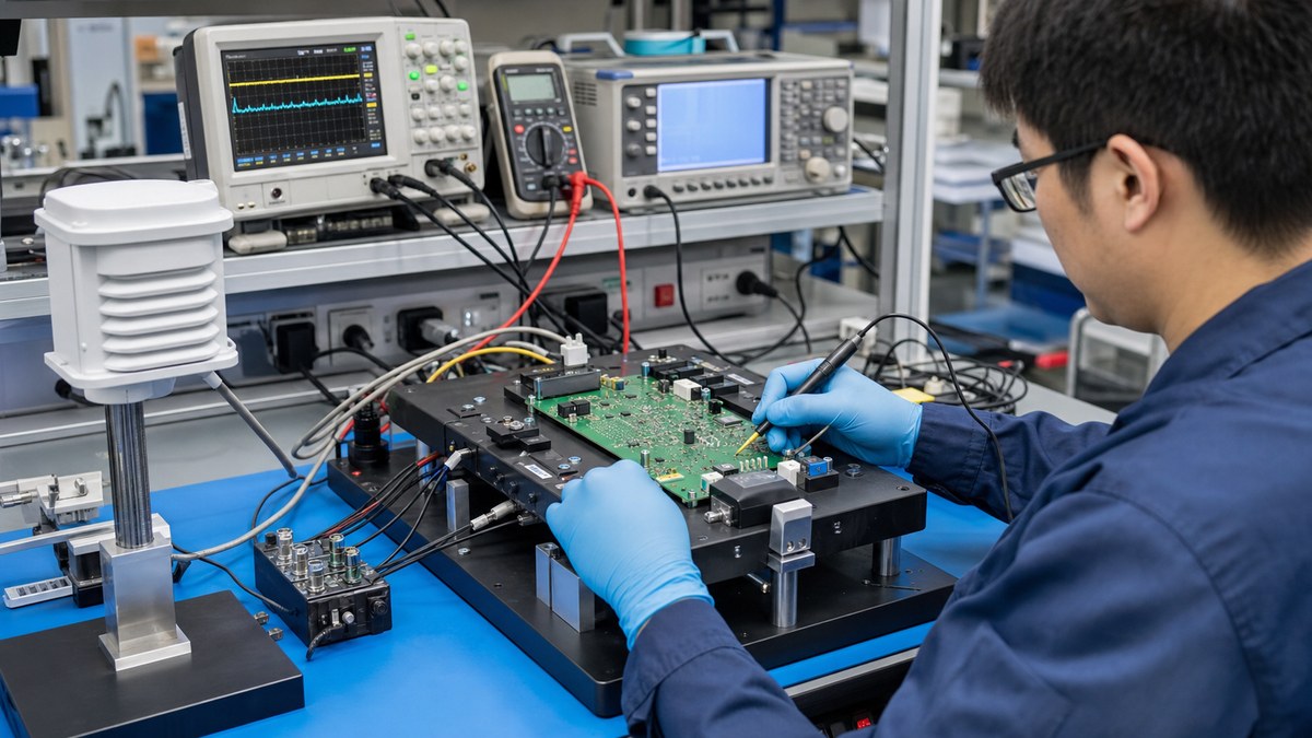
Add test pads for power rails, ground, programming, communication lines and critical analog nodes. Keep them reachable after assembly and enclosure installation. If calibration is needed, define the calibration input, equipment, firmware state and acceptable tolerance. A supplier’s PCB test equipment and fixture planning should be discussed before volume production, not after failed boards appear.
RFQ checklist for custom sensor PCB design
A strong RFQ package lets the supplier review sensor accuracy, manufacturability, assembly risk and test coverage before quoting price and lead time. Send controlled files instead of screenshots or partial exports.
- Gerber files, drill files, netlist and controlled revision number.
- Schematic, stackup, copper weight, board thickness and surface finish requirement.
- Sensor type, expected signal range, accuracy goal and calibration requirement.
- Power input range, current load, regulator notes and any battery or charger interface.
- Connector, cable, enclosure, coating, potting or gasket information.
- BOM, approved alternates, centroid file and assembly drawing for PCBA.
- Programming method, firmware loading requirement and functional test criteria.
- Environmental notes such as temperature, humidity, vibration, dust, chemicals or outdoor exposure.
Supplier questions buyers should ask
The best supplier questions force a real DFM and test review instead of a generic board price. Use them before approving the first build.
- Which parts of this sensor design create the highest layout or assembly risk?
- Are the sensor, connector and enclosure clearances consistent with the mechanical file?
- Do any analog inputs need additional spacing, guarding, shielding or cleaning controls?
- Are the test pads reachable after assembly and enclosure installation?
- Which components have sourcing risk or need approved alternates?
- Can the test fixture simulate or verify the sensor input reliably?
- What should change before moving from prototype to pilot production?
Sensor boards often depend on stable parts. If a project uses specialized sensor ICs, connectors, filters, references or wireless modules, involve Component Sourcing early so substitutes do not change measurement behavior without engineering approval.
FAQ
What is custom PCB design for sensors?
Custom PCB design for sensors means designing a circuit board around a sensing element, signal chain, power system, connectors, firmware access and test plan for a specific product. The goal is to read the sensor accurately and build the board repeatedly, not just connect a sensor IC to a controller.
Does every sensor PCB need a four-layer board?
No. Simple low-speed digital sensor boards may work on two layers when routing, power and grounding are clean. Mixed-signal, wireless, compact or low-noise sensor boards often benefit from four or more layers because a stable reference plane and controlled return paths reduce layout risk.
What causes noise in sensor PCB readings?
Common causes include unstable power rails, poor grounding, long high-impedance traces, switching regulator noise, nearby motors or relays, cable pickup, weak shielding, poor filtering and bad test setup. The fix depends on the sensor type and signal level, so schematic and layout review should happen before fabrication.
What files are needed for a sensor PCB quote?
Send Gerber and drill files, schematic, stackup, board drawing, BOM, centroid file, assembly drawing, enclosure notes and test requirements. If calibration, coating, potting, firmware loading or box build is required, include those details in the first RFQ.
Can a PCB supplier improve sensor accuracy?
A PCB supplier can help with manufacturability, material choice, assembly quality, inspection and repeatable testing. Accuracy still depends on the sensor IC, circuit design, layout, calibration method, firmware and operating environment. Treat supplier feedback as one part of the engineering review.
Conclusion
Custom PCB design for sensors should start with the measurement problem, not with board price. Define the signal, power rails, grounding, enclosure, connector, calibration and test plan before production files are released. Then ask the supplier to review manufacturability and assembly risk against the real use case. That process gives the sensor board a better chance of producing stable readings in the final product.
You may also like






Tags: Custom PCB, PCB Assembly, pcb design, PCB testing, Sensor PCB