





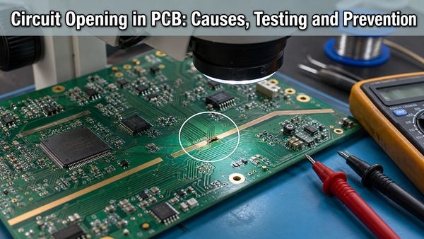
Circuit opening in a PCB means that a conductive path intended to carry power or a signal has been interrupted. The affected branch carries no useful current, although voltage may remain on the source side of the break. On a bare board, the fault may be a broken trace, via-barrel discontinuity or missing inner-layer connection. On an assembled board, it may be an unsoldered terminal, lifted lead, cracked joint or failed component.
What Does Circuit Opening Mean in a PCB?
In PCB work, circuit opening describes a loss of electrical continuity between points that should belong to the same net. The phrase is commonly used for an open circuit, open connection or open-net defect. It should not be confused with an intentionally open switch: both stop current, but only the unintended condition is a manufacturing or reliability fault.
The physical break can be obvious, such as a severed surface trace, or hidden inside a plated through-hole, multilayer interconnect, package termination or solder joint. A net may also behave as open only under heat, vibration or board flex. That intermittent condition can pass a room-temperature bench check and fail later in operation.
What Electrical Changes Occur When a Circuit Opens?
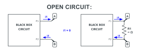
An ideal open circuit has zero current and infinite resistance. A real fault usually has resistance beyond the instrument range or a contact that changes between very high and lower resistance. The voltage behavior depends on where the break occurs and how the circuit is referenced.
- Current: useful branch current falls to zero because the loop is incomplete.
- Resistance: a powered-off continuity or resistance test normally shows OL or no beep across a complete break.
- Voltage: source voltage can appear across an energized break, so an open circuit is not automatically safe to touch.
- Signal state: a disconnected input may float, be forced by a pull-up or pull-down, or show coupled noise.
- AC and high-frequency behavior: parasitic capacitance can pass a small displacement current even though DC continuity is absent.
A high-impedance voltmeter can therefore display voltage at an open node. That reading does not prove the path can deliver current; the voltage may collapse when a defined load is connected.
What Does an Open Circuit Diagram Show?
An open circuit diagram shows a gap in the intended current loop. In a simple source-switch-load circuit, opening the switch separates the contacts, sets branch current to zero and places most of the source voltage across the gap. For a PCB fault diagram, the gap should be marked on the specific net rather than drawn as a generic disconnected wire.
A useful diagnostic drawing includes the source, return path, expected load, test points and the suspected break. Net names and reference designators make it possible to transfer the diagram to the actual board without guessing which conductor belongs to the failed function.
What Causes Circuit Opening in Bare PCB Fabrication?
Bare-board opens originate when the designed copper connection is missing, too thin, fractured or not joined between layers. The defect mechanism can usually be narrowed by its geometry and repetition pattern.
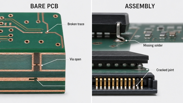
- Imaging or resist defects: missing artwork, debris, resist damage or poor development can remove part of a conductor.
- Excessive local etching: a narrow trace can be necked down or fully separated. The related PCB etching process must be checked against artwork, copper weight and panel position.
- Via or plated-hole discontinuity: drilling damage, desmear problems, poor activation, plating voids or barrel cracks can interrupt an interlayer path.
- Inner-layer registration or lamination damage: a pad-to-hole connection may be lost, or an inner conductor may crack during processing.
- Handling and routing damage: scratches, depaneling stress or edge breakout can sever traces after imaging and plating are complete.
If the same feature fails on every panel, data or tooling should be reviewed first. If failures repeat at one conveyor or panel position, imaging, spray, plating or handling equipment is more likely. Random isolated opens need microscopy and cross-section evidence before the process is adjusted.
What Causes Open Circuits During PCB Assembly?
Assembly opens occur when a valid bare-board net is not electrically joined through the installed component or connector. The failure may be visible, hidden beneath a package or mechanically intermittent.
- Insufficient or missing solder paste caused by a blocked aperture, poor print alignment or unsuitable stencil design.
- Non-wetting, poor flux activation or an unsuitable reflow profile that leaves the terminal electrically isolated.
- Tombstoning, lifted leads or package warpage that separates one terminal during reflow.
- Cracked solder joints, component terminations or PCB pads after thermal cycling, impact, vibration or excessive board strain.
- Connector pins that are recessed, bent, contaminated or not fully seated.
- Missing, damaged or internally open components, including fuses and inductors.
For BGA and QFN packages, an open must not automatically be described as a solder void. Non-wetting, head-in-pillow, pad cratering, package warpage and interconnect cracking require different evidence and corrective action.
Which Symptoms Indicate Circuit Opening?
Circuit opening symptoms depend on the affected net. A power-path open can disable the whole board, while a signal-path open may affect only one channel, sensor, communication line or output.
- No power at a downstream rail even though the source voltage is present.
- A missing clock, control or data signal after a specific component or connector.
- An input stuck high, stuck low or unstable because its intended driver is disconnected.
- A function that returns when the board, cable or connector is pressed or flexed.
- Failure only during warm-up, cooling, vibration or high-current operation.
- A continuity reading that changes when a joint or package is mechanically stressed.
These symptoms identify the affected function, not the physical root cause. The schematic, netlist and board layout are needed to convert the symptom into a controlled test path.
How Do You Find an Open Circuit on a PCB?
Start from the failed function and trace one net at a time. Random probing can miss parallel paths or damage sensitive nodes.
- Review the schematic, net names, connector pinout and expected power sequence.
- Remove power and discharge stored energy before using continuity or resistance mode.
- Inspect connectors, fuses, component leads, test pads, vias and high-strain board areas under magnification.
- Check continuity between known endpoints, then divide a long path into smaller sections using accessible test points.
- If continuity is present but the function still fails, apply power safely and compare voltage or waveform measurements before and after each section.
- Use package-specific inspection when the suspected connection is hidden.
In-circuit readings can be affected by parallel components, protection devices and semiconductor junctions. A no-beep result is useful only when the expected path and meter threshold are understood.
How Should Continuity and Voltage Tests Be Used?
Continuity testing confirms whether a low-resistance path exists while the circuit is de-energized. Voltage testing shows how an energized circuit behaves. They answer different questions and should not be interchanged.
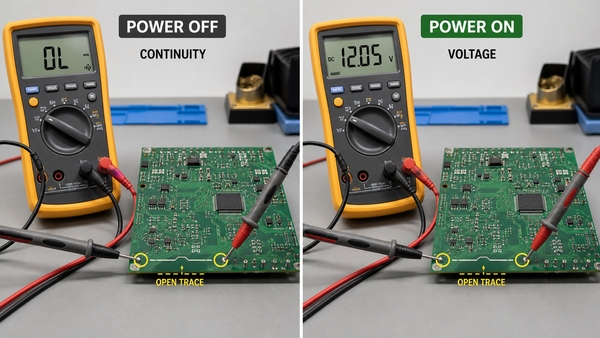
| Test | Power State | Useful Result | Important Limit |
|---|---|---|---|
| Continuity | Off | Finds a complete low-resistance path | Meter thresholds vary; parallel paths can beep |
| Resistance | Off | Shows OL, unstable contact or abnormal resistance | Capacitors and semiconductors can change the reading |
| DC voltage | On | Shows where expected potential disappears | An open node may still show phantom or unloaded voltage |
| Oscilloscope | On | Locates missing or distorted dynamic signals | Probe reference and loading must be controlled |
Never use resistance or continuity mode on an energized board. When voltage remains on both sides of a suspected open, compare the measurement under a known safe load and check whether the node is floating or capacitively coupled.
How Are Hidden and Intermittent Open Circuits Located?
Hidden opens require a test that matches the failure condition. A static room-temperature measurement cannot reliably expose a crack that opens only when materials expand or the board bends.
- X-ray inspection: useful for package alignment, solder shape and some hidden joint anomalies, but not every planar crack is visible.
- Cross-section analysis: confirms via-barrel, inner-layer, pad and solder-joint structure destructively.
- Thermal stimulation: monitor continuity or function while temperature changes within controlled limits.
- Mechanical stimulation: apply defined board flex or vibration while recording resistance; uncontrolled hand bending can create new damage.
- Time-domain reflectometry: locates impedance discontinuities along long cables or transmission paths by distance.
- Four-wire measurement: resolves small resistance changes in contacts and joints before a complete open develops.
Record temperature, load, fixture position and applied stress when the fault appears. Without repeatable conditions, an intermittent open may be reported as “no fault found” even when the defect remains.
How Do PCB Factories Detect Circuit Opening Defects?
No single inspection method covers every open. A manufacturing test flow combines image comparison, electrical continuity and functional evidence at the stage where each defect is detectable.
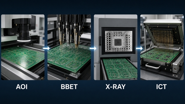
- AOI: finds missing copper, neck-downs, solder defects and displaced components that are optically visible.
- Bare-board electrical test: compares continuity and isolation against the approved netlist before assembly.
- SPI and post-reflow AOI: screen paste deposition, placement and visible solder-joint conditions.
- X-ray: examines hidden package and through-hole structures where optical access is limited.
- ICT: checks nets, components and pin connections through a fixture and test program. The in-circuit testing guide explains its coverage and limitations.
- FCT: verifies that the assembled board operates under defined inputs, loads and interfaces.
EBest Circuit (Best Technology) can support PCB fabrication and PCB assembly projects with process review and suitable inspection planning. The required test coverage should follow the design, access to test points, package types and reliability conditions rather than a generic test list.
What Is the Difference Between an Open, Closed and Short Circuit?
The three states differ by whether the intended path is complete and whether an unintended low-resistance path exists.
| Condition | Path | Current | Resistance | Typical PCB Example |
|---|---|---|---|---|
| Open | Intended path interrupted | Zero in the affected branch | Very high or unstable | Cracked trace or unsoldered lead |
| Closed/normal | Intended loop complete | Defined by the load | Expected circuit value | Valid powered or signal connection |
| Short | Unintended low-resistance path | Potentially excessive | Very low | Solder bridge between nets |
An open and a short can occur in the same assembly but require different localization methods. A short is found by identifying the unwanted connection; an open is found by identifying where the required connection disappears.
How Can Circuit Opening Defects Be Prevented?
Prevention requires controls at design, fabrication, assembly and verification stages. Testing alone can screen defects but cannot correct a weak design margin or unstable process.
- Use conductor widths, annular rings, pad geometries and via structures compatible with the selected copper weight and fabrication process.
- Protect neck-down traces and connections near board edges, slots, connectors and depaneling routes.
- Balance stencil apertures, pad thermal mass and component orientation for stable solder paste transfer and reflow.
- Control board support during assembly, connector insertion, screw fastening and test fixture contact.
- Add accessible test points to critical rails, interfaces and long signal paths.
- Match materials and joint design to thermal cycling, vibration and mechanical strain requirements.
- Use fabrication AOI and netlist electrical testing before assembly, then apply assembly inspection and electrical tests appropriate to package visibility.
FAQ About Circuit Opening
What is another word for an open circuit?
Depending on context, engineers may use open connection, open net, discontinuity, broken circuit or circuit opening. On a PCB defect report, the net name and physical location are more useful than the general label alone.
How do you open a circuit intentionally?
A switch, relay, transistor in its off state, fuse or circuit breaker can intentionally interrupt a current path. The device rating must match the voltage, current, load type and switching transient.
Can current flow through an open circuit?
Ideal DC current is zero. In real circuits, leakage and parasitic capacitance may allow extremely small currents, especially at high frequency, but the path cannot carry its intended current.
Can an open circuit still have voltage?
Yes. Source voltage can appear across the break or at a floating node. Treat the circuit as energized until voltage is measured and the energy source is safely isolated.
What is the most common PCB circuit opening cause?
There is no universal single cause. Bare boards commonly involve conductor or via discontinuity; assembled boards commonly involve solder, terminal or mechanical connection failures. Failure location and repetition pattern should determine the investigation.
Conclusion
Circuit opening faults interrupt required power or signal paths, but the physical cause can originate in copper imaging, via plating, soldering, component contact or later mechanical and thermal stress. Reliable diagnosis starts with the schematic and netlist, separates powered and unpowered tests, and applies hidden-joint or intermittent-fault methods only where needed.
For PCB fabrication or PCBA support, contact EBest Circuit (Best Technology) at sales@bestpcbs.com.
You may also like






Tags: circuit opening, open circuit, PCB defects, PCB testing, PCBA troubleshooting