PCB testing is not a single inspection performed at the end of production. It is a sequence of checks used to verify the bare circuit board, soldering process, component placement, electrical connections, and final product operation.
A bare PCB may pass an electrical continuity test but still develop a soldering or component failure after assembly. Likewise, an assembled board may look perfect under AOI yet fail when power is applied. A reliable testing plan therefore combines several methods rather than relying on one machine.
This guide explains the complete PCB testing procedure, including bare-board electrical testing, SPI, AOI, X-ray, flying probe, ICT, functional testing, and reliability qualification. It also shows how engineers and buyers can choose an appropriate test strategy for prototype PCB testing, small batches, and mass production.
What Is PCB Testing and What Does It Verify?
PCB testing is the process of finding manufacturing defects and confirming that a circuit board meets its electrical, mechanical, and functional requirements.
The term covers 2 different production stages.
Bare PCB Testing
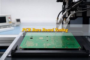
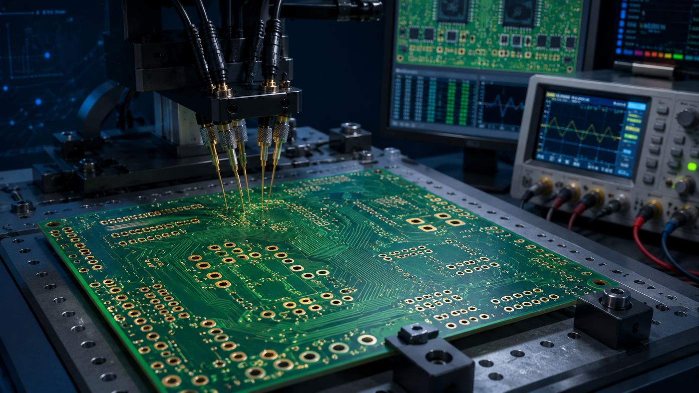
Bare PCB testing is performed before components are mounted. Its main purpose is to verify the manufactured interconnections against the design netlist.
It can identify:
- Open circuits
- Short circuits
- Incorrect net connections
- Excessive conductor resistance
- Poor plated-hole continuity
- Isolation problems between unrelated nets
IPC-9252 provides guidance for selecting test levels, analyzers, test data, parameters, and fixtures for unpopulated printed boards.
However, a bare-board electrical test does not verify component values, solder quality, firmware, or final product operation.
PCBA Testing
PCBA testing is performed after solder paste printing, component placement, reflow, through-hole assembly, or final integration.
It can verify:
- Solder paste volume and alignment
- Component presence and orientation
- Solder-joint quality
- Resistor, capacitor, diode, and other component values
- Opens and shorts after assembly
- Power-rail behavior
- Communication interfaces
- Firmware programming
- Inputs, outputs, sensors, displays, relays, and other functions
The distinction is important. A PCB manufacturer may offer 100% bare-board electrical testing, while PCBA testing may require customer-supplied test procedures, fixtures, firmware, golden samples, or functional limits.
Inspection, Electrical Testing, and Reliability Testing
These terms are related but not interchangeable.
Inspection examines physical workmanship. SPI, AOI, manual inspection, and X-ray belong to this category.
Electrical and functional testing applies measurements or operating conditions to determine whether circuits and components behave correctly. Flying probe, ICT, boundary scan, and FCT belong here.
Reliability testing evaluates whether a design or manufacturing process can survive repeated heat, humidity, vibration, current, or mechanical stress. It is normally used for qualification or sampling rather than as a production test for every board.
A strong test plan uses the right layer of verification at each production stage.
What Is the Standard PCB Testing Procedure?
The exact PCB testing process depends on the product, but a typical manufacturing sequence follows these stages.
Bare-Board Visual and Dimensional Inspection
Before electrical testing, the manufacturer checks:
- Board dimensions
- Hole size and location
- Surface finish
- Solder mask registration
- Legend alignment
- Annular rings
- Copper exposure
- Edge damage
- Bow and twist
Automated optical equipment may support this inspection, but some criteria still require operator review or dimensional measurement.
Bare-Board Electrical Test
The manufactured board is compared with the customer’s netlist or extracted CAD data.
A fixture-based tester or flying probe machine checks continuity within each net and isolation between unrelated nets. High-voltage or low-resistance requirements should be stated in the fabrication drawing or purchase specification rather than assumed.
This step confirms that the copper network is electrically correct before assembly begins.
Solder Paste Inspection
After solder paste printing, SPI measures paste deposits before components are placed.
Typical checks include:
- Paste height
- Area
- Volume
- Offset
- Bridging
- Insufficient paste
- Excess paste
Catching printing defects at this point is efficient because the board has not yet entered reflow. Paste can often be cleaned and printed again without removing assembled components.
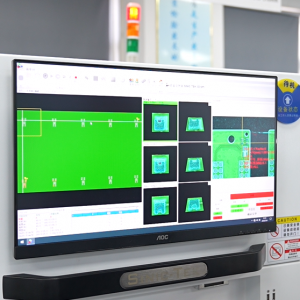
Pre-Reflow and Post-Reflow AOI
Pre-reflow AOI may check component presence, polarity, orientation, and placement offset.
Post-reflow AOI focuses on:
- Missing components
- Wrong components
- Polarity errors
- Tombstoning
- Lifted leads
- Visible solder bridges
- Insufficient or excessive solder
- Component displacement
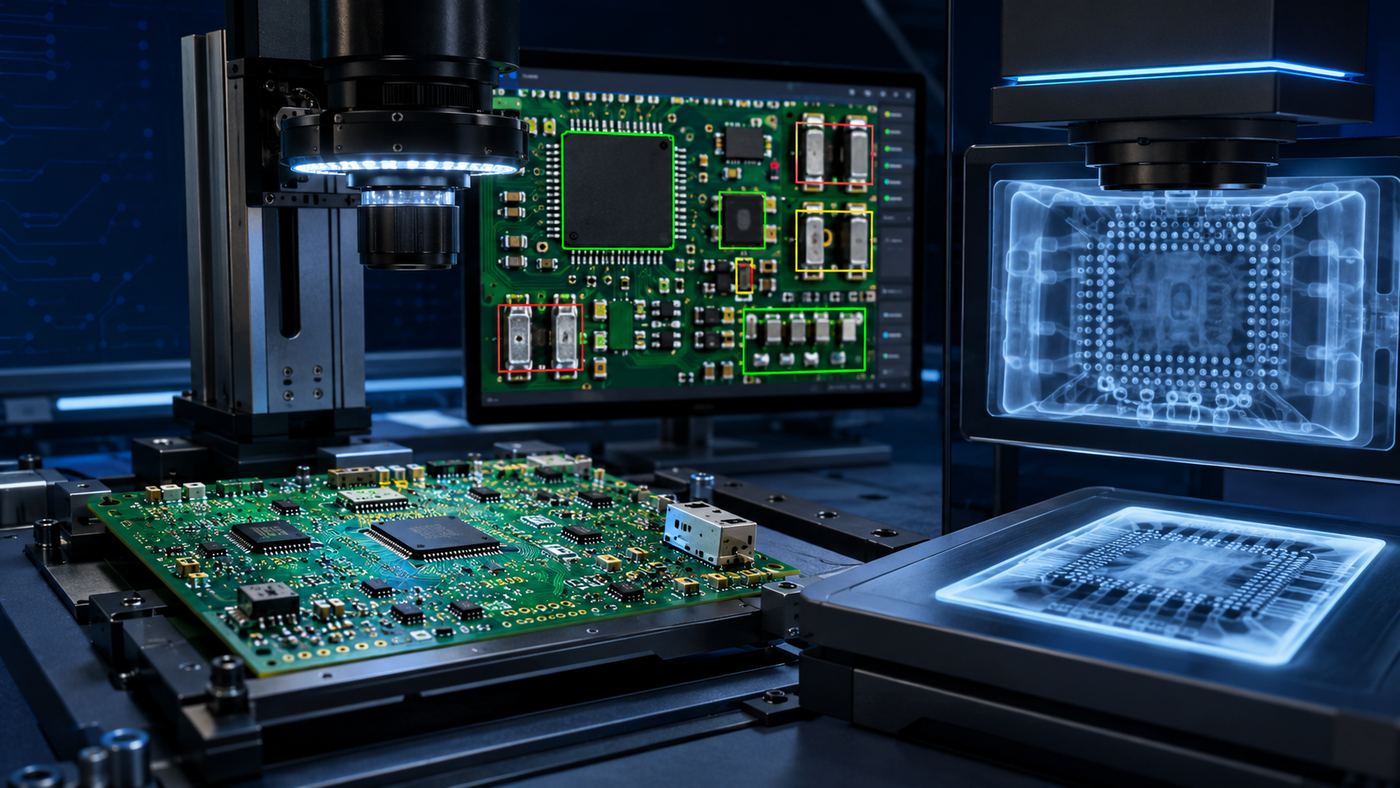
AOI is fast and suitable for inspecting visible features across an SMT production line. Modern inspection systems can measure and classify solder joints, although AOI does not prove that the circuit works electrically.
X-Ray Inspection
X-ray inspection is used where solder joints are hidden beneath a package or cannot be evaluated clearly by optical equipment.
Common applications include:
- BGA
- LGA
- QFN
- Bottom-terminated components
- Press-fit connections
- Through-hole barrel fill
- Power devices with thermal pads
X-ray can reveal internal voiding, bridges, insufficient solder, head-in-pillow defects, and irregular ball formation. In a coordinated inspection strategy, SPI addresses paste deposition, AOI covers visible assembly features, and X-ray examines internal structures.
ICT or Flying Probe Testing
After assembly inspection, the board may undergo an electrical structural test.
For prototypes and low-volume orders, flying probe testing is often selected because it does not require a dedicated bed-of-nails fixture.
For stable, higher-volume production, ICT can test many nodes rapidly through a custom fixture. It may check opens, shorts, component values, diode orientation, power rails, and other board-level characteristics.
Firmware Programming
Microcontrollers, FPGAs, EEPROMs, and other programmable devices may be loaded during ICT, functional testing, or a separate programming stage.
The programming process should control:
- Firmware revision
- Serial number
- Configuration data
- Calibration data
- Security keys, where applicable
- Programming verification
- Traceability records
In-system programming can also be integrated into an ICT platform, reducing separate handling steps.
Functional Circuit Testing
Functional circuit testing powers the PCBA and confirms that it performs its intended operations.
Depending on the product, FCT may measure:
- Input current
- Standby current
- Power-rail voltage
- Output voltage or current
- Signal frequency
- Communication ports
- Sensor response
- Motor or relay control
- Audio, display, LED, or wireless operation
- Protection and alarm functions
FCT is normally based on the product specification rather than a universal test program.
Reliability Sampling and Final Inspection
High-reliability products may require environmental or endurance testing during qualification, process validation, or lot sampling.
After testing, the manufacturer completes final visual inspection, cleaning verification, labeling, packaging, and test-record review.
The final release decision should be based on defined limits—not an operator’s informal judgment.
What Are the Main PCB Testing Methods?
No test method detects every possible defect. Each one has a distinct role.
Manual Visual Inspection
Manual inspection uses trained operators, magnification equipment, microscopes, and workmanship standards.
It is useful for:
- Low-volume prototypes
- Connector inspection
- Mechanical damage
- Hand-soldered joints
- Rework verification
- Areas that automated equipment cannot view clearly
Its main limitation is consistency. Detection depends on lighting, magnification, operator experience, and inspection time.
Manual inspection works best as a supplement, not the only quality gate.
Solder Paste Inspection
SPI is performed immediately after solder paste printing.
It is particularly valuable for fine-pitch components because paste volume directly affects the joint formed during reflow. Too little paste can produce opens or weak joints, while excessive or misaligned paste may create bridging.
SPI does not inspect the final solder joint. It controls the process before the joint is created.
Automated Optical Inspection
AOI captures images of the assembly and compares measured features with programmed rules, CAD data, or reference models.
Its strengths include:
- High inspection speed
- Repeatable coverage
- Early process feedback
- Automated defect classification
- Support for statistical process control
AOI is highly effective for visible defects but has limited access beneath BGA, LGA, QFN, and other bottom-terminated packages.
It also cannot confirm that a correctly oriented component has the correct internal value or that firmware is functioning.
Automated X-Ray Inspection
AXI uses X-rays to examine solder joints and conductive structures beneath components.
It is suitable for dense boards with:
- BGAs
- Area-array packages
- Hidden thermal pads
- Double-sided assemblies
- Complex through-hole joints
- High-reliability solder requirements
X-ray inspection provides structural evidence, but it does not replace electrical or functional testing. A solder joint may look acceptable while the circuit contains a wrong-value component or defective IC.
Bare PCB Electrical Testing
Bare-board electrical testing checks the manufactured copper network before assembly.
Two common approaches are used:
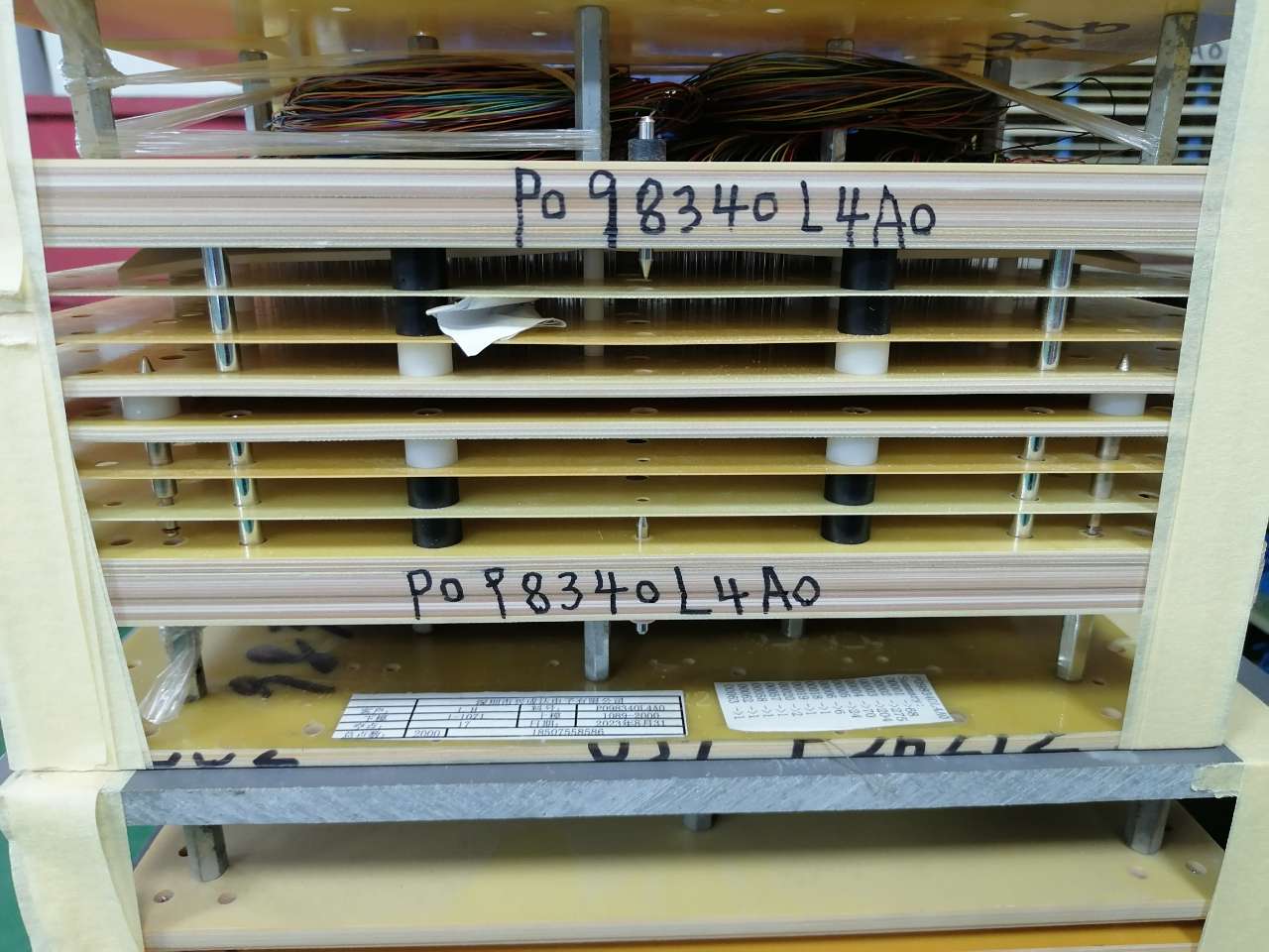
Fixture testing contacts many test points simultaneously through a dedicated fixture. It offers fast cycle times for repeated production.
Flying probe testing moves independent probes between pads, vias, and test points. It reduces tooling requirements and adapts more easily to revision changes.
The test data should be generated from controlled Gerber, ODB++, IPC-2581, netlist, or original CAD information. Testing against the wrong revision can produce a valid report for the wrong board.
Flying Probe Testing
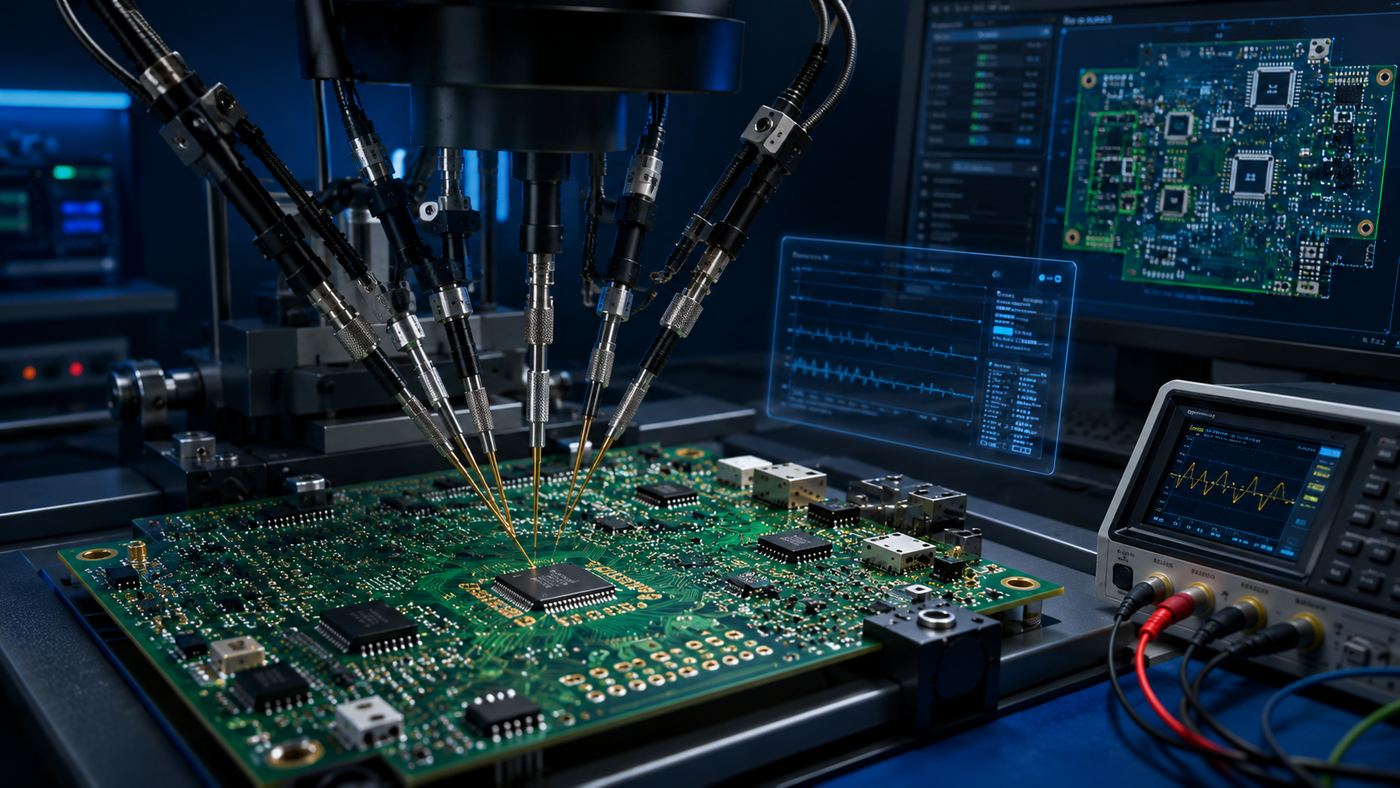
Flying probe testing uses programmable moving probes instead of a fixed bed-of-nails fixture.
It is well suited to:
- Engineering samples
- PCB prototypes
- Small batches
- Frequent design revisions
- Products with limited fixture budget
- New product introduction
Its main advantage is flexibility. Changes can often be handled by updating the test program rather than rebuilding a fixture.
The trade-off is test time. Probes contact test points sequentially, so a complex board may take longer than ICT.
Flying probe is not automatically superior for every prototype. Probe access, component density, board size, test coverage, and required measurements still affect feasibility.
In-Circuit Testing
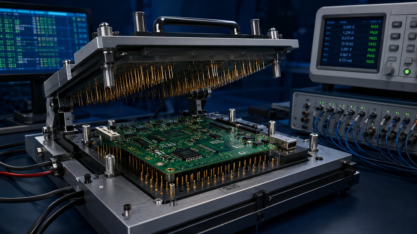
ICT uses electrical access to individual circuit nodes, commonly through a bed-of-nails fixture.
It can detect:
- Assembly opens and shorts
- Missing components
- Incorrect component values
- Reversed diodes
- Some incorrect IC placements
- Power-rail faults
- Certain soldering defects
ICT offers fast component-level fault isolation and is particularly effective in stable, higher-volume manufacturing. Complementary technologies such as boundary scan can extend coverage on dense boards.
The primary constraints are fixture cost, test-point access, program development, and maintenance after PCB revisions.
Boundary Scan Testing
Boundary scan uses test circuitry built into compatible ICs and is commonly associated with JTAG or IEEE 1149.x devices.
It can help test connections between digital devices where physical probes cannot reach every net.
Applications include:
- Dense BGA assemblies
- Processor and FPGA boards
- Digital interconnect verification
- Flash programming
- Limited-access designs
Boundary scan requires compatible components and correct scan-chain implementation. It does not provide full coverage for analog circuits or devices without boundary scan support.
It is often integrated with ICT rather than used as a complete replacement.
Functional Circuit Testing
FCT verifies the assembled board in an operating or simulated operating condition.
Unlike ICT, which focuses heavily on component-level faults, FCT asks a broader question: does the board perform its intended job?
A functional test may include:
- Power-up sequencing
- Current-consumption limits
- Analog input and output checks
- Digital I/O
- Communication protocols
- User controls
- Displays and indicators
- Load simulation
- Safety interlocks
- Calibration
FCT may identify that the board fails, but it may not isolate the exact defective component as quickly as ICT.
For this reason, ICT and FCT are often complementary. ICT supports diagnosis; FCT confirms system behavior.
Burn-In and Reliability Testing
Burn-in operates the PCBA for an extended period, sometimes under elevated temperature, repeated power cycling, or electrical load.
It may help expose early-life failures related to:
- Marginal components
- Poor solder joints
- Thermal instability
- Intermittent connections
- Power-device weakness
Burn-in is not needed for every consumer product. It is more appropriate when field failure carries a high cost or the product specification explicitly requires endurance screening.
What Equipment, Jigs, and Software Are Used for PCB Testing?
PCB testing equipment includes more than a single PCB testing machine. Fixtures, instruments, software, data limits, and traceability all affect the result.
| Test equipment | Main purpose | Typical production stage |
|---|---|---|
| Bare-board electrical tester | Opens, shorts, continuity, isolation | PCB fabrication |
| Flying probe tester | Fixtureless electrical measurements | Prototype or low-volume PCB/PCBA |
| SPI machine | Solder paste height, area, volume, offset | After printing |
| AOI machine | Visible component and solder defects | Before or after reflow |
| X-ray or AXI system | Hidden solder-joint inspection | After reflow |
| ICT system | Component-level electrical checks | PCBA production |
| Functional test jig | Product-specific operating test | Final PCBA stage |
| Oscilloscope | Waveform, timing, ripple, frequency | Debugging or FCT |
| DMM | Voltage, current, resistance, continuity | ICT, FCT, repair |
| Programmable power supply | Controlled board power and protection | FCT |
| Electronic load | Output loading and regulation tests | Power electronics |
| DAQ and switching system | Multi-channel automated measurements | Automated FCT |
PCB Testing Jigs
A test jig provides mechanical alignment and electrical connection between the test equipment and the board.
It may include:
- Pogo pins
- Connectors
- Pneumatic or manual clamping
- Relay switching
- Power supplies
- Loads
- Sensors
- Safety covers
- Barcode readers
- Status indicators
- Replaceable wear parts
A reliable jig must contact the board without damaging pads, bending the PCB, or creating unstable readings.
PCB Testing Software
Test software controls instruments, applies limits, records measurements, and generates pass/fail results.
A practical software architecture may include:
- Test-sequence control
- Instrument drivers
- Fixture control
- Firmware programming
- Limit files
- User permissions
- Error handling
- Serial-number tracking
- Data export
- MES integration
The software should store actual measurements where useful. A simple “PASS” record provides less diagnostic value than a report showing measured voltage, expected limits, test time, and failure location.
How Do You Choose the Right PCB Testing Method?
The best method depends on product risk, board design, production volume, and fault coverage.
| Method | Fixture required | Relative test speed | Best use | Main limitation |
|---|---|---|---|---|
| Visual inspection | No | Medium | Prototypes and workmanship checks | Operator-dependent |
| SPI | No product fixture | Fast | SMT paste-process control | Only checks printed paste |
| AOI | No electrical fixture | Fast | Visible SMT defects | Cannot inspect hidden joints or prove function |
| X-ray | No contact fixture | Medium | BGA, QFN, hidden joints | Structural inspection only |
| Flying probe | Usually no dedicated fixture | Slow to medium | Prototype and low-volume production | Longer cycle time |
| ICT | Yes | Very fast | Stable medium- or high-volume PCBA | Fixture cost and test-point demand |
| Boundary scan | No bed-of-nails fixture required | Fast | Dense digital boards | Requires compatible devices and design support |
| FCT | Usually yes | Application-dependent | Final product behavior | Program and fixture development |
| Reliability testing | Test coupons or chambers | Slow | Qualification and process validation | Not a routine per-board test |
For Prototypes
A practical PCB prototype test plan often includes:
- 100% bare-board electrical testing
- SPI and AOI during SMT assembly
- X-ray for BGA or hidden-joint packages
- Flying probe when electrical access allows it
- Basic power-up and functional verification
- Detailed engineering inspection of the first article
A costly ICT fixture may not be economical when the layout is still changing.
For Small-Batch Production
Small-batch products benefit from flexible methods:
- Flying probe
- Reusable connector-based functional jigs
- Modular DAQ systems
- Firmware programming
- AOI and targeted X-ray
- Golden-sample comparison
The goal is to gain useful coverage without excessive non-recurring engineering cost.
For Mass Production
Stable, high-volume products may justify:
- Dedicated ICT fixtures
- Automated board handling
- Inline AOI or AXI
- Automated firmware programming
- Parallel functional testing
- Barcode tracking
- MES data collection
- Statistical analysis of repeated failures
ICT has higher initial preparation costs, but its simultaneous fixture access can provide much faster throughput than sequential flying probes in volume production.
For High-Reliability Products
Automotive, medical, aerospace, industrial control, and power electronics may need a deeper strategy based on the product’s actual risk.
Possible additions include:
- Extended FCT
- High-voltage testing
- Leakage-current testing
- Boundary scan
- Thermal cycling
- Burn-in
- Vibration testing
- Conformal-coating inspection
- Lot traceability
- Calibration records
- Failure-analysis procedures
Industry certification alone does not define the product test. The drawing, quality plan, acceptance criteria, and customer specification must identify what is required.
How Does Design for Testability Improve PCB Test Coverage?
Design for testability, or DFT, makes the board easier to inspect, probe, program, diagnose, and verify.
It should begin during schematic and PCB layout—not after the production fixture has been ordered.
Add Accessible Test Points
Important nets may need test access, including:
- Ground
- Main input power
- Regulated power rails
- Reset
- Clock
- Communication buses
- Programming signals
- Critical analog signals
- Safety-monitoring signals
Test points should have enough diameter and clearance for the selected probe system.
Avoid Probe Collisions
Probe access can be blocked by:
- Tall components
- Connectors
- Shielding cans
- Heat sinks
- Board edges
- Closely spaced test points
- Components on the opposite side of a thin PCB
The fixture designer should review the final mechanical arrangement, not only the electrical netlist.
Plan Power Isolation
Some circuits need resistors, jumpers, relays, or removable links so individual power sections can be tested safely.
Without isolation, a short or wrong component in one section may affect measurements across several rails and make fault diagnosis difficult.
Provide a Stable Programming Interface
Programming pads or connectors should expose the required:
- Data
- Clock
- Reset
- Power
- Ground
- Boot-mode signals
The board should also provide a reliable method for confirming the programmed firmware version.
Consider Boundary Scan Early
Boundary scan must be supported by the chosen components and connected correctly in the schematic.
The scan chain, pull resistors, connectors, device order, and boot behavior should be reviewed before layout release.
Control Test Documentation
The manufacturer may need:
- Gerber or ODB++ data
- BOM
- Pick-and-place file
- Schematic
- Netlist
- Test-point list
- Firmware
- Programming instructions
- Test procedure
- Expected limits
- Connector pinout
- Golden sample
- Failure examples
Providing only a finished PCB layout is rarely enough to develop a comprehensive PCBA functional test.
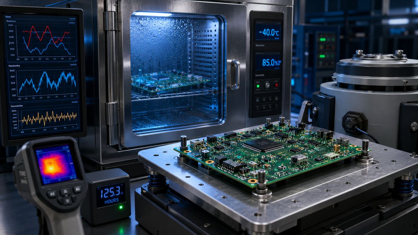
When Is PCB Reliability or Environmental Testing Required?
PCB environmental testing examines whether the board, materials, interconnections, and assembly process can survive expected service conditions.
It may be required when:
- The product operates at high or low temperature
- Temperature changes are frequent
- The assembly experiences vibration or shock
- Humidity or condensation is possible
- High current flows through vias or plated holes
- The board contains HDI microvias
- Field access is difficult
- Failure creates safety or financial risk
- A customer or regulatory plan specifies qualification tests
Interconnect Stress Testing
IST evaluates the durability of plated through-holes, vias, and other interconnect structures by cycling the test coupon through controlled heating and cooling.
The method uses DC current to resistance-heat the interconnect structure, creating repeated thermal excursions and thermo-mechanical fatigue.
IST is especially useful when assessing multilayer constructions, plated-hole quality, HDI structures, or process changes.
Thermal Cycling and Thermal Shock
Thermal cycling gradually moves the sample between temperature extremes. Thermal shock uses more abrupt transitions.
These tests can expose:
- Barrel cracking
- Pad lifting
- Microvia separation
- Laminate stress
- Solder fatigue
- Component and PCB expansion mismatch
Test temperature, dwell time, ramp rate, cycle count, sample size, and failure criteria should come from the product qualification plan.
Temperature and Humidity Testing
Humidity testing evaluates insulation, corrosion resistance, contamination, and moisture-related degradation.
It may be combined with electrical bias when the objective is to study leakage paths, electrochemical migration, or insulation resistance.
Vibration and Mechanical Shock
Vibration and shock testing are relevant to vehicles, industrial machinery, aircraft, handheld equipment, and products shipped in demanding conditions.
The test fixture should reproduce the intended mounting points. Supporting the sample incorrectly may create a failure mode that would not occur in the actual enclosure.
CAF and SIR Testing
Conductive anodic filament testing evaluates electrochemical growth through laminate material between conductors.
Surface insulation resistance testing evaluates electrical resistance across a contaminated or moisture-exposed surface.
These methods are normally used for material, process, cleanliness, or reliability qualification rather than routine PCB board testing.
Third-Party PCB Testing Laboratories
A third-party laboratory may be appropriate when the project requires:
- Independent qualification
- Specialized environmental chambers
- Failure analysis
- Microsection evaluation
- Ionic contamination testing
- Material verification
- Regulatory documentation
- Customer-witnessed testing
Before ordering laboratory work, define the test method, sample condition, preparation method, acceptance limit, reporting format, and handling of failed samples.
What Should Be Included in a PCB Testing Report?
A useful PCB testing report must connect the result to the correct product, revision, process, and test program.
It should include:
- Customer or project name
- PCB or PCBA part number
- Board revision
- Manufacturing lot
- Serial number, where applicable
- Test date and time
- Test-station identification
- Fixture revision
- Software or program revision
- Firmware version
- Test method
- Measured values
- Upper and lower limits
- Pass/fail result
- Failed net, component, or test step
- Operator or system identification
- Retest status
- Repair or rework record
For prototype debugging, waveform captures, X-ray images, AOI defect images, and failed measurements can be more useful than a simple pass/fail certificate.
The report format should be agreed before production. Reconstructing missing traceability after shipment is far harder than recording it during the test.
How Does EBest Circuit Test PCB and PCBA Orders?
EBest Circuit builds the test plan around the manufacturing stage, product complexity, production quantity, and customer requirements.
Available quality-control and testing support can include:
- Bare-board electrical testing
- Solder paste inspection
- Automated optical inspection
- X-ray inspection
- Flying probe testing
- ICT fixture coordination
- Firmware programming
- Functional test jig development
- Functional circuit testing
- Test-report preparation
- MES and lot traceability
- Reliability testing based on project requirements
For PCBA functional testing, customers should provide the schematic, product specification, firmware, interface definitions, expected measurements, pass/fail limits, and a working golden sample where available.
Providing this information during quotation allows the engineering team to evaluate fixture cost, test coverage, cycle time, programming needs, and equipment requirements before production begins.
For PCB fabrication, turnkey PCBA, or a project-specific PCB testing procedure, contact sales@bestpcbs.com for a DFM and testability review.
Frequently Asked Questions About PCB Testing
1. What is the most common PCB testing method?
For bare PCBs, electrical continuity and isolation testing are common production checks. For assembled PCBAs, AOI is widely used after reflow, often combined with X-ray, flying probe, ICT, or functional testing depending on the board.
There is no single test that covers every defect.
2. What is the difference between PCB testing and PCBA testing?
PCB testing normally refers to an unpopulated board and focuses on copper connections, opens, shorts, and isolation.
PCBA testing is performed after components are installed. It may check soldering, component values, firmware, power rails, interfaces, and complete circuit operation.
3. Is flying probe testing better than ICT for prototypes?
Flying probe is usually more practical for prototypes because it does not require an expensive dedicated bed-of-nails fixture and can accommodate design revisions more easily.
ICT becomes more attractive when the design is stable and production volume is high enough to justify fixture development.
4. Can AOI detect electrical faults on a PCB?
AOI can detect many visible assembly defects, such as missing components, polarity errors, shifted parts, and some solder problems.
It cannot directly prove continuity, component value, firmware operation, or circuit function. Electrical testing is still needed for those checks.
5. What does a PCB functional test check?
A PCB functional test powers the assembly and checks whether it operates according to the product specification.
It may measure current, voltages, signals, communications, sensors, outputs, displays, switches, relays, or protection functions.
6. Does every PCB need environmental reliability testing?
No. Routine commercial boards may not need full thermal, humidity, vibration, or burn-in qualification.
These tests are more relevant when required by the application, customer specification, qualification plan, safety risk, or expected operating environment.
7. What files are required to develop a PCB testing jig?
The exact package depends on the test, but it often includes:
- Gerber or ODB++ files
- Schematic
- BOM
- Pick-and-place data
- Test-point list
- Mechanical drawing
- Connector definition
- Firmware
- Programming instructions
- Functional test procedure
- Expected limits
- Golden sample
Complete and revision-controlled data reduces fixture rework and improves test coverage.
Ready to Define the Right PCB Testing Plan?
Match the test strategy to the board stage, product risk, production volume, and required fault coverage. For a project-specific review, send EBest Circuit the Gerber data, BOM, schematic, quantities, test limits, firmware, and available golden sample.