





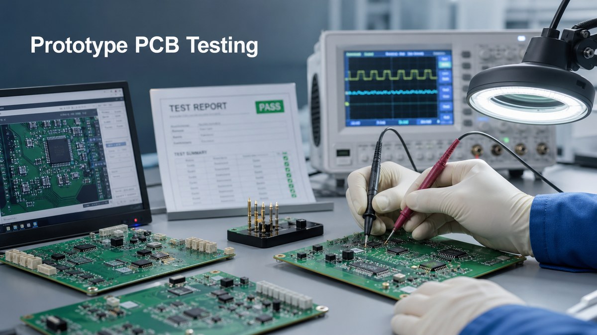
The best way to test prototype PCBs is to build a clear validation plan before production starts. A prototype is not only a sample board. It is the first proof that the files, stackup, components, assembly process, soldering quality, and product function are ready for the next build.
Prototype failure is expensive because the real cost is often time. A board that cannot be validated may delay firmware debugging, enclosure fitting, certification planning, pilot production, and customer delivery. EBest Circuit (Best Technology) supports PCB prototype board and PCBA projects with DFM review, PCB fabrication, component sourcing, SMT assembly, inspection, testing coordination, and engineering feedback. If you are preparing a turnkey prototype assembly project, send your Gerber files, BOM, stackup, assembly files, drawings, and test notes to sales@bestpcbs.com for engineering review before production.
Best Way to Test Prototype PCBs Before Production
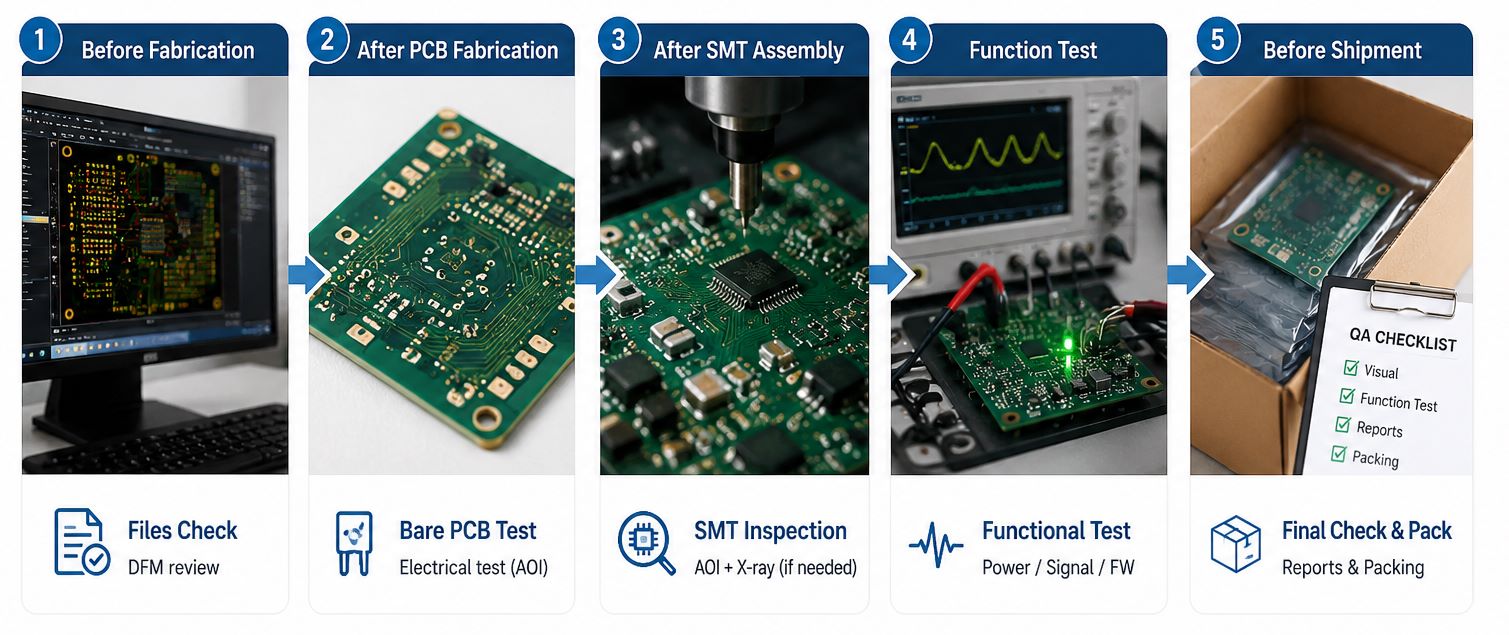
The best way to test prototype PCBs is to check them in stages. Each stage removes a different type of uncertainty before the project moves forward.
| Stage | What It Confirms | Risk If Skipped |
|---|---|---|
| Before fabrication | Files are manufacturable | Build delay or EQ after order release |
| After PCB fabrication | Copper network is correct | SMT cost added to a defective bare board |
| After SMT assembly | Parts and solder joints are acceptable | Prototype fails during bring-up |
| Before shipment | Required test and packing notes are complete | Board arrives but cannot be validated |
A prototype test plan should not be vague. It should define:
- which checks are done by the PCB factory
- which checks are done after SMT assembly
- which product-level tests require customer firmware or test fixtures
- which reports are required before shipment
- which findings should be fed back before the next build
Different defects appear at different stages. A bare PCB may pass electrical testing but still fail after assembly if a connector footprint is wrong. A PCBA may pass visual inspection but fail because one voltage rail is unstable. A BGA assembly may require X-ray because the solder joints are hidden under the package.
Prototype PCB Testing Checklist for First Build Validation
A strong prototype PCB testing checklist starts with the production files. The first build should answer a practical question: can this board be fabricated, assembled, inspected, and tested without unclear handoffs?
Files to prepare before quotation or production:
- Gerber or ODB++ data
- Drill files
- Stackup or board thickness notes
- Fabrication drawing
- BOM
- Pick-and-place file
- Assembly drawing
- Polarity notes
- Impedance requirements
- Test instructions
Items EBest Circuit reviews before production:
| Item | What Should Be Confirmed |
|---|---|
| Stackup | Board thickness, copper weight, impedance needs |
| Drill file | PTH, NPTH, vias, slots, and tolerances |
| BOM | Part availability and package match |
| Polarity | Diodes, ICs, LEDs, capacitors, connectors |
| Test notes | Firmware, test jig, test points, pass/fail criteria |
Confirming these items before production helps reduce rework, waiting time, and failed prototype validation.
Electrical Testing for Bare Prototype PCBs
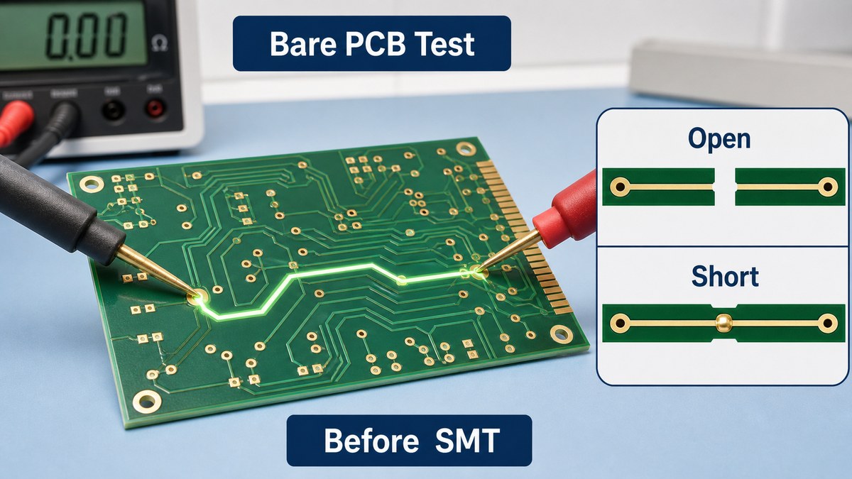
For bare prototype PCBs, electrical testing checks the copper network before components are assembled. It is the first safety gate before SMT cost is added.
Electrical testing can help find:
- open circuits
- short circuits
- wrong net connections
- netlist mismatch
- plating-related connection problems
- process defects that may not be obvious visually
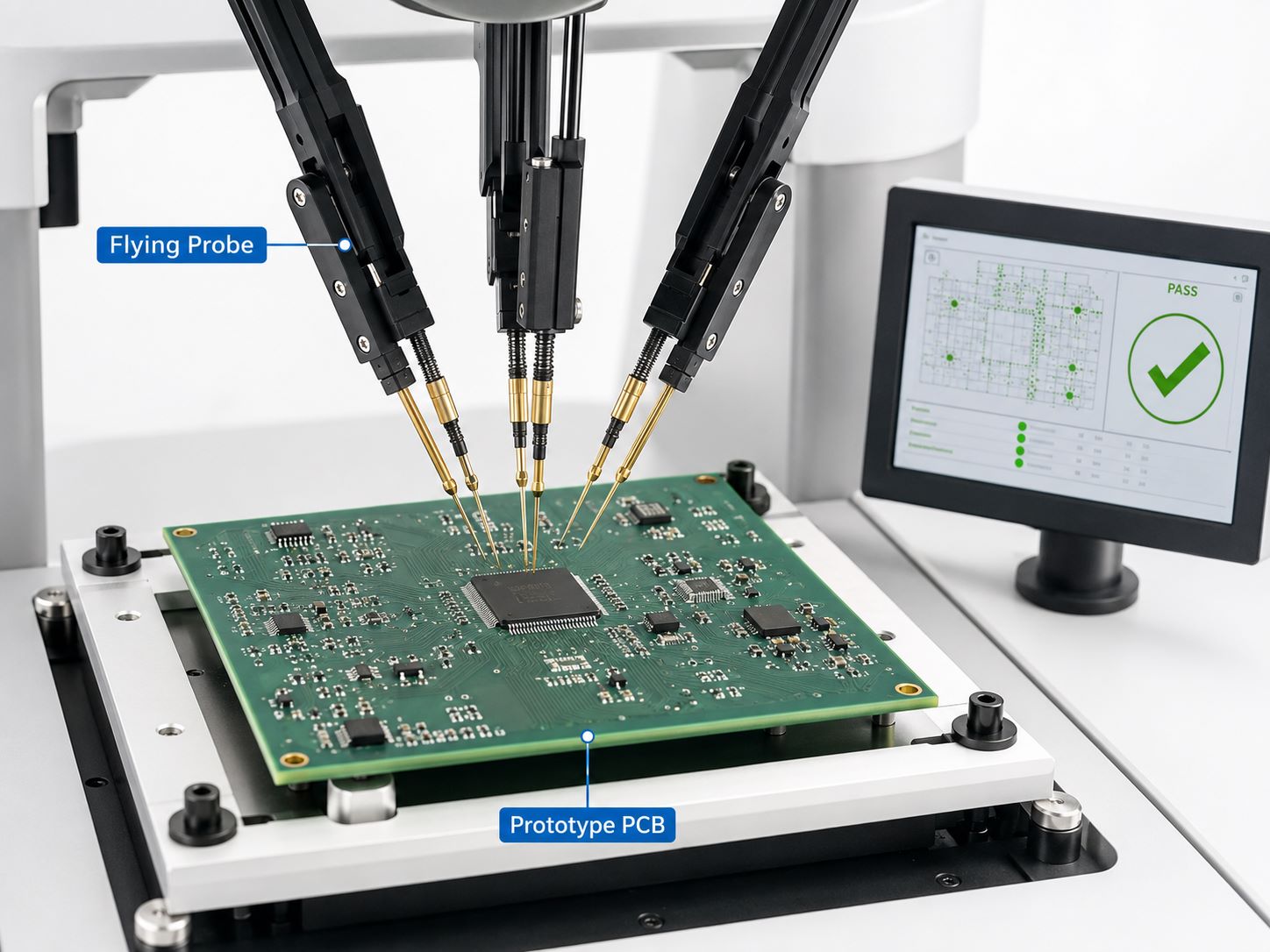
For prototype and small-to-medium volume boards, EBest Circuit can use flying probe testing to check open and short circuits. For medium and large volume production, universal electrical testing or fixture-based testing may be more suitable.
A prototype PCB should not move to assembly only because it “looks fine.” The copper network should be verified first.
Flying Probe Testing for Prototype PCB Fabrication
Flying probe testing is often suitable for prototype PCB fabrication because it does not require a custom test fixture. This is useful when the design may still change after the first build.
| Situation | Why Flying Probe Fits |
|---|---|
| First prototype | No fixture cost before design is stable |
| Small quantity | Suitable for low-volume validation |
| Possible engineering change | Easier than rebuilding a fixture |
| Netlist verification | Helps find opens and shorts |
Flying probe testing is especially useful when the customer needs a quick validation batch but does not want to invest in a test fixture too early. If the design later moves into repeat production, fixture-based testing can be reviewed.
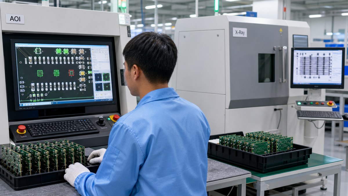
AOI and X-Ray Checks After SMT Assembly
After SMT assembly, the main risk is no longer only the PCB copper network. The assembled board may fail because of soldering, placement, polarity, or hidden joint issues.
EBest Circuit’s SMT inspection flow may include:
- incoming PCB and component review
- baking when needed
- solder paste printing
- SPI before placement
- component placement
- reflow soldering
- post-reflow inspection
- AOI
- X-ray when BGA or hidden joints require it
- cleaning
- programming or testing
- final packing
SPI checks before placement:
- solder paste volume
- solder paste area
- solder paste height
- solder paste thickness
- offset
- bridging
- insufficient paste
AOI checks after reflow:
- missing parts
- wrong parts
- polarity errors
- rotation
- tombstoning
- bridging
- insufficient solder
- lifted leads
- visible solder defects
X-ray checks hidden joints:
- BGA solder joints
- voids
- hidden solder bridges
- wetting issues under packages
These inspection points catch different defects before they accumulate at final testing.
Functional Test for Prototype PCB Assembly
A functional test checks whether the assembled PCBA works in the intended application. It is different from bare board electrical testing.
Functional testing depends heavily on customer-provided information. Before production, the test scope should be clear.
The customer should provide:
- test instructions
- firmware or programming files
- test points
- expected voltage or current values
- interface requirements
- pass/fail criteria
- test jig or fixture requirements, if needed
Functional testing may check:
| Test Area | Example |
|---|---|
| Power-up | Startup behavior and current draw |
| Voltage rails | 3.3V, 5V, or other required rails |
| Communication | USB, UART, CAN, Ethernet, wireless interface |
| Programming | MCU, memory, or IC programming |
| Customer fixture | Product-specific validation |
When the test method is clear, EBest Circuit can coordinate functional testing as part of PCBA manufacturing. This is useful when a project needs PCB fabrication, component sourcing, SMT assembly, inspection, and test communication under one workflow.
Power, Signal, and Connector Checks on Prototype PCBs
Many prototype failures appear around power, signal, and connector areas. These areas should be reviewed early because they often affect bring-up, debugging, and enclosure validation.
Power checks should review:
- startup behavior
- voltage rails
- current draw
- regulator heating
- high-current paths
- thermal vias or copper area where needed
Signal checks may involve:
- impedance
- differential pairs
- return paths
- grounding
- clock lines
- connector routing
- high-speed or RF-sensitive paths
Connector checks should confirm:
- footprint match
- orientation
- board edge clearance
- insertion direction
- mechanical fit
- solder joint strength
A board can be manufacturable but still difficult to assemble, test, or validate. Early DFM and assembly review help find these issues before they become production delays.
How EBest Circuit Controls Prototype PCB Quality During Manufacturing
EBest Circuit controls prototype PCB quality through staged checks instead of relying only on final inspection.
| Stage | Control Point |
|---|---|
| Before production | DFM review, EQ questions, file confirmation |
| PCB fabrication | Stackup, drilling, plating, AOI, surface finish |
| Bare board | Flying probe or electrical testing |
| SMT preparation | BOM check, incoming inspection, baking when needed |
| SMT process | Solder paste printing, SPI, placement, reflow |
| After reflow | AOI, X-ray when needed, manual inspection |
| Final stage | Cleaning, programming/test, packing, reports if required |
PCB inspection and measurement support may include:
- flying probe testing
- universal electrical testing
- AOI
- impedance testing
- copper thickness testing
- 3D measurement
- V-cut depth testing
- hole diameter testing
- micro-section analysis
PCBA process control may include:
- SMT stencil printing
- 3D SPI
- Yamaha placement
- nitrogen reflow
- 3D AOI
- X-ray inspection
- functional testing
- cleaning
- final inspection
Prototype PCB quality is checked through the production path, not only at the shipping stage.
Prototype PCB Testing Case Study at EBest Circuit
A customer needed prototype PCBA for an electronic control product. The project looked straightforward, but it required careful coordination between PCB fabrication, BOM sourcing, SMT assembly, inspection, and final delivery.
Project details:
- 4-layer FR4 PCB
- Tg130 material
- 1.6mm finished thickness, +/-10%
- 1oz copper on each layer
- Black solder mask, white silkscreen
- Lead-free HASL
- Free panelization for fabrication
- Components sourced by EBest Circuit
- SMT assembly
- Individual delivery after SMT
Main project risk: handoff
If PCB fabrication, component sourcing, SMT, and inspection were managed by separate suppliers, small build notes could be missed. For a prototype, those missed notes may delay bring-up or make the first build harder to evaluate.
EBest Circuit’s workflow:
- reviewed the production files
- confirmed the build requirements
- arranged PCB fabrication
- sourced the components
- completed SMT assembly
- inspected boards after reflow
- packed assembled units individually
The same team kept the project notes visible from file review to final packing. This workflow made the first build easier to evaluate and helped the customer decide whether the project was ready for the next validation batch.
Why Choose EBest Circuit for Prototype PCB and PCBA Manufacturing?
EBest Circuit is a good fit when a prototype project needs more than bare PCB fabrication. For engineering teams, the value is in one coordinated workflow: PCB fabrication, component sourcing, SMT assembly, inspection, testing support, and production feedback.
What EBest Circuit helps control:
- File and DFM risk
Gerber files, stackup, drill data, panelization, BOM, polarity marks, assembly notes, and test requirements can be reviewed before production. - PCB manufacturing risk
EBest Circuit supports FR4 PCB, HDI PCB, flex PCB, rigid-flex PCB, ceramic PCB, metal core PCB, high Tg PCB, heavy copper PCB, and impedance-controlled PCB manufacturing. - Component and assembly risk
The team can coordinate component sourcing, SMT assembly, AOI, X-ray when required, functional test coordination, cleaning, packing, and production notes. - Quality and traceability risk
EBest Circuit holds ISO9001, ISO13485, IATF16949, AS9100D, REACH, RoHS, and UL-related quality support, with process control and production traceability. - Prototype-to-small-batch risk
After the first build, production feedback can help engineers decide whether the project is ready for another prototype, a small batch, or design adjustment.
This makes EBest Circuit suitable for prototype PCB and PCBA projects, from an early proto board build to a small validation batch, where technical details must stay visible from file review to final delivery.
FAQs about Testing Prototype PCBs
1. What is the best way to test prototype PCBs?
The best way is to combine DFM review, bare board electrical testing, SMT inspection, AOI, X-ray when needed, functional testing, and engineering feedback before scaling production.
2. Is flying probe testing enough for prototype PCBs?
Flying probe testing helps check opens and shorts on prototype PCBs. It does not replace SMT inspection or functional testing after assembly.
3. Do prototype PCB assemblies always need functional testing?
Not always. If product-level validation is required, functional testing should be defined. The customer should provide firmware, test method, and pass/fail criteria.
4. When is X-ray needed for prototype PCB assembly?
X-ray is usually needed for BGA, QFN, LGA, or other hidden solder joints. If all solder joints are visible, AOI and manual inspection may be enough.
5. What should I send before prototype PCB production?
Send Gerber or ODB++ files, drill files, stackup, BOM, pick-and-place file, assembly drawing, test notes, firmware if needed, and any special inspection or packing requirements.
In closing, if you are not sure which tests your prototype PCB or PCBA needs, please send your Gerber files, BOM, stackup, assembly files, and test notes to sales@bestpcbs.com. EBest Circuit’s engineering team can review the manufacturing and testing path before production starts.
You may also like

Tags: best way to test prototype pcbs, prototype pcb test, prototype PCB testing