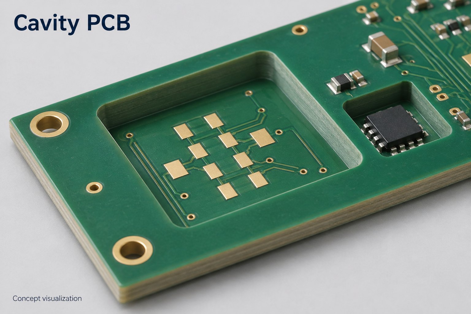
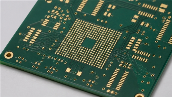
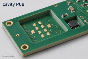
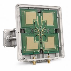
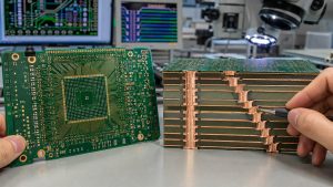
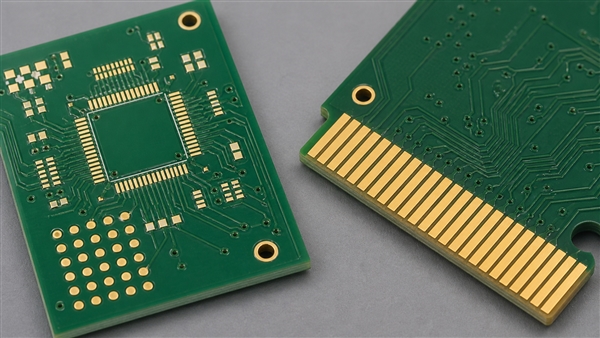
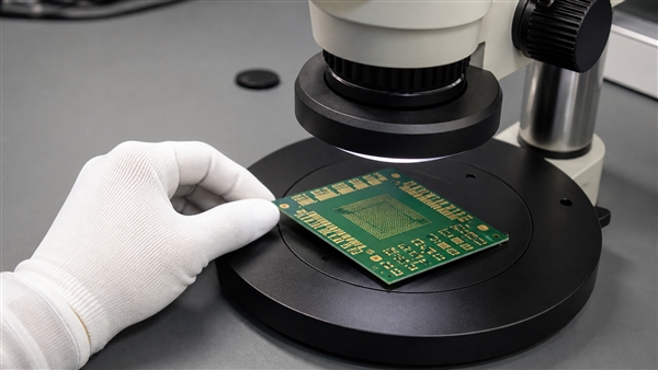
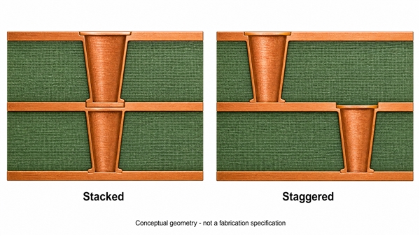
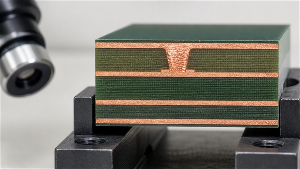
A cavity PCB provides a lower mounting surface for components within part of the board. It can help a tall package fit beneath an enclosure cover while leaving the surrounding board at its original thickness. The recess also changes where component pads sit, which copper layers remain available and how the assembly equipment reaches the footprint.
EBest Circuit provides multilayer PCB fabrication, DFM support, component sourcing and PCB assembly. For a recessed-component project, a combined fabrication and assembly review can address the cavity geometry alongside the mounting process. Contact sales@bestpcbs.com to discuss your board stackup and component arrangement.
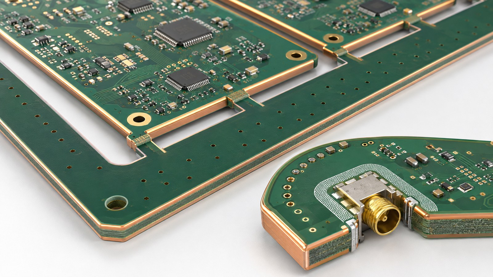
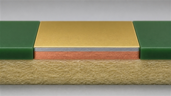
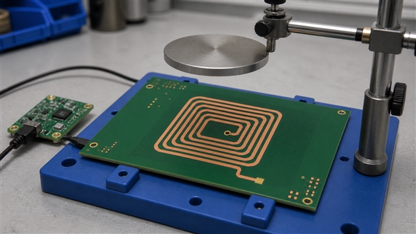
Concept visualization of a cavity PCB with recessed mounting areas.
What Is a Cavity PCB?
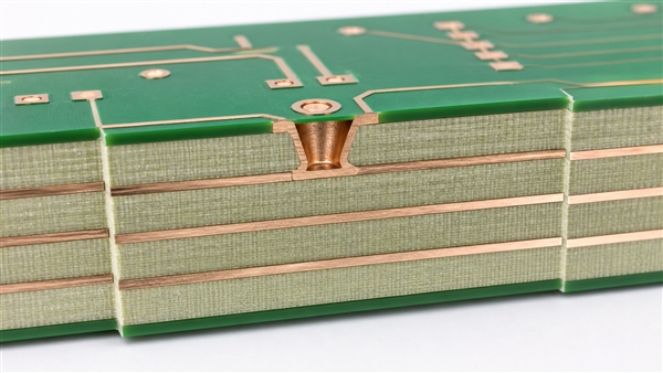
A cavity is a local recess with a floor and board material beneath it. Depending on its construction, that floor can be bare dielectric, a copper surface or a circuit layer containing pads and traces.
Feature
Cross-section
Typical use
PCB cavity
A recess that stops within the board thickness
Mount a component below the outer surface or expose an internal layer
Through-cutout
An opening through the full board thickness
Provide clearance through the board
Counterbore
A larger cylindrical recess around a smaller hole
Seat a screw head or washer below the surface
For an SMD component mounted on the cavity floor, the exposed layer contains its footprint. The board must therefore preserve both the recessed shape and the copper features that connect the component to the circuit.
How Do Recessed Components Reduce Assembly Height?
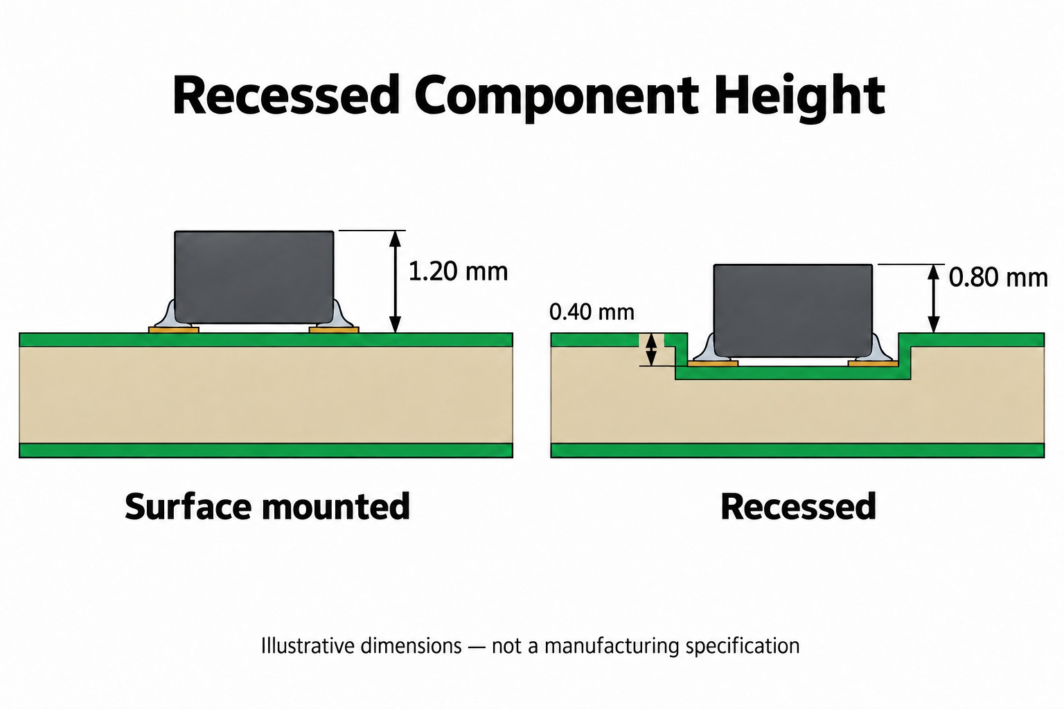
The height saved above the board comes from lowering the component’s mounting plane. The package itself stays the same size.
Here, assembled component height means the distance from the mounting-pad surface to the top of the installed component, including its soldered standoff. Cavity depth is measured from the surrounding board surface to that lower pad surface.
Component-top position relative to the board surface = assembled component height − cavity depth
For example, an assembled height of 1.20 mm and a recess depth of 0.40 mm leave the component top 0.80 mm above the board. A negative result would place it below the surrounding surface.
For the largest possible protrusion, use the maximum assembled height and the minimum recess depth. That upper position is what must fit beneath the enclosure cover, with the intended gap remaining.
This geometric example does not imply a manufacturing tolerance. Recessing one package also cannot reduce the enclosure height if a taller connector elsewhere still sets the limit. Increasing the board thickness to make room for the cavity can offset the height saved above it.
Lowering the mounting plane reduces component protrusion. Dimensions are illustrative.
How Do Copper Floors and Plated Walls Change a PCB Cavity?
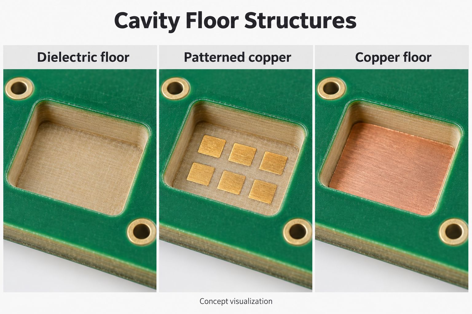
A bare pocket, a recessed footprint and a metal-lined cavity have different electrical structures. The distinction is where the copper remains and what it connects to.
Copper arrangement
Structure inside the cavity
No exposed copper
The floor is dielectric, with no conductive landing area for a soldered connection.
Patterned floor
Separate pads and traces form a component footprint or bonding pattern. Gaps between the copper features separate different electrical nets.
Continuous copper floor
A single conductive area can connect to ground or form part of a heat-spreading structure.
Plated walls
Metal extends along the sides of the recess and can connect to designated copper layers, such as ground.
A patterned floor can coexist with plated walls. In that arrangement, signal pads remain separated from grounded wall metal; otherwise, the plating could join conductors that should be isolated. Floor pattern and wall plating therefore need separate definitions in the cavity design.
Concept comparison of dielectric, patterned-copper and continuous-copper cavity floors.
How Are PCB Cavities Manufactured?
Manufacturers form cavities through controlled-depth machining, lamination-based construction, laser processing or a combination of these methods.
Controlled-depth routing: A cutter removes material to a set depth. It leaves rounded internal corners and a machined floor. This process must stop before removing any copper or dielectric intended to remain below the pocket.
Lamination-based construction: Openings can be built into selected layers, with resin flow controlled around the cavity. Another approach forms a removable cap above a prepared inner layer; removing the cap exposes the recessed circuit pattern.
Laser processing: Laser energy removes dielectric to expose a metal surface or patterned circuitry. Near a patterned layer, controlled passes remove the remaining resin around copper features. Wall taper and floor cleanliness depend on the material and laser process.
For some constructions, routing removes most of the material and laser processing finishes the region near the target layer. This combines bulk removal with more selective exposure of the cavity floor.
What Limits Cavity PCB Design?
The main constraints are the material left beneath the cavity, the copper it approaches and the space needed around the component.
A deeper cavity leaves a thinner floor: For a simple one-sided pocket, minimum remaining thickness equals minimum board thickness minus maximum cavity depth. The remaining section must still contain the intended dielectric and circuitry. Increasing depth can remove that insulation or intersect an internal conductor.
A fixed depth is different from exposing a copper layer: A pocket dimensioned from the top surface is controlled by that surface reference. A cavity intended to expose an inner pad layer must also follow the layer’s actual position in the stackup. A nominal depth alone does not describe how to uncover the pads while preserving them.
Rounded corners can interfere with a square package: A routed pocket may match the package’s width and length along its straight sides yet still obstruct its corners. The cutter radius leaves material in those corners, so the package outline and cavity outline must be compared together.
Copper clearance extends beyond the visible opening: Traces, planes and vias on affected layers need separation from the finished wall and the possible machining variation. Moving surface copper alone does not protect a conductor buried beside the recess.
Package fit does not establish placement access: An opening that admits the component body may still obstruct the placement nozzle. Clearance must accommodate the tool as it lowers the package onto the recessed pads.
How Does Cavity Depth Affect SMT Assembly?
Cavity depth changes the vertical relationship between the stencil, pads and placement tool. The assembly process must reach the recessed footprint without being obstructed by the surrounding board.
Printing on a lower surface: A flat stencil resting on the outer board surface can leave a gap above recessed pads. A cavity-matched step stencil brings the printing region down to the footprint; the squeegee arrangement must also follow the stencil’s contour.
Placing at the recessed height: The placement machine must seat the component at the lower pad level. The nozzle’s shape and approach need enough clearance to avoid the walls during that movement.
In an AT&S cavity-assembly study, a step stencil and customized squeegee enabled printing, while paste-volume process capability decreased across the deeper test configurations. Placement and reflow were successful in that trial. The result shows that workable assembly and unchanged printing consistency are different claims; it does not establish a universal depth limit.
Can PCB Cavities Improve Cooling and RF Performance?
A cavity can shorten a heat path or change an RF structure, but those benefits come from specific connections and geometry.
Thermal path: Lowering a device can bring it closer to a conductive base or enclosure interface. Heat must still pass through the device attachment, intervening materials and the connection to the heat sink. An empty pocket supplies space; it does not supply that conductive path.
A buried copper coin PCB uses an inserted copper element to carry heat through part of the board. This is a different structure from leaving the recess open for a component.
RF structure: Replacing dielectric with an intentional air region changes the electrical environment around a signal or antenna. Grounded metal walls can also contribute to isolation. The resulting impedance and resonances depend on dimensions, dielectric distribution and ground connections, so an RF cavity belongs in the electromagnetic design.
Where shielding is the objective, an open metal-lined recess and a grounded enclosure with a lid have different boundaries. Sidewall plating alone should not be described as a complete shield.
Cavity PCB FAQs
Is a recessed component the same as a fully buried component?
No. A component in an open cavity can be reached from the open side. A fully buried component is enclosed within the board; reaching it would require opening or removing part of that structure.
Can cavities be made on both sides of a PCB?
Yes, in constructions that retain enough material between them. Where opposing pockets overlap, the remaining thickness is the local board thickness minus both recess depths. Their target copper layers must also remain intact.
Can one board contain cavities at different depths?
Yes. Separate cavities or stepped levels within a cavity can expose different layers. Each level has its own floor geometry; a footprint spanning two levels cannot be treated as a conventional flat mounting surface.
Can solder mask be applied inside a cavity?
Yes, some cavity processes support solder mask on a patterned floor. It can cover selected copper while leaving connection pads exposed. That floor coating is part of the fabrication sequence, rather than an automatic extension of the outer-surface mask.
Is a cavity outline in Gerber data enough to define the recess?
No. The outline defines its shape in the board plane, but not its vertical structure. A section view and fabrication notes identify the opening side, depth reference or target layer, remaining floor and any wall plating.
For your cavity PCB project, EBest Circuit can review the fabrication and PCBA requirements from your stackup, cavity section and component arrangement. Send these details to sales@bestpcbs.com to discuss the proposed build.
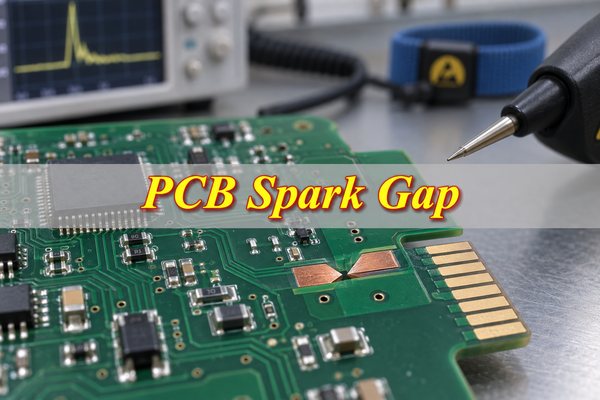
A PCB spark gap is a deliberate gap between exposed copper electrodes that gives ESD or another high-voltage transient a preferred place to discharge. It can divert current away from a sensitive signal or circuit, but it is not a precision clamp.
PCB spark gapdistance cannot be selected by simply dividing the ESD test voltage by 3 kV/mm. The voltage actually appearing across the electrodes, electrode geometry, altitude, contamination, solder mask, manufacturing tolerance, and discharge return all affect where the arc starts.
The practical task is to turn a first estimate into a gap that can be manufactured and tested. That means identifying the ESD entry and return, calculating a candidate range, dimensioning the finished copper, placing the diversion before the protected circuit, and releasing only the geometry that passes defined tests.
What Is a PCB Spark Gap and How Does It Work?
A PCB spark gap is an intentional air gap between two exposed copper electrodes. One electrode connects to the transient-exposed conductor; the other connects to a chosen discharge return, such as chassis or shield. When the electric field across the gap becomes high enough, the air ionizes and current jumps between the electrodes.
Gap distance sets only part of that behavior. Pointed copper concentrates the field, and the surrounding layout decides whether the resulting current follows the intended path. Because pressure, residue, geometry, polarity, and repeated arcing can shift the firing voltage, a PCB spark gap is a coarse diversion feature rather than a precision voltage clamp.
When the protected circuit needs tighter residual-voltage control, coordinate the gap with a TVS diode, GDT, or another protection stage instead of expecting the copper feature to act like a specified clamp.
What Does a PCB Spark Gap Protect Against?
A PCB spark gap is mainly used to divert ESD arriving through a known external interface. The most credible locations are connector pins, exposed contacts, cable entries, shield interfaces, and other points where the discharge can be intercepted before it crosses sensitive circuitry.
Connector-side ESD: The gap offers an early diversion point before the pulse travels along a signal or control trace.
Exposed interfaces: It can steer a discharge away from component leads, test points, and narrow internal clearances.
Cable or chassis entry: A short gap-to-chassis path can keep high-frequency current near the product boundary.
Secondary diversion: It can provide a coarse backup path when another stage limits current or residual voltage.
A bare PCB gap is not a reliable substitute for a rated high-energy surge device. It is also a poor fit when the protected node needs a narrow clamping range. An intentional firing gap does not replace required creepage, clearance, or safety insulation. Its value comes from making one discharge path preferable to the alternatives. A gap that fires into a long or sensitive return can still leave damaging voltage across the circuit.
What Electrical and Environmental Factors Affect PCB Spark Gap Distance?
Six factors determine how a first estimate becomes a testable PCB gap. Each one changes either the electrical stress, the local field, or the finished geometry. The right response is not another generic formula; it is a specific design or validation action.
Design Factor
Effect on Breakdown Voltage
Practical Consideration
Actual voltage across the gap
Sets the electrical stress that the electrodes must withstand or discharge.
Model or measure Vgap; do not substitute the generator setting.
Electrode geometry
Sharp features intensify the local electric field.
Freeze shape, orientation, and finished tip radius before comparing gaps.
Pressure and altitude
Change gas density and the pressure-distance relationship.
Do not reuse sea-level validation for a higher-altitude requirement.
Surface contamination
Can promote leakage, surface tracking, or a carbonized path.
Set cleanliness limits and inspect after repeated events.
Mask and coating
Change or redirect the exposed discharge path.
Dimension keepouts and control later coating operations.
Fabrication tolerance
Changes the actual distance and edge profile.
Measure production-intent boards and test the finished distribution.
How Do You Calculate PCB Spark Gap Distance?
Calculate a candidate gap, then prove it on finished hardware. A useful first-order estimate divides the voltage expected across the gap by an assumed air-breakdown field:
Estimated gap distance: dest = Vgap / Eassumed
For example, if the protection network is estimated to place 3 kV across the electrodes and the first pass uses 3 kV/mm, the arithmetic gives an estimated distance of 1.0 mm. That does not mean a 1.0 mm PCB gap will reliably fire at exactly 3 kV. Pointed electrodes create a nonuniform field, and the board surface introduces other possible paths.
Step 1: Establish Vgap. Characterize the ESD source, polarity, rise time, and source impedance. Then account for every element between the entry point and return. A TVS diode, GDT, series impedance, or parasitic coupling can change how much of the generator voltage appears between the spark-gap electrodes.
Step 2: Calculate the first-order distance. Apply dest = Vgap / Eassumed with the pressure, gas, field, and waveform assumptions written beside the result. Using 3 kV/mm may be acceptable for an order-of-magnitude check, but not for setting a production tolerance.
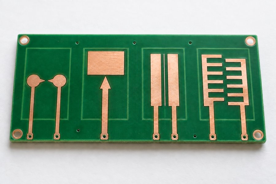
Step 3: Adjust for electrode geometry. Decide whether the candidate uses point-to-point, point-to-plane, parallel-edge, or another controlled shape. The same minimum distance does not imply the same firing voltage because each geometry creates a different field distribution.
Step 4: Build a candidate range. Apply finished-copper and mask tolerances, then place several gaps around the estimate on a coupon or prototype. For an illustrative 1.0 mm estimate, the following set tests both earlier and later firing while holding geometry, finish, and return path constant.
Candidate
Finished Gap
Purpose
A
0.8 mm
Check earlier firing
B
1.0 mm
Test the initial estimate
C
1.2 mm
Check a higher threshold
D
1.4 mm
Probe the upper test range
Measure the finished gaps before testing. Use the same electrode shape, copper weight, surface finish, solder-mask opening, and return path planned for production.
For each candidate, record whether it fires at the target level, whether the arc stays between the intended electrodes, whether another feature flashes over first, and whether repeated events change the result. This comparison turns one uncertain calculation into evidence for selecting or rejecting a production geometry.
Paschen-type relationships can refine gas-breakdown estimates when pressure, distance, gas, and electrode conditions are defined. They still do not reproduce every feature of a PCB surface. The deliverable from calculation is therefore a documented prototype range with acceptance criteria, not a guaranteed firing voltage.
Can You Simply Use 3 kV/mm for PCB Spark Gap Calculation?
Use 3 kV/mm only for a rough first estimate under stated air and field assumptions. Pointed PCB electrodes, surface paths, pressure, contamination, and fast transient behavior prevent it from predicting a guaranteed production firing voltage.
Use
Suitable?
Rough first estimate
Yes, with assumptions recorded
Final production gap
No
Safety clearance
No
Guaranteed firing voltage
No
Compliance release
No
How Does Electrode Shape Affect PCB Spark Gap Distance?
Electrode shape determines where the electric field concentrates, how tightly the arc location is controlled, and how sensitive the feature is to fabrication. Two gaps that both measure 0.5 mm can behave differently when one uses sharp opposing points and the other uses broad parallel edges.
Geometry
Field Behavior
Manufacturing Sensitivity
When to Use
Point to point
Strong concentration at both tips
High; tip radius and erosion cause larger shifts
When a controlled arc location matters
Point to plane
Concentration at one tip
High at the pointed electrode
When a preferred initiation side is useful
Parallel edges
Field distributed along the edges
Moderate; edge width and etch still matter
When reproducibility matters more than one fixed arc point
Interdigitated teeth
Multiple local high-field regions
High; more edges collect process and contamination variation
Only when multiple initiation sites have been intentionally evaluated
Select the geometry according to the required arc control and production stability, not just the smallest CAD distance. Sharp tips can favor a specific discharge point, but their finished radius is highly process-sensitive. Broader edges can be easier to reproduce, while allowing the arc to move. Repeated events can erode either shape and carbonize the board surface, so the first firing result does not establish long-term behavior.
How Should You Design a PCB Trace Spark Gap?
Design the spark gap as a controlled layout object, not as two trace ends that happen to be close. The fabrication data must make six physical requirements unambiguous.
Finished copper-to-copper gap: Set the nominal value and allowed finished tolerance from the tested candidate range.
Electrode tip geometry: Use tips or edges the PCB process can reproduce, then dimension their finished relationship.
Copper width: Give the transient path enough width and keep the neck behind each electrode short.
Mask opening: Expose the active copper after allowing for solder-mask registration tolerance.
Surrounding clearance: Keep pads, vias, planes, board edges, and component terminals from becoming an easier arc path.
Discharge connection: Dimension enough copper behind the return electrode to avoid a narrow or inductive bottleneck.
Wrong layout logic: connector, then a long signal trace, then the spark gap. In this order, the ESD current has already traveled beside or through the protected circuit before reaching the diversion point.
Better layout logic: connector, then the spark gap, then the protected circuit. The gap intercepts the entry before the signal branches into the board, while its return electrode connects through a short, wide path to the chosen transient return.
Document the feature in the schematic, footprint, fabrication drawing, and assembly notes. This prevents automated copper cleanup, mask editing, or conformal coating from changing its function.
Where Should You Place a PCB Spark Gap for ESD Protection?
Place the spark gap as close as practical to the ESD entry point and before the transient reaches sensitive circuitry. Make the placement decision by answering three layout questions.
Where does ESD enter? Identify the connector pin, exposed metal, cable, switch, test point, or user-accessible contact that receives the event. Put the gap before that conductor reaches its first sensitive branch.
Where should the current leave? Select chassis, shield, or a dedicated transient return and verify continuity through connector shells, fasteners, seams, and return bonds. The gap should not discharge into an ordinary signal-ground path simply because it is nearby.
What must stay outside the path? Keep clocks, reset lines, analog inputs, high-impedance nodes, communication traces, and their reference copper away from both the arc site and the return route. Inspect every layer for coupling into planes or traces below the feature.
Texas Instruments shows a 0.2 mm connector-side pattern in one battery-gauge application. That is useful evidence that etched gaps can be integrated near an interface, but 0.2 mm is not a universal PCB spark gap distance. The referenced circuit, environment, geometry, current return, and validation target must be comparable before any pattern is reused.
How Do PCB Manufacturing Tolerances Affect the Final Gap Distance?
The CAD gap is not the finished gap, and minimum trace/space capability does not guarantee repeatable spark-gap geometry. Etching changes the copper edges, an ideal point becomes a finished radius, and mask registration changes the exposed path. Convert those effects into explicit order requirements.
The fabrication drawing should state:
Nominal finished gap measured copper to copper, not only the CAD distance.
Allowed gap tolerance and the sampling or inspection method used to verify it.
Electrode geometry including the dimensioned tip or facing-edge profile.
Solder-mask opening with registration allowance around the active electrodes.
Copper weight used by the tested design because etching behavior changes with copper thickness.
Surface finish matching the electrically validated samples.
Conformal-coating keepout when the design depends on an exposed-air path.
Inspection requirement covering the finished gap, electrode profile, mask opening, and keepout.
Intentional-feature note so CAM review does not close, widen, or remove the unusual spacing.
For a manufacturing review, also provide the Gerber or ODB++ files and the target ESD or functional requirement. Ask the PCB manufacturer to confirm which dimensions can be controlled and measured as finished features. Then measure boards from production-intent panels before electrical testing. Release criteria should cover the resulting distribution, not one ideal coupon.
When Should You Combine a PCB Spark Gap With a TVS Diode or GDT?
Add a TVS diode or GDT when the PCB spark gap alone cannot hold the protected node within its voltage limit, absorb the required energy, or survive the expected number of events. Device choice starts with clamping accuracy, event energy, repetition, capacitance, and the maximum voltage the downstream circuit can tolerate.
The roles are distinct: the PCB spark gap provides coarse diversion, a TVS controls residual voltage more tightly, a GDT handles higher-energy diversion, and series impedance coordinates current between stages. One possible sequence places the connector first, followed by a PCB spark gap or GDT, series impedance, a TVS diode, and the protected IC. Verify the turn-on order, protected-node voltage, current sharing, component stress, and function after repeated events.
How Should You Validate a PCB Spark Gap Before Production?
Validate the finished board under a defined equipment-level test and inspect both electrical behavior and physical damage. IEC 61000-4-2 establishes a common basis for equipment ESD immunity testing, but the applicable severity and acceptance criteria still come from the product requirement.
Step 1: Measure. Record the finished gap, tip profile, mask opening, finish, and residue condition on production-intent samples.
Step 2: Test. Apply the defined ESD method, levels, polarities, points, operating states, and pulse count at relevant environmental corners.
Step 3: Observe the discharge path. Confirm that the intended gap fires before a component lead, connector edge, enclosure seam, or unrelated copper feature.
Step 4: Monitor the circuit. Capture protected-node voltage and record resets, corruption, latch-up, communication errors, damage, and recovery.
Step 5: Inspect repeated-event damage. Look for tip erosion, carbon tracks, coating damage, firing drift, and accumulated functional degradation before making the release decision.
A candidate passes only when:
the intended gap fires before another PCB or enclosure feature;
no unintended flashover occurs;
the protected circuit remains functional during and after the required test;
the measured transient at the protected node stays within the circuit’s accepted limit;
repeated pulses do not create progressive carbon tracking or unacceptable firing drift; and
production-intent boards show consistent behavior across the allowed finished-gap range.
Keep the release record tied to board revision, fabrication lot, measured geometry, firmware state, test setup, and acceptance limits. A visible spark alone is not a pass.
What Common PCB Spark Gap Design Mistakes Should You Avoid?
Most failures come from treating the gap as an isolated CAD dimension instead of a manufactured discharge path. These six checks catch the highest-value errors before compliance testing.
Copying a published gap value: The same distance can fire differently when electrode shape, finish, altitude, return path, or test setup changes.
Using the ESD generator setting as Vgap: Other protection elements and coupling paths can change the voltage that appears across the electrodes.
Putting the gap after a long signal trace: ESD current has already entered the circuit before it reaches the diversion point.
Leaving an easier unintended path: A nearby pad, via, plane, connector shell, component lead, or board edge may flash over first.
Using a poor return path: Shared return impedance can raise the local reference voltage even when the intended gap fires.
Treating the gap as safety clearance: A spark gap is intended to break down, while safety spacing is intended to prevent breakdown.
FAQs About PCB Spark Gaps
Q1: Can a PCB spark gap protect USB, CAN, or RS-485 interfaces?
A1: It can provide coarse diversion at the connector, but it is usually only one part of the protection network. A suitable TVS diode may still be needed to control residual voltage. For high-speed interfaces, verify the protection network’s capacitance, signal integrity, protected-node voltage, and recovery after repeated ESD events.
Q2: Why does a PCB spark gap sometimes fail to fire during ESD testing?
A2: Check the finished gap first, then confirm that enough transient voltage actually appears across the electrodes. Rounded tips, solder mask, coating, pressure, surface condition, or another protection device can change the discharge path. Measure the waveform and inspect the exposed geometry before reducing the distance.
Q3: Can you simulate a PCB spark gap before building the PCB?
A3: Field simulation can compare electrode shapes and electric-field concentration, while circuit simulation can examine voltage division and protection coordination. Neither method fully predicts statistical air breakdown, contamination, tip erosion, or finished-board tolerance. Use simulation to narrow the candidate range, then establish release values on measured hardware.
Q4: Does copper weight affect PCB spark gap performance?
A4: Yes. Copper thickness affects etching and can change the finished tip profile, edge shape, and copper-to-copper distance. If copper weight changes between prototype and production, ask the manufacturer to confirm the new finished geometry and repeat the relevant electrical tests before treating the earlier result as valid.
Q5: Should a PCB spark gap use ENIG, HASL, or another surface finish?
A5: No single finish is automatically best for every spark gap. The finish can alter the exposed surface, edge profile, oxidation behavior, and local repeatability. Keep the production finish consistent with the tested samples, or requalify the gap when a process change alters the finished electrodes.
Q6: Can a PCB spark gap be placed on an inner PCB layer?
A6: Not when the intended mechanism is an exposed-air discharge. An inner-layer gap is surrounded by solid dielectric and behaves differently from an external exposed structure. Keep a conventional PCB spark gap on an exposed surface unless a separately engineered internal structure has its own electrical and reliability validation.
Q7: Can multiple PCB spark gaps be used on one connector?
A7: Yes, when several exposed conductors can receive ESD independently. Each gap needs a controlled return path and enough separation from adjacent signals, metalwork, and other gaps. Test the complete connector arrangement because one firing channel can couple voltage or current into its neighbors.
Q8: Does PCB thickness affect spark gap behavior?
A8: Board thickness usually has less direct influence than electrode spacing and shape, but it can matter near board edges, internal planes, chassis structures, or mounting hardware. Review the three-dimensional path whenever a discharge could travel around an edge or couple into nearby conductive layers.
Q9: Should a PCB spark gap appear in the schematic and BOM?
A9: Document it clearly even though it normally does not require a purchased BOM item. A custom schematic symbol, controlled footprint, and fabrication note can identify the two nets, finished geometry, mask opening, and test requirement. This reduces the chance of removal during layout or CAM review.
Q10: When should you remove a PCB spark gap instead of optimizing it?
A10: Choose another protection method when firing variation, repeated-arcing damage, or manufacturing distribution cannot meet the circuit requirement. A TVS diode, GDT, enclosure-level diversion, or redesigned current path may provide a more reliable result. The release decision should follow measured protected-node performance rather than attachment to one layout concept.
Conclusion
A PCB spark gap cannot be selected from voltage alone. Identify the ESD entry and discharge return, estimate a candidate distance, choose reproducible electrodes, convert them into finished-board dimensions, and place the diversion before the protected circuit. Coordinate a TVS diode or GDT when the residual voltage or event energy requires it. Release the design only after production-intent boards meet the defined electrical and physical acceptance criteria.
For a manufacturability review from EBest Circuit, send the Gerber or ODB++ files, gap dimensions and tolerance, copper weight, surface finish, solder-mask and coating requirements, plus the target ESD test to sales@bestpcbs.com. Those inputs allow the team to review whether the intended geometry can be built and inspected before quotation or production.
PCB surface flatness describes how closely a bare board or a defined local area conforms to its intended plane. For fabrication acceptance, bow and twist are the usual whole-board measures; for assembly, local coplanarity near a BGA, connector, thermal interface or test fixture may be just as important. At EBest Circuit (Best Technology), we control flatness through stack-up review, copper balance, lamination, panel design, routing and dimensional inspection, then align the acceptance method with your drawing and assembly process.
What Does PCB Surface Flatness Mean?
PCB flatness is not a single universal reading. A finished board can meet a bow-and-twist limit and still have a local high point that interferes with a heatsink, connector or fine-pitch package. Conversely, a small local feature may be acceptable even when a poorly supported panel appears distorted during handling. The specification must identify the object, area, condition and measurement method.
A flat surface PCB requirement should therefore answer four questions: Is the sample a production panel, a routed bare board or an assembled board? Is the concern global bow and twist or local surface profile? Is the measurement made at room temperature or through a thermal cycle? Which datum, fixture and acceptance limit apply?
Do not confuse PCB surface flatness with PCB surface roughness. Roughness describes small-scale texture, while flatness concerns form over a much larger area. PCB surface finish also affects pad planarity and solderability, but an ENIG or OSP coating cannot correct a warped laminate.
PCB Bow, Twist and Local Coplanarity: What Is the Difference?
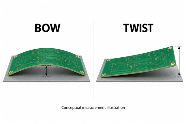
Bow is a roughly cylindrical or spherical curvature in which the corners of a rectangular board remain in one plane. Twist is diagonal deformation: three corners can touch a reference plane while the fourth is raised. Local coplanarity describes height variation within a defined region, such as a BGA land field or the mounting area for a power module.
Condition
What changes
Useful measurement basis
Bow
The board curves along its length or width while the corners remain approximately coplanar
Maximum gap divided by the relevant board dimension
Twist
One corner rises relative to the plane formed by the other three corners
Corner displacement and diagonal length using the specified method
Local coplanarity
A defined pad, component or mounting region departs from its local datum plane
Profile map, CMM or optical measurement over the stated area
Dynamic warpage
Board shape changes as temperature changes
Thermal-profile measurement with the agreed support condition
The phrase PCB warpage is often used broadly for bow, twist and temperature-dependent shape change. A PCB bow and twist specification is appropriate for room-temperature bare-board acceptance, but it should not be treated as proof of local BGA coplanarity or behavior during reflow.
Why Does Flatness Matter During PCB Assembly?
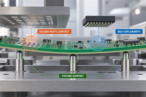
Assembly equipment assumes a predictable relationship between the board, stencil, placement head and support system. Excessive deformation can reduce contact between the stencil and pads, change solder-paste release, shift the focal plane for inspection, or leave a large package with uneven stand-off. Press-fit connectors, edge-card contacts and enclosure features can also become difficult to align.
For fine-pitch assemblies, our HDI PCB manufacturing and PCB assembly services can be reviewed together. The board construction, solder-paste process, package coplanarity and underside support all affect the result. A flat bare board does not eliminate every assembly variable, and a fixture that forces a board flat can hide its free-state deformation.
Mechanical interfaces create another constraint. If a PCB must contact a thermal pad or metal baseplate, the drawing should define the mounting region and allowable gap rather than relying on a general statement such as “board must be flat.”
How Is PCB Flatness Measured?
A basic PCB flatness measurement places the bare board on a precision surface plate and uses feeler gauges, a height indicator or equivalent metrology to measure the gap. IPC-TM-650 Method 2.4.22 describes production and referee procedures for bow and twist percentage on rigid boards, rigid portions of rigid-flex boards and panels. Its scope does not establish the special support conditions needed for populated assemblies.
Measurement task
Typical equipment
Report should record
Go/no-go bow check
Surface plate and calculated feeler or pin gauge
Board length/width, permitted percentage and tested direction
Actual bow percentage
Surface plate, gauge set and dimensional measurement
Maximum gap, corresponding span and calculated result
Twist measurement
Surface plate, corner support and height gauge
Diagonal, raised-corner displacement and calculation method
Local surface profile
CMM, laser scanner or optical metrology
Datum, area of interest, point spacing and maximum deviation
Thermal warpage
Temperature-controlled optical measurement system
Temperature profile, support, side viewed and shape versus time
For bow, the percentage is the maximum gap divided by the measured length or width, multiplied by 100. Under the production twist method in IPC-TM-650 2.4.22, twist percentage is the measured raised-corner gap divided by twice the diagonal, multiplied by 100. A PCB bow and twist formula must therefore match the selected procedure. A PCB bow and twist calculator is only as reliable as its inputs; using the wrong span or fixture creates a precise-looking but invalid result.
Record the board dimensions, diagonal, measured gap, test side and restraint used for every PCB bow and twist measurement. This is more useful than reporting only a pass/fail label because it makes the result reproducible.
A documented PCB surface flatness check should also identify whether protective films, tooling tabs or breakaway rails remain on the sample. If measurements from the fabricator and assembler disagree, first compare sample state, reference plane, restraint and temperature before comparing numbers.
Which Flatness Limits Should You Put on the Fabrication Drawing?
A PCB flatness specification should state the controlling document and revision, product class where applicable, maximum bow and twist, test condition, sample state and any local coplanarity zone. A PCB flatness tolerance is meaningful only when those conditions are defined. “Meet IPC” alone is incomplete because several IPC documents address different products, methods and acceptance contexts.
For our FR4 boards, we list a bow-and-twist capability of ≤0.75%, subject to the stack-up, board size, thickness, material system, copper distribution and engineering review. This is a manufacturing capability statement, not an automatic limit for every design. A thin, long board, a mixed-material stack-up or a local interface may need a different requirement and a dedicated measurement plan.
Drawing item
Example of a clear instruction
Why it matters
Sample state
Routed bare board after final finish, rails removed
Prevents panel rails from masking individual-board shape
Global requirement
Maximum bow and twist per the named method and agreed percentage
Defines the overall acceptance calculation
Local requirement
Maximum plane deviation within a marked component or mounting area
Protects the interface that drives assembly performance
Thermal condition
Room temperature or specified temperature profile
Separates incoming inspection from reflow behavior
Reporting
Lot sample size, datum, instrument and measured result
Makes supplier and customer data comparable
IPC-6012 bow and twist requirements should be interpreted with the purchase documentation and applicable revision. If your product has a tighter enclosure, optics or thermal-interface requirement, put that requirement on the drawing instead of expecting the general board class to imply it.
What Causes PCB Warpage?
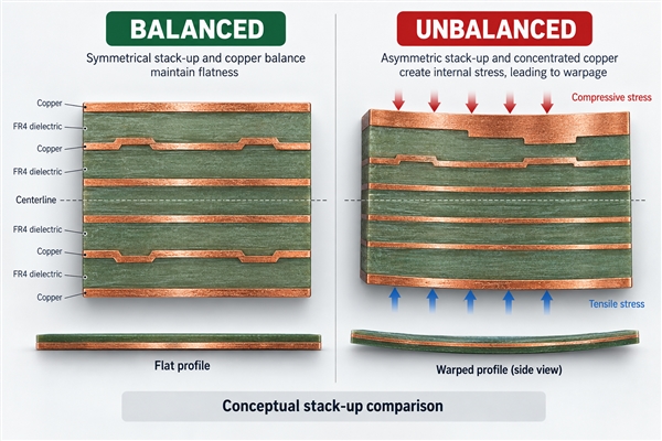
PCB warpage develops when stresses are not balanced through the board thickness or across the panel. Laminate resin, glass reinforcement, copper and surface coatings expand and contract differently. Lamination, oxide treatment, solder-mask curing, surface finishing and assembly reflow expose the construction to repeated heat and moisture changes.
Asymmetric stack-up: different dielectric thicknesses or copper weights above and below the centerline create unequal shrinkage.
Uneven copper distribution: a solid plane on one side and sparse routing on the opposite side can leave residual stress after cooling.
Material mismatch: hybrid high-frequency, metal-core or stiffener constructions can respond differently to temperature.
Thin or elongated geometry: low bending stiffness makes the same residual stress produce more visible deflection.
Panel and routing design: weak rails, uneven coupon placement, large cutouts and an unbalanced routing sequence can release stress unevenly.
Moisture and thermal history: storage, baking, solder-mask cure and reflow can change the free-state shape.
A PCB warpage calculation based only on laminate CTE cannot predict the final board. Copper pattern, resin flow, press cycle, panel position, routing and later assembly loads also matter. Use calculation to compare design options, then validate critical builds with representative coupons or samples.
How Do Stack-Up Symmetry and Copper Balance Reduce Warpage?
A mechanically balanced stack places similar copper weights and dielectric structures at comparable distances from the centerline. It does not require identical routing on every layer, but it avoids unnecessary imbalance in copper area and layer construction. This gives the laminate a more uniform response during pressing and cooling.
Our FR4 PCB manufacturing supports single-sided, double-sided and multilayer constructions up to 32 layers, subject to engineering review. More layers do not automatically improve or reduce flatness. What matters is the actual build: core and prepreg selection, copper weight, layer pairing, resin fill, overall thickness and panel utilization.
Copper thieving can improve local plating distribution and may help balance unused panel areas, but it is not a universal repair for an asymmetric product stack-up. We review copper distribution together with impedance, spacing and manufacturability so a flatness correction does not create an electrical or fabrication problem elsewhere.
How Do Board Thickness, Panelization and Routing Affect Flatness?
Thickness raises bending stiffness, so very thin boards are more sensitive to handling and residual stress. Our extra-thin PCB options include constructions from 0.15 mm, subject to material, size and engineering review. A thin-board requirement should therefore include panel support, assembly fixture and handling expectations rather than only the nominal thickness.
Panelization affects flatness before and after separation. Rails, crossbars, breakaway tabs, V-scores, routed slots and coupon placement change panel stiffness and the way stress is released. A large panel can pass while restrained by its frame, yet individual boards may change shape after routing. For flatness-critical parts, inspect both the production panel and the final routed board when those states serve different purposes.
Board outline matters too. Long narrow shapes, large internal windows and one-sided edge copper can create compliant regions. The best corrective action may be a stack-up change, panel rotation, added temporary support or revised routing sequence; simply increasing the final thickness can conflict with connectors, impedance or enclosure space.
Can PCB Surface Finish Improve Flatness?
A PCB surface finish can improve pad planarity relative to another finish, but it does not make the entire laminate flat. ENIG and immersion finishes deposit a comparatively uniform coating on exposed copper, while HASL can leave more variation across individual pads. This distinction matters for fine-pitch solder printing and probing.
However, the phrase PCB surface finish flat surface should not be interpreted as an overall warpage control method. Finish thickness is small compared with the board stack, and the chemical or thermal process cannot reverse a mechanically unbalanced construction. Select the finish for solderability, contact function, wire bonding, shelf life and pad-planarity needs; control global shape through the board design and fabrication process.
How Do We Control Flatness During PCB Manufacturing?
We begin with the released stack-up and panel, because most flatness risks are easier to prevent than to sort after fabrication. Our DFM review looks for asymmetry, concentrated copper, thin long geometry, mixed materials, large openings, unusual routing and local interfaces that deserve their own tolerance.
Confirm the applicable flatness definition, acceptance method and sample state.
Review layer symmetry, dielectric distribution and copper balance.
Plan panel rails, coupons, scoring or routing so the panel remains stable during processing.
Control lamination, curing and cooling according to the approved material and stack-up.
Inspect at the state that matters: panel, routed bare board and, when separately agreed, the assembly condition.
Use dimensional data to distinguish a design-driven pattern from a process or handling issue.
Our listed quality capabilities include 3D dimensional measurement, AOI, microsection analysis and electrical testing. These tools answer different questions. Flatness metrology measures shape; electrical testing checks continuity and insulation; microsectioning examines internal structure. One result should not be presented as proof of another.
What Should You Check After Reflow or Depaneling?
A room-temperature bare-board check is not the same as an assembled-board assessment. During reflow, the board becomes less stiff and materials expand at different rates. Components, solder, edge supports and fixtures add loads that are outside the basic bare-board bow-and-twist method. After cooling, some deformation recovers and some may remain.
When failure appears only after assembly, compare incoming flatness, panel location, paste printing, reflow profile, support-pin layout, component distribution and depaneling method. Measure the board both free and in its intended fixture if the product relies on mounting force. Record which condition produces the functional problem.
For a connector or thermal interface, inspect the actual local zone rather than averaging the entire board. For BGA-related opens, separate PCB shape from package warpage, paste volume and pad design before changing the fabrication limit.
What Information Should You Send for a Flatness-Critical PCB Order?
Send the fabrication files and a controlled drawing that identifies the critical flatness requirement. A complete manufacturing package includes:
Finished board dimensions, outline and panel preference
Layer count, proposed stack-up, copper weights and finished thickness
Material system and any mixed-material or stiffener construction
Maximum bow and twist, controlling method and sample state
Local coplanarity area, datum, maximum deviation and inspection method
Assembly process, peak thermal exposure and fixture constraints
Critical components, connectors, heat spreaders and enclosure interfaces
Required report format, sample size and lot traceability
At EBest Circuit (Best Technology), we will review the requirement against the actual board construction instead of treating one percentage as universal. Send your files and target PCB surface flatness criteria to sales@bestpcbs.com. We can align the drawing, manufacturing plan and assembly risk before production planning.
J-STD-003 addresses the solderability of bare printed circuit boards: whether the exposed surfaces intended for soldering can be wetted by molten solder. For your PCB project, that matters before components reach the assembly line. At EBest Circuit (Best Technology), we connect PCB fabrication and assembly support so that the board finish, component layout and soldering process are considered together.
What Is J-STD-003?
IPC J-STD-003 (also written IPC J STD 003 or J STD 003) is the solderability test standard for printed boards. Its subject is the board’s exposed conductors, attachment lands and plated-through holes, rather than component leads or completed solder joints.
Solderability testing helps separate a surface-wetting problem from an assembly-process problem. A satisfactory bare-board result does not prove that every joint will form correctly during production: solder paste deposition, component placement and the thermal profile remain separate parts of assembly quality.
Why Can a PCB Look Clean but Solder Poorly?
A clean-looking pad is not necessarily a readily wettable pad. Thin oxidation or contamination can interfere with the solder-to-metal interface without producing an obvious defect in an ordinary board photograph.
On our FR4 printed circuit boards, the solderable features include both surface-mount pads and connection points for through-hole parts. If solder withdraws from a pad, the resulting connection can be incomplete even though the copper circuit passes an electrical continuity test. Continuity and wettability answer different questions.
Appearance also depends on the solder alloy. Lead-free solder does not necessarily spread or look like tin-lead solder, so a comparison based only on shininess can be misleading. The important distinction is whether the intended metal surface has been wetted under the applicable test conditions.
Which Solderability Test Methods Are Used?
J-STD-003D includes visual evaluation methods and wetting-force measurement. The method must suit the board features being assessed.
Method family
Main evaluation
Edge dip
Wetting of exposed surface conductors
Surface-mount simulation
Wetting of surface-mount lands
Wave solder or solder float
Solderability of plated-through-hole features
Wetting balance
Wetting behavior recorded as force over time
For a board carrying both fine-pitch components and connectors, a surface-pad observation cannot answer every question about the holes. Likewise, a test on an unrelated reference board cannot establish the condition of your production lot. Representative material and the agreed evaluation method are essential to a useful result.
What Does a Wetting Balance Test Measure?
A wetting balance test records the force acting on a specimen as it contacts molten solder. The force-time response shows how wetting develops, adding information that a photograph taken after cooling cannot provide.
The response reflects surface tension, buoyancy and the developing solder meniscus. Test temperature, alloy, flux and specimen geometry affect the signal; curves obtained under different conditions are not automatically comparable. The illustration shows the measurement principle, not a measured result or a pass/fail limit.
For a difficult-to-solder pad, this measurement can help investigate delayed or weak wetting. It does not identify the root cause by itself, and it does not replace examination of the finish or the actual assembly process.
How Do Nonwetting and Dewetting Differ?
Nonwetting means solder has not formed the intended wetted interface. Dewetting describes solder withdrawing after initially covering an area, leaving an uneven coating. Both can reduce useful solder coverage, but they describe different behavior.
Observation
What it suggests
What it does not prove
Solder beads beside an uncovered pad
Possible nonwetting of that surface
That the PCB finish is the sole cause
Irregular solder islands after coverage recedes
Possible dewetting
A specific contamination source without further analysis
Smooth-looking solder on only part of the feature
Incomplete coverage still needs evaluation
Acceptance based on appearance alone
For an assembly defect, the PCB pad and the component termination should be distinguished. A board can have satisfactory solderability while a component lead has a separate surface problem. Adding more heat or flux without identifying the affected interface can damage the assembly rather than resolve the cause.
How Does PCB Surface Finish Affect Solderability?
The surface finish protects exposed copper and establishes the surface presented to the soldering process. ENIG, OSP, immersion silver, immersion tin and HASL use different protection systems, so the finish name alone cannot describe every assembly constraint.
Finish
Relevance to assembly
Project consideration
ENIG
Flat nickel-gold finish for component lands
Finish integrity and the planned soldering sequence
OSP
Organic protection over copper without a raised solder coating
Handling, storage and cumulative thermal exposure
Immersion silver or tin
Thin metallic protection on exposed copper
Packaging and finish-specific assembly conditions
HASL or lead-free HASL
Solder coating on exposed features
Pad planarity and alloy compatibility
For our HDI boards, fine-pitch pad geometry makes surface planarity and solder-paste deposition particularly relevant. A readily wettable finish cannot compensate for a stencil opening that delivers too little paste. Our finish options include ENIG, ENEPIG, OSP, immersion silver, immersion tin and lead-free HASL; we match the available construction to your board and assembly requirements.
Can Storage and Repeated Heating Change the Result?
Yes. The condition of a solderable surface can change between fabrication and assembly. Packaging, handling and thermal exposure therefore matter alongside the original finish selection.
A double-sided assembly may expose the second-side pads to heat before they are soldered. A later selective-soldering operation adds another thermal stage. These histories differ from soldering a fresh, unheated specimen, and their effect depends on the finish and process.
For boards held in storage, the production date alone is not a complete description of their condition. Whether the original packaging stayed intact and whether surfaces were exposed to contamination are also relevant. Baking should not be treated as a universal way to restore solderability: a moisture-removal step cannot simply reverse oxidation or damaged surface chemistry.
Is J-STD-003 Class 3 the Same as Coating Durability?
No. J-STD-003 Class 3 concerns the product classification; coating durability is a separate rating. A higher product class does not automatically specify an aging treatment.
In J-STD-003D, coating-durability notation differs between Pb-containing and Pb-free finishes. Category 2 or Category 3 terminology must not be exchanged blindly with the lettered categories for another finish system. Your specified revision and finish determine the applicable requirements.
What Is the J-STD-003 Latest Revision?
The J STD 003 latest revision listed when this article was checked in September 2026 is J-STD-003D. Older J-STD-003B and J-STD-003C references still appear in drawings and search results; they should not be treated as interchangeable editions.
If an existing design calls for an earlier revision, changing its acceptance basis is an engineering decision, not just a document-name update. We work from the agreed fabrication requirements rather than silently substituting a newer edition.
How Is J-STD-003 Different from J-STD-002 and J-STD-001?
The main difference is what is being evaluated: the bare board, the component connection surface, or the assembled soldered connection. The related standards are complementary, not substitutes.
Standard
Primary subject
J-STD-003
Printed-board solderability
J-STD-002
Solderability of component leads, terminations and related connection surfaces
J-STD-001
Requirements for soldered electrical and electronic assemblies
J-STD-004
Soldering flux requirements
J-STD-005 / J-STD-006
Solder paste / electronic-grade solder alloys and related forms
For example, a connector joint joins a board barrel to a component pin. Evaluating the barrel does not establish the pin’s solderability, while evaluating both surfaces still leaves the production soldering process to be controlled. This is why one bare-board test result cannot stand in for complete assembly acceptance.
How Do We Connect Bare-Board Quality with PCB Assembly?
We provide PCB fabrication and PCB assembly services, including SMT, through-hole and mixed assembly. This lets us consider the solderable board surface together with the components and the planned assembly sequence.
Our FR4 manufacturing capability extends to 32 layers, with the final construction subject to engineering review. For a multilayer controller with dense surface-mount parts and through-hole connectors, the board stack-up, pad finish and thermal demands all affect how fabrication and assembly fit together. We review these requirements as a connected PCB project, not as an isolated finish choice.
Discuss your J-STD-003 requirement with our engineering team at sales@bestpcbs.com. We can review the fabrication drawing, surface finish and assembly plan, and confirm the applicable project requirements before production. Any dedicated test method, sampling arrangement or report requirement must be agreed for that project.
IPC-SM-840C is the C revision of the specification for qualifying permanent solder mask used on printed circuit boards. It connects the coating’s electrical, physical and environmental performance with its intended application. For your PCB, the practical questions are which mask class applies, how the coating fits the layout, and whether it is compatible with fabrication and assembly. At EBest Circuit (Best Technology), we provide PCB manufacturing and assembly support to help turn those requirements into a buildable board.
What Is IPC-SM-840C?
IPC-SM-840C addresses the qualification and performance of permanent polymer solder mask, also called solder resist. The coating covers selected copper and laminate surfaces while leaving soldering pads, contacts and other specified areas exposed. It helps protect conductors and define where solder should wet during assembly.
The C revision dates to January 1996, with Amendment 1 issued in June 2000. It is a historical edition, so an existing drawing may name it even when a current material datasheet names a later revision. The standard concerns both material evaluation and the way the mask is used on a board. For example, a coating qualified on a test substrate still needs a suitable application process on the actual copper pattern.
What Do IPC SM 840 Classes T and H Mean?
Class T and Class H distinguish solder mask performance requirements by end-use reliability needs. Class T covers telecommunications and other high-performance commercial or industrial equipment. Class H addresses high-reliability applications where continued operation is critical. For drawings that specify IPC-SM-840C Class T or IPC SM 840C Class H, the required designation should carry through to the selected mask material.
Solder mask class
Application emphasis
What to specify for your board
IPC SM 840 Class T
Long service life in commercial and industrial electronics
Required revision, compatible mask material and intended assembly conditions
IPC SM 840 Class H
Higher assurance where uninterrupted operation is essential
Required revision and class, with the qualification evidence applicable to that material and process
These letters describe the solder mask requirement. The finished PCB’s IPC-6012 Class 2 or Class 3 requirement is a separate specification covering the rigid board. Keeping both requirements explicit makes the intended coating performance and overall board quality clear.
Which Solder Mask Properties Affect PCB Reliability?
Adhesion, electrical insulation and resistance to processing exposure determine whether the coating can protect the circuit throughout manufacture and use. Colour and surface appearance matter for inspection and product presentation, but the functional properties are the basis for material selection.
Property group
What it addresses
Relevance to the finished PCB
Adhesion and mechanical integrity
Bonding to the underlying surface; resistance to cracking or peeling
Maintaining coverage around tracks, pads and machined edges
Electrical performance
Dielectric strength and insulation resistance
Helping preserve insulation between neighbouring conductors
Soldering and chemical resistance
Exposure to soldering heat, fluxes and process chemicals
Keeping the mask intact through board finishing and assembly
Environmental performance
Moisture exposure, thermal changes and electrochemical migration
Matching the material to the board’s service conditions
Cure and surface condition
Developed film properties and usable surface quality
Supporting consistent handling and subsequent processing
For our FR4 printed circuit boards, solder mask selection belongs alongside copper layout, surface finish and assembly requirements. A controller with exposed test points has different mask artwork needs from a densely populated communications board, even when both use the same laminate family.
How Does LPI Solder Mask Become a Protective Pattern?
Liquid photoimageable solder mask is applied as a coating and patterned by light exposure and development. A typical LPI soldermask process includes surface preparation, coating, preliminary drying, imaging, development and final cure. The result is a permanent film with openings matched to the circuit artwork.
Surface preparation supports adhesion; imaging and development define the openings; final cure develops the required film properties. Their combined effect explains why the material name alone is only part of the finished-board result. Dry-film photoimageable solder mask offers another material format, with different behaviour over the board’s raised copper features.
The phrase LDI vs LPI solder mask can cause confusion: LPI describes liquid photoimageable material, while laser direct imaging describes an imaging method. An appropriately formulated LPI material can be used with direct imaging. Material selection and imaging compatibility therefore need to be considered together.
What Is the Recommended Thickness for PCB Solder Masks?
The recommended finished thickness is material- and layout-specific; one universal value does not describe every PCB. Solder mask thickness affects protection over copper edges, available clearance and the local surface height around component pads. A patterned PCB is not flat: copper traces, planes and gaps create different coating conditions. Thickness over a conductor and thickness beside it may therefore differ.
An IPC SM 840 solder mask thickness requirement should identify the measurement location and the agreed finished-film requirement. A value measured over bare laminate is not directly interchangeable with one measured over copper. The material system, copper profile and circuit geometry determine the practical coating window.
This becomes especially relevant on our heavy copper PCBs: taller conductors make edge coverage and coating transitions more demanding. Providing the outer-layer copper requirement with the mask artwork allows these features to be considered together, rather than treating the mask as a uniform flat sheet.
Why Do Pad Openings and Mask Dams Matter?
Pad openings expose the intended solderable surface, while a solder mask dam is the narrow strip of coating between adjacent openings. Registration is the alignment between the mask pattern and the copper pattern. Together, these features influence usable pad area and separation around fine-pitch components.
For our HDI boards, the pad pitch, opening size and achievable registration must work together. If a proposed dam is too narrow to manufacture consistently, the layout or opening strategy needs adjustment. The package’s land-pattern requirements remain important, particularly when choosing solder-mask-defined or non-solder-mask-defined pads.
Via tenting is a separate artwork choice: mask covers the via opening rather than filling the hole. Keep probe-access test points exposed, and specify via filling separately where that structure is required. These details help us preserve both assembly access and the intended coverage during DFM review.
How Do Surface Finish and Assembly Affect Mask Selection?
The mask must tolerate the selected board-finishing process and subsequent assembly exposure. ENIG, immersion tin and HASL use different chemical or thermal processing routes. Reflow, wave soldering and cleaning add further conditions after the bare board has been manufactured.
We offer finishes including ENIG, lead-free HASL, OSP, immersion silver and immersion tin. Sharing your intended finish and assembly route helps us discuss the appropriate board construction and mask compatibility. For a mixed SMT and through-hole assembly, the total processing sequence matters more than considering one reflow pass in isolation.
Mask colour can also affect imaging and cure settings within a material family. A green-to-black or green-to-white change is therefore a material/process choice as well as a cosmetic one. Its effect on fine features should be reviewed with the board requirements.
Solder Mask vs Conformal Coating: What Is the Difference?
Solder mask protects selected areas of the bare PCB and defines soldering openings. Conformal coating is normally applied after assembly to protect the populated board from its environment. They occupy different places in the build and can be used together.
For an industrial sensor exposed to humidity, the bare board may use solder mask while the completed assembly receives a compatible conformal coating. Connectors and test interfaces can require selective exclusion from that later coating. Adhesion between the two coatings and compatibility with cleaning residues become part of the assembly design.
Our PCB and PCBA services let you discuss bare-board manufacture and assembly as a connected project. Where additional protective coating is required, include that requirement with the assembly information so the intended materials and exposed areas are clear.
IPC SM 840 Latest Version: Is Revision C Still Current?
No. As of September 2026, the IPC document revision table lists revision E, issued in December 2010, after revision D from April 2007. C remains relevant to legacy specifications, but new project documentation should identify the edition actually required.
In the IPC SM 840 family, IPC SM 840C was followed by IPC SM 840D and IPC SM 840E. Revision E’s scope includes flexible cover materials as well as permanent solder mask. The revision letter therefore conveys technical scope, not merely a newer publication date.
If your drawing calls for C and the proposed mask documentation references E, send both with the project files. We can discuss the specified material and manufacturing route with you; any change to the drawing’s requirement should be agreed before production. The selected edition and class provide a clearer requirement than simply writing “IPC solder mask.”
How Can We Support Your PCB Solder Mask Requirements?
We combine PCB manufacturing, DFM support and assembly services, helping you match the solder mask pattern to the actual circuit. Our FR4 capability extends to 32 layers, and our HDI capability includes minimum line/space down to 2/2 mil, subject to materials, stack-up, board dimensions and engineering review. These are circuit-fabrication capabilities; the mask opening and dam requirements are reviewed separately.
For a board specified to IPC-SM-840C, send the Gerber files, fabrication drawing, required class, mask colour, surface finish and any critical pad or via details. Add assembly files when PCB assembly is part of the project. Contact our team at sales@bestpcbs.com or through our PCB manufacturing enquiry page to discuss your board.
IPC-6012 class II identifies a performance level for rigid printed circuit boards used in dedicated-service electronics. Usually written Class 2, it addresses the quality of the manufactured bare board, including its conductors, plated holes, insulation and structural integrity. It is not simply an appearance grade. At EBest Circuit (Best Technology), we manufacture PCBs and help you connect the specified performance class with a practical board construction, so your assembly starts with the right foundation.
What Is IPC-6012 Class II?
IPC-6012 Class II means the Class 2 requirements within the qualification and performance specification for rigid printed boards. Class 2 serves equipment where dependable operation and an extended service life matter, but uninterrupted operation is not as critical as it is for Class 3 applications. The numeral II does not mean a two-layer board or revision two of the standard.
IPC 6012 class 2 can apply to different rigid constructions, from a double-sided controller board to a multilayer interconnect. Layer count, laminate grade and surface finish still need their own specification. A Class 2 designation therefore answers one important question about acceptance, but does not define every feature of your PCB.
Which Products Are Suitable for Class 2 PCBs?
Class 2 is a relevant starting point for many commercial instruments, communications peripherals and industrial controls whose service requirements match dedicated-service electronics. The application name alone does not determine the class: the consequence of failure and the required operating conditions matter more.
Application example
What the PCB contributes
What still needs application-specific attention
Commercial measurement instrument
Stable connections between sensing, conversion and display circuits
Leakage paths, noise-sensitive layout and calibration requirements
Communications peripheral
Interconnects for processing, power and external interfaces
Controlled impedance, connector loading and signal integrity
Non-safety-critical industrial controller
Reliable mounting and connections for control and input/output circuits
Temperature cycling, contamination and terminal mechanical loads
For these types of circuits, our FR4 printed circuit boards provide a manufacturing route from prototypes to multilayer builds. We review the board design against the requested construction; an instrument’s safety function or environmental exposure may require additional requirements beyond a general Class 2 designation.
What Do IPC 6012 Class 2 Requirements Cover?
IPC 6012 class 2 requirements cover the finished bare board’s physical and electrical quality, not just its visible surface. The areas below explain why a board can look acceptable yet still need evidence about its internal connections or insulation.
Quality area
Examples of relevant features
Value to your product
Conductors and spacing
Trace geometry, copper continuity and separation
Maintains intended current paths and reduces short-circuit risk
Holes and interconnections
Hole copper, registration and connection to internal lands
Supports reliable connections between layers and component leads
Laminate and structure
Bonding integrity and response to specified thermal stress
Reduces vulnerability to internal damage during subsequent processing
Solderable surfaces and mask
Surface condition, coverage and mask alignment
Provides a suitable foundation for component assembly
Dimensions and flatness
Finished geometry, hole position, bow and twist
Helps the board fit fixtures, connectors and the enclosure
Electrical performance
Continuity and insulation-related requirements
Checks conditions that appearance cannot establish
The applicable revision and your agreed drawing determine the actual acceptance limits. Our PCB testing capabilities include AOI, microsection analysis and flying-probe testing. These address different types of evidence; a continuity pass alone does not demonstrate every structural requirement.
Why Are Hole Copper and Annular Rings Important?
A plated hole is an electrical connection through the board, while its annular ring is the copper land around the hole. Their geometry and integrity affect whether a connection remains reliable after soldering and use. Drilling, layer registration and plating all contribute to the finished result.
The copper weight chosen for a surface layer is not the same measurement as hole-wall plating thickness. Likewise, a round pad in the design file does not guarantee the same annular ring after drill and registration tolerances. Preserving manufacturing allowance around these features helps avoid late layout changes and marginal interconnections.
For our HDI boards, the connection between a microvia and its target land is also important. A small surface footprint can save routing space, but microvia construction needs its own engineering review; it should not be treated as a scaled-down conventional through-hole with identical behavior.
How Do Laminate and Thermal Stress Affect Reliability?
The laminate must maintain insulation and structural integrity through the thermal conditions relevant to the build. Copper and resin expand differently, so soldering heat places stress on the board and its interconnections. This is why material selection and plated-hole quality work together rather than as separate purchasing choices.
Our high-Tg PCBs are relevant when the assembly and operating conditions call for a suitable higher-Tg laminate. However, Tg alone is not a complete reliability rating: moisture behavior, thermal expansion, board thickness and the soldering profile also matter. A higher-Tg material does not automatically turn a Class 2 board into Class 3.
For your product, the useful distinction is between the specified board qualification evidence and the environment the assembled equipment will actually encounter. Repeated field temperature cycles or a harsh environment may need additional validation even when the bare board meets its agreed acceptance requirements.
IPC 6012 Class 2 vs Class 3: Which Fits Your Application?
The central difference in IPC 6012 class 2 vs class 3 is the required level of service performance and the associated acceptance criteria. Class 3 is intended for applications where continued operation is more critical. It is not simply the same board with a better finish or an extra final inspection.
Decision
Class 2
Class 3
Service expectation
Dependable operation and extended service
Higher-performance service where continued operation is critical
Design and fabrication impact
Features must meet the agreed Class 2 requirements
Some features need tighter acceptance conditions and corresponding manufacturing allowance
Project implication
Appropriate when product requirements fit this class
Needs early alignment of design, fabrication and qualification requirements
IPC 6012 class 1 addresses general electronic products and is not a substitute for a required Class 2 build. At the other end, specifying IPC 6012 class 3 does not by itself establish compliance with every medical, automotive or aerospace requirement. Relevant addenda and product-specific obligations can apply. Choosing the class early is more effective than trying to upgrade a completed lot through inspection alone.
How Does IPC-6012 Differ from IPC-A-600 and IPC-A-610?
IPC-6012 defines rigid-board qualification and performance requirements; IPC-A-600 helps interpret printed-board acceptability visually; IPC-A-610 concerns electronic assemblies. These documents address related but different parts of the product, so they are not interchangeable.
A solder joint on a mounted component belongs to the assembly discussion, whereas a plated hole inside the bare board belongs to board fabrication. If your project includes both PCB manufacture and assembly, we can support both stages, but each needs its appropriate acceptance basis. Our IPC-A-600 bare PCB inspection explanation describes how visual and internal observations complement performance requirements.
Does Class 2 Determine Layer Count, Finish or Impedance?
No. Class 2 is not a complete stack-up or electrical design. A board can require controlled impedance, a particular laminate or a specific surface finish in addition to Class 2 acceptance. Those choices come from the circuit and its assembly requirements.
For example, a communications board may need a defined impedance structure, while an industrial control board may place greater emphasis on current capacity and terminal spacing. Both can use a Class 2 acceptance basis without sharing the same construction. We offer FR4 builds up to 32 layers, subject to engineering review. We can discuss the stack-up, routing density and assembly needs together to identify a suitable construction for your design.
Early DFM support helps connect your intended circuit with manufacturable pads, holes and conductor geometry. It also makes special requirements visible before production, rather than leaving them to be inferred from a general class note.
Which IPC-6012 Revision Applies?
The IPC 6012 latest revision listed in the official revision table is IPC-6012F, September 2023, checked on September 11, 2026. The agreed revision for an existing product can differ. The letter identifies the edition; Class 2 identifies a performance level within that edition.
A legacy drawing referring to IPC 6012D class 2 should therefore not be silently treated as a Class 2 callout under revision F. Where your product moves to a newer edition, the affected requirements need to be aligned with the design and manufacturing agreement. Different editions of an IPC-6012 PDF are not interchangeable simply because they discuss the same class.
What Does IPC-6012 Certification Mean?
IPC-6012 certification can refer to different things, including an individual’s training credentials or a manufacturing qualification program with a defined scope. Neither should be confused with the conformity of a particular board lot. The certificate, issuing organization and scope determine what a certification claim actually establishes.
For the PCBs you receive, the useful evidence relates to the agreed board revision, specified class and applicable manufacturing or test records. A company-level quality certificate alone does not replace that product-specific evidence, and a bare-board acceptance result does not prove the completed equipment’s functionality.
How Can We Support Your Class II PCB Project?
We support PCB fabrication, DFM and PCB assembly, helping you carry the intended board requirements from design into a practical build. Our available inspection and test capabilities include microsection preparation and analysis, copper-thickness checks, AOI and flying-probe testing. Tell us which test reports your project needs so we can confirm the test scope and delivery documentation with your build.
Send your board files, fabrication drawing and intended application to sales@bestpcbs.com. At EBest Circuit (Best Technology), we can review your IPC-6012 class II requirements alongside the stack-up, material and assembly needs, so the board specification supports the product you are building.
Edge plating can create a conductive connection around a routed PCB perimeter, but the layout, net assignment and panel route must agree.
PCB edge plating is copper and final finish carried from the top or bottom conductor around a routed board edge. It is used for purposes such as RF shielding continuity, chassis grounding, mechanical contact or a plated boundary. The feature succeeds only when the copper artwork, board profile, solder-mask opening, net assignment and production panel all describe the same intent.
The safest design approach is to treat the plated edge as a manufactured three-dimensional feature—not as a decorative line on one Gerber layer. Define which edges are plated, which net owns them, where plating must stop and how the fabricator may support the board during processing. This PCB edge plating design guide turns those decisions into a DFM- and RFQ-ready package.
What Is PCB Edge Plating and When Is It Worth Using?
Edge plating wraps conductive metal over a selected external board edge so it connects intended copper features on the board faces. Depending on the design, it can close part of an RF shield boundary, provide a low-inductance connection to an enclosure, create a durable contact surface or join top and bottom ground regions along the perimeter.
It is worth specifying when the electrical or mechanical function genuinely requires a plated routed edge. It is not automatically better than perimeter vias, a metal frame, a connector shell or castellated holes. Each alternative creates a different current path, assembly interface and manufacturing constraint.
Good candidates: RF modules fitted into conductive housings, shielding partitions, grounding rails and board edges intended to contact a conductive chassis.
Questionable candidates: cosmetic gold edges, edges broken by many panel tabs, mixed-net copper near the route or designs without a defined mating interface.
Required decision: state the electrical purpose and the mating condition before drawing the feature.
Edge Plating vs Castellated Holes and Edge Contacts
These features can all expose metal at a PCB edge, but they solve different problems. Selecting the wrong one can create unnecessary cost or an interface that cannot be assembled reliably.
Feature
Main purpose
Key data to define
Continuous or selective edge plating
Conductive wrap, shielding boundary, chassis or mechanical contact
Plated segments, net, profile, panel breaks and finish
Castellated holes
Solderable half-holes for mounting one PCB onto another
Hole size, pitch, pad geometry, finished profile and assembly fillet
Edge-card contacts
Mating fingers for a connector
Contact pattern, bevel, finish, mask opening and connector tolerance
Via fence near an edge
Ground stitching and field containment without a plated route
Via pitch, return-path geometry and distance to profile
A design may combine a via fence with edge plating, but their roles should remain explicit. If the real requirement is a solderable board-to-board interface, use a controlled castellated-hole design rather than asking a fabricator to infer it from a plated outline.
How Edge Plating Supports RF Grounding and EMC
A grounded plated edge can reduce discontinuity around a board perimeter and provide a short connection between face copper and a conductive enclosure. This is useful where RF currents need a controlled return path or where an enclosure seam should not become an unintended slot antenna.
Edge plating is not a universal EMI cure. Its effect depends on the full current path: reference planes, stitching vias, enclosure contact pressure, apertures, connector bonding and the location of high-frequency sources all matter. A continuous-looking copper edge that is poorly connected to the intended reference can add metal without fixing the actual return-path problem.
Start with the electromagnetic function, then model or review the transition. The site’s RF PCB capability overview provides context for high-frequency board construction, while this guide focuses on the plated boundary itself.
Should the Plated Edge Connect to System Ground or Chassis Ground?
Assign the plated edge to the net required by the product grounding architecture; do not default to a generic ground symbol. Signal ground, protective earth and chassis can be joined directly, joined through a defined network or kept separate depending on safety, EMC and system requirements.
Show the plated edge on the schematic or controlled mechanical/electrical drawing with a named net.
Identify where the edge contacts the housing and whether contact is continuous or limited to selected zones.
Keep unrelated power or signal copper away from the plated route according to the approved DFM clearance.
Review connector shields and mounting hardware as parts of the same grounding path.
If chassis and circuit ground are intentionally separated, mark the isolation boundary clearly.
For high-frequency designs, the via pattern that connects surface copper to internal reference planes may be as important as the plated edge. Ask for a stackup-aware review instead of applying a copied spacing rule from another board.
How to Draw Edge Copper in the PCB Layout
Draw copper to the intended finished outline on the participating outer layers and identify every plated segment unambiguously. Exact artwork conventions vary by fabricator and CAD export, so the released drawing must explain how the data should be interpreted.
Create the final board profile on a single authoritative mechanical layer.
Extend the intended top and/or bottom copper to the selected profile segment.
Assign the copper to the correct ground, chassis or functional net.
Add the required stitching connection to internal planes where the electrical design calls for it.
Stop all different-net copper before the route using the fabricator-approved clearance.
Mark start and stop points for selective plating, especially near cutouts and connectors.
Add a detail view showing the wrap direction and finished condition.
Do not place an oversized copper flood around the entire outline if only two short edges need plating. Selective geometry makes electrical review, panel planning and inspection clearer.
Where Solder Mask Must Open Along the Plated Edge
Solder-mask data must expose the metal that is intended to wrap or make contact, while protecting adjacent copper that should remain insulated. The opening should be coordinated on both board faces and around corners or cutouts included in the feature.
Define whether the exposed band is a functional contact surface or simply part of the manufacturing wrap. If a metal enclosure, spring finger, gasket or conductive adhesive will touch it, show the actual contact footprint and tolerance zone. Keep silkscreen legends and reference text out of that interface.
Do not publish a universal mask expansion value. Registration capability, profile tolerance, finish and board construction differ. Request the approved relationship among finished edge, outer-layer copper and mask opening during DFM.
How to Keep Edge Connectors and Different-Net Copper Safe
The plated route must not unintentionally bridge a connector contact, mounting feature or nearby conductor. Edge-card fingers, coaxial launches, antenna structures and chassis contacts deserve an explicit keep-out review.
Separate plated segments from edge-card fingers and their bevel region.
Mark every intentional electrical break in the edge plating.
Review plated slots or cutouts independently from the external perimeter.
Check copper on all layers, not only the visible outer faces.
Confirm that a router transition or corner radius will not leave a copper bridge.
Include mounting holes, metal hardware and conductive gaskets in the clearance analysis.
Why Panel Tabs and Routed Breaks Must Be Planned
Edge plating requires access to the board edge, while production panels require material that holds the board during fabrication and assembly. A support tab placed through a functional plated segment interrupts the finished metal and can leave a rough breakout. A fully plated perimeter may therefore conflict with the proposed panel route.
The designer does not need to invent the factory panel, but should identify critical no-tab zones and acceptable break locations. The fabricator can then choose a routed panel, temporary support strategy or agreed interruptions compatible with its process.
Panel concern
Possible result
Data needed
Tab crosses plated segment
Missing metal or rough witness after depanelization
Critical continuous zones and permitted breaks
Insufficient handling support
Board movement or process instability
Array drawing and assembly handling needs
Late profile revision
Copper and route no longer align
One released outline revision
Corner or cutout ambiguity
Unplated gap or unintended bridge
Enlarged edge detail and finish callout
Panel support, routed openings and connector keep-outs must be reviewed together with the plated segments.
How Material, Thickness and Edge Geometry Affect Feasibility
Feasibility depends on the specific stackup, board thickness, copper construction, profile geometry and factory route. Straight external edges are generally easier to define and inspect than narrow internal cutouts, acute corners or small isolated plated segments.
Before quotation, ask the supplier to confirm the proposed edge feature against the released stackup. Items that may change the route include hybrid RF materials, very thin or thick boards, heavy outer copper, sequential structures, controlled-depth features and tight mechanical interfaces.
EBest Circuit’s exact limits for a particular edge-plated build should be treated as to be confirmed through the original capability data and project DFM review. Do not assume that a value used on one material, plant or special process applies to every order. The broader PCB design for manufacturability guide explains why stackup and profile constraints should be reviewed together.
Which Surface Finish Should Be Specified?
Select the finish from the electrical contact, solderability, durability, storage and system requirements—not from edge plating alone. A plated edge that only completes a shield boundary may have different wear requirements from a repeated mechanical contact.
State whether the edge is a mating contact, solderable feature, enclosure interface or non-contact shield boundary.
Identify any wear, corrosion, bonding or conductivity requirement.
Confirm that the chosen finish can be applied consistently to the intended edge geometry.
Keep connector fingers and their finish specification separate when they use a different construction.
Define inspection expectations for coverage and exposed base copper.
For a general comparison of finish choices, use the PCB surface-finish selection guide. The final selection still requires project-specific confirmation.
What Gerber Layers and Fabrication Notes Should Show
A quote-ready package identifies the plated segments in both machine-readable artwork and a human-readable drawing. Do not rely on an email sentence after the data has been released.
Provide Gerber, ODB++ or another agreed manufacturing dataset.
Include one controlled board-profile layer with slots and cutouts.
Show outer-layer copper reaching each intended plated edge.
Show solder-mask openings associated with the feature.
Label the electrical net and any deliberate breaks.
Dimension critical contact zones, no-tab zones and mating locations.
Specify surface finish and the expected finished appearance.
Add a fabrication note such as “plate only the highlighted routed edges; all other edges remain unplated,” then reference the correct detail.
Include a neutral 3D image or PDF detail for communication if useful, but make the controlled fabrication data authoritative. The PCB fabrication specifications checklist can help organize the rest of the build package.
Which DFM Failures Cause Gaps, Peeling, Shorts or Rough Edges?
Most edge-plating failures begin as a disagreement among the electrical design, mechanical profile and panel route. Review the failure mechanism before changing only the visible copper artwork.
Symptom
Likely question
Prevention
Gap in a critical segment
Did a tab, route transition or artwork break cross the edge?
Define continuous zones and review panel support
Unintended short
Was another net or connector feature too close to the plated route?
Run all-layer clearance and net checks
Peeling or weak adhesion
Does the copper construction and process support the geometry?
Confirm stackup and edge preparation with the fabricator
Rough breakout
Was a functional surface used as a depanelization point?
Move tabs or define an acceptable non-contact break
Finish does not cover as expected
Was the edge included in the finish and inspection callout?
State the finished condition and acceptance criteria
How Should Edge Plating Be Inspected and Accepted?
Acceptance should address coverage, continuity, isolation, finish and mechanical interface. Visual appearance alone cannot prove the intended electrical function.
Verify the correct edges and only those edges are plated.
Inspect critical segments for gaps, exposed base material, blisters, peeling and rough damage.
Check isolation from different-net copper and adjacent connector contacts.
Measure continuity or resistance where the drawing defines an electrical requirement.
Fit-check the enclosure, spring contact or gasket when the edge is a mechanical interface.
Record first-article photographs of critical corners, breaks and contact zones.
Agree in advance how permitted panel-break witness marks will be judged.
For RF hardware, functional verification may also include enclosure-level EMC or RF testing because a good-looking edge cannot compensate for gaps elsewhere in the shield or return path.
What Changes Edge-Plating Cost and Lead Time?
Cost and lead time depend on plated length and complexity, stackup, routing, panel support, finish, inspection and first-article requirements. Selective straight segments with clear data are easier to assess than a nearly continuous perimeter broken by connectors, tabs and internal cutouts.
Ambiguous data adds engineering exchanges and can delay quotation. A special panel strategy, unusual finish, tight contact tolerance or additional electrical/mechanical inspection can add setup and processing time. Ask suppliers to separate non-recurring engineering or tooling from recurring unit cost so quotes can be compared on the same assumptions.
What to Send for an Edge-Plating RFQ
The RFQ must let the supplier reconstruct the electrical, mechanical and manufacturing intent without guessing. Send:
Gerber or ODB++ data, drill files and one authoritative board profile.
Stackup, material selection, finished thickness and copper requirements.
A drawing that highlights every plated segment and intentional break.
The plated-edge net and its connection to planes or stitching vias.
Solder-mask openings, connector keep-outs and enclosure contact zones.
Permitted and prohibited panel-tab locations.
Surface finish and any wear, bonding or corrosion requirement.
Quantity, prototype or production stage and target delivery date.
First-article, continuity, dimensional and visual acceptance requirements.
BOM, CPL and assembly drawings when fabrication and assembly will be quoted together.
Label unresolved items as “supplier to confirm” rather than silently assuming a factory limit. That makes the DFM response part of the controlled engineering record.
FAQ About PCB Edge Plating
Is PCB edge plating the same as castellated holes?
No. Edge plating creates a conductive wrap along a routed edge, while castellated holes form solderable half-holes for board-to-board assembly. Their artwork and acceptance criteria differ.
Does edge plating always need to connect to ground?
No. Grounding is common for shielding and chassis interfaces, but the correct net follows the product architecture. State the intended net explicitly.
Can an entire PCB perimeter be edge plated?
Potentially, but production panel support and depanelization must still be solved. A nominally continuous perimeter may require agreed breaks or a special handling route.
Can edge plating improve EMC?
It can support a shorter, more continuous shielding or return path, but EMC performance depends on the entire enclosure, planes, via stitching, connectors and apertures.
Should copper extend to the board outline?
For intended edge-plated segments, outer-layer copper is typically designed to meet the finished route according to the fabricator’s data convention. Confirm the exact artwork rule during DFM.
Should solder mask cover a plated PCB edge?
A functional plated contact normally requires a coordinated mask opening. The correct opening depends on the intended contact and the supplier’s registration and process rules.
Why do panel tabs matter?
A tab can interrupt a plated segment and leave a rough witness after breakout. Mark critical no-tab zones and permitted breaks before the array is finalized.
Which surface finish is best for edge plating?
There is no universal choice. Select the finish from conductivity, wear, solderability, corrosion and mating requirements, then confirm it for the edge geometry.
How is edge plating inspected?
Inspection can include visual coverage, continuity, isolation, dimension and fit with the mating enclosure or contact. Define the required evidence in the drawing or quality plan.
What is the most important RFQ detail?
A marked fabrication detail showing exactly which edges are plated, their net, the finish and acceptable panel breaks. Without it, the supplier must guess at the core requirement.
Need a PCB quote with edge plating?
Send EBest Circuit your Gerber/ODB++ files, stackup, plated-edge drawing, net assignment, surface finish, panel constraints, quantity and acceptance requirements. We will review the project data and confirm the applicable manufacturing route before quotation.
PCB immersion gold is usually an ENIG surface finish: a thin gold layer over electroless nickel on exposed copper pads. It offers a flat solderable surface and protects the nickel before assembly. It is a useful choice for many fine-pitch boards, but it is not the same as wear-resistant hard gold. The right decision depends on how the pads will be soldered, contacted, stored and inspected.
What Is Immersion Gold PCB Surface Finish?
ENIG stands for electroless nickel immersion gold. The copper carries the circuit, nickel forms the barrier beneath the finish, and gold protects that nickel from oxidation. An electroless nickel immersion gold PCB therefore has a layered coating on selected exposed conductors, not a solid-gold circuit board. An ENIG PCB retains copper as its main circuit conductor.
The terms immersion gold finish, ENIG finish and chemical nickel/gold commonly describe this construction. A gold plated circuit board is a broader description: it might use ENIG, electrolytic hard gold or another gold-containing finish. Color alone cannot identify the process, thickness or intended application. Our ENIG process overview provides further background on this finish family.
Is direct immersion gold the same as ENIG?
No. Direct immersion gold places gold directly on copper, without the electroless nickel layer that defines ENIG. It is a different finish architecture. Confirm the full coating stack whenever a drawing uses only “immersion gold”; this article focuses on the conventional ENIG construction.
How Does the PCB Immersion Gold Process Work?
The PCB immersion gold process normally follows copper patterning and solder-mask preparation. Exposed copper is cleaned and prepared, electroless nickel is deposited, and a controlled immersion reaction deposits the gold coating. Rinsing, drying and inspection complete the finish. The exact preparation sequence depends on the qualified chemistry and board materials.
In conventional immersion gold plating, gold deposition involves a displacement reaction at the nickel surface. It does not require the external electrical connection used by electroplating. The process must balance coverage against excessive nickel attack; simply leaving a board in the bath longer is not a sound way to request better quality.
What does electroplated gold mean?
It means gold is deposited using an externally supplied electrical current. PCB gold plating can use that method to build a specified contact finish, including hard gold plating. Electroless gold plating is a broader chemistry term and should not be used to erase the difference between autocatalytic deposition and immersion displacement. Specify the actual process, not just “Au plating.”
What Does Each ENIG Layer Do?
The three metals have different jobs. Copper is the underlying conductor. Nickel separates copper from the outer gold and provides the interface beneath the solderable finish. The gold cap protects the nickel during the intended pre-assembly life, but it is not an impermeable environmental seal.
During normal soldering, the thin gold coating is incorporated into the solder and the joint develops at the underlying nickel-containing interface. The finished joint should not be imagined as a solder ball resting on a permanent gold barrier. This is why nickel condition matters even when an ENIG circuit board looks uniformly gold.
How Thick Should PCB Immersion Gold Be?
Specify nickel and gold separately. Nickel thickness is on the micrometer scale, while immersion gold thickness is much smaller, typically discussed in hundredths of a micrometer. A requirement stating only “gold thickness” leaves the barrier layer and measurement method unresolved.
For unit checking, 1 microinch = 0.0254 micrometer; therefore, 2 microinches is 0.0508 micrometer. This is a conversion example, not a recommended acceptance limit. Never confuse micrometers with microinches or apply a connector hard-gold requirement to ENIG solder pads.
PCB immersion gold thickness requirements should identify the applicable IPC-4552 revision, agreed deposit limits, measurement locations and acceptance method. PCB ENIG specifications should also distinguish process-control targets from lot-acceptance criteria. Do not combine figures from different revisions or treat a single measurement as proof of process consistency. A brighter surface does not demonstrate a thicker or better deposit.
Does “IPC 4552 Class 3” define every acceptance condition?
No. The phrase identifies a standards-related requirement but is not a complete coating specification. State the revision and applicable product requirements, then confirm how deposit thickness, nickel corrosion and solderability will be assessed. Class selection does not authorize an arbitrary increase in gold thickness.
Why Choose ENIG for Fine-Pitch Assembly?
An ENIG surface finish is relatively planar, which can help solder-paste printing and component seating on closely spaced lands. This is valuable for BGA, QFN and other fine-pitch packages where an uneven finish can complicate assembly. Flatness is a useful starting condition, not a guarantee against bridging, voids or poor joints.
For HDI printed circuit boards, finish selection belongs alongside pad geometry, microvia construction and solder-mask registration. ENIG does not fill an open via-in-pad or correct a badly defined land pattern. Those features require their own manufacturing controls.
An immersion gold FR4 PCB need not be high density. On double-sided FR4 circuit boards, the same finish may be selected for flat pads and a planned assembly-storage window. Choose it because those requirements matter, not because a gold plated PCB board automatically performs better electrically.
PCB Immersion Gold vs Hard Gold Plating
ENIG is primarily selected for solderable pads and qualified low-wear interfaces. Hard gold is selected when contact wear and repeated mating drive the specification. These are different engineering jobs even if both surfaces appear gold.
Requirement
ENIG / immersion gold
Hard gold
Primary role
Flat solderable finish and qualified contacts
Wear-resistant electrical contact surface
Deposition
Electroless nickel with immersion gold cap
Usually electrolytic gold alloy over nickel
Repeated insertion
Not a default substitute for connector plating
Specify thickness, hardness and mating conditions
Soldering
Normal use when finish and assembly are qualified
Must be assessed for the specific deposit and joint
A board may need selective hard gold on edge fingers and a different finish on solder pads. Keep these areas explicit in the fabrication definition. Do not approve a substitution using only the word “gold,” and do not assume a thin immersion coating will survive a connector’s full mating-cycle requirement.
ENIG vs HASL and OSP: Which Finish Fits?
Comparing PCB surface finish types starts with the assembly process. Lead-free HASL leaves a solder-alloy coating; OSP is an organic copper surface finish; ENIG adds nickel and gold. These PCB surface finishes protect exposed PCB surfaces differently.
Finish
Main reason to consider it
Important limitation
ENIG
Planar metallic finish for fine-pitch pads
Nickel corrosion and deposit control require attention
Lead-free HASL
Established solder-coated finish
Surface unevenness can constrain fine-pitch assembly
OSP
Flat organic protection with soldering to copper
Handling and the complete thermal process need qualification
Immersion silver or tin
Other planar metallic alternatives
Storage, environment and assembly compatibility differ
The ENIG vs HASL decision is not simply expensive versus cheap. Compare the cost of the completed assembly, including yield and handling. OSP can also support demanding assembly when its chemistry and process are qualified; it should not be dismissed as universally unsuitable for multiple reflows. PCB finish types must be evaluated against the actual build.
ENEPIG vs ENIG: When Does Palladium Help?
ENEPIG adds an electroless palladium layer between nickel and gold. It is relevant when a design combines soldering with demanding wire-bonding requirements, particularly where the bonding process needs a suitably qualified surface. ENEPIG vs ENIG should therefore be decided using the wire material, bonding method and assembly sequence.
Do not assume every ENIG board is unsuitable for all wire bonding, or that every ENEPIG deposit guarantees a successful bond. Aluminum or copper wedge bonding and gold wire bonding are different processes. ENIPIG is another named finish variant, not a spelling-equivalent specification; identify the intended palladium deposition route before accepting a substitution.
What Causes Black Pad in ENIG Plating?
Black pad is associated with excessive nickel corrosion in the ENIG process and can contribute to poor solder-joint integrity. Gold coverage can conceal the affected interface, so a normal-looking surface does not rule it out. At the same time, discoloration alone does not prove black pad.
Control requires a qualified combination of surface preparation, nickel deposit characteristics, gold-bath condition and process monitoring. If a joint fails, investigate the interface and fracture evidence rather than assigning the cause from a photograph. More gold is not a universal remedy and can increase cost without solving the underlying issue.
How Do You Inspect an Immersion Gold PCB?
Use complementary checks. Optical inspection finds visible coverage and surface defects; calibrated thickness measurement evaluates deposits; solderability testing examines wetting under defined conditions. None replaces all the others.
Inspect pads for missing coverage, contamination, extraneous plating and abnormal discoloration.
Measure nickel and gold using equipment and calibration appropriate to the coating stack and pad geometry.
Sample representative locations rather than only the easiest large pad.
Review corrosion evidence using the specified qualification or acceptance method.
Evaluate solderability after the relevant storage or thermal exposure when required.
Keep lot identification and inspection results tied to the delivered boards.
X-ray fluorescence can measure coating thickness when the instrument and model are suitable. It does not independently establish solder-joint strength or exclude every corrosion defect. Likewise, a bare-board open/short test verifies electrical connectivity, not the complete quality of the PCB surface treatment.
How Long Is Immersion Gold PCB Shelf Life?
Immersion gold PCB shelf life depends on the qualified finish, packaging, storage environment, handling and the acceptance test. There is no unconditional storage period that can be assigned from the letters ENIG alone. Follow the fabricator’s stated conditions and maintain lot traceability.
Handle boards by their edges, avoid touching solderable pads and keep unopened packaging intact until needed. After exposure to humidity, contamination or an extended storage interval, review solderability before committing a production lot. Baking is not a universal reset for a damaged or contaminated finish; any drying or recovery process must be compatible with the board and coating.
What Changes for Flex and High-Frequency Boards?
An immersion gold flexible PCB still needs a bend-aware design. Nickel-containing finish in a repeatedly flexed region can become a mechanical concern; define where the finish is exposed and where bending occurs. For rigid-flex circuit boards, keep solder-pad requirements distinct from the dynamic flex region and validate the intended bend conditions.
For an immersion gold high-frequency PCB, evaluate the complete metallization stack on RF-critical exposed conductors. Nickel can affect conductor loss, depending on frequency and geometry. The presence of a gold cap does not automatically make a transmission line lower loss. Model or measure the real stack instead of assigning a universal frequency cutoff.
A multilayer PCB with immersion gold normally receives its finish on the exposed outer features. Inner-layer copper is not automatically coated with ENIG. Internal layer count and surface finish are separate manufacturing choices.
What Drives Immersion Gold PCB Price?
Immersion gold PCB price reflects exposed finishing area, specified deposit, process control, panel utilization, board construction and order quantity. Precious-metal cost matters, but it is not the only cost. Additional selective finishes, inspection requirements and difficult feature geometry can change the total.
Compare equivalent constructions and acceptance conditions. A lower price for a different nickel/gold specification is not a like-for-like saving. Nor should a standard ENIG quotation be treated as a commitment to hard-gold connector performance or specialized wire bonding.
Our Manufacturing Support for ENIG Boards
At EBest Circuit (Best Technology), we support ENIG alongside lead-free HASL, OSP, immersion silver, immersion tin, hard gold and ENEPIG options. We review the PCB plating choice together with the land pattern, materials and assembly needs, rather than treating the finish as a cosmetic upgrade.
Our FR4 fabrication capabilities include multilayer boards up to 32 layers, and our assembly capabilities include SMD components down to 01005 and BGA pitch down to 0.25 mm, subject to material selection, stack-up, board dimensions, design complexity and engineering review. These capabilities are not a guarantee that every combination is manufacturable or that ENIG alone ensures assembly yield.
Conclusion
Choose PCB immersion gold when its flat solderable surface and qualified storage performance fit the product. Define the nickel and gold layers, distinguish solder pads from wearing contacts, and verify both the finish and the assembly process. Contact our team at sales@bestpcbs.com for manufacturing support with the appropriate board construction and surface finish.
A coil on pcb can be formed by routing a copper trace into a spiral, loop or multilayer winding. Unlike a separate wire-wound component soldered to a board, this printed inductor is part of the PCB itself. Its behavior depends on the artwork, copper thickness, layer stack-up and nearby materials. A useful design therefore needs more than an inductance value: resistance, operating frequency, coupling and temperature must also work in the finished assembly.
What Is PCB Coil?
A PCB coil is a conductor patterned on a circuit board to produce a useful magnetic field or inductance. The phrase may also refer loosely to a mounted inductor coil, so first establish whether the winding is etched copper or a purchased component. This article focuses on the etched version, also called a planar inductor or printed coil.
A flat PCB coil normally has two electrical terminals, not a set of independent concentric rings. One terminal begins at the outer turn; the inner terminal often uses a via and a trace on another layer to escape without crossing the winding. A coil PCB can carry surrounding electronics, or it can be a separate sensing or antenna board. A planar PCB coil is therefore a physical winding structure, not a separate component footprint.
What Does a Coil Do in a Circuit?
A coil stores energy in a magnetic field and opposes changes in current. A changing field can also induce voltage in another conductor. These effects let coils act as inductors, antennas, sensors, transformer windings or actuators, depending on their connection and geometry.
The ideal relationships are v = L di/dt and E = 0.5 L I2. A real PCB inductor adds resistance and parasitic capacitance, so it cannot be treated as ideal at every frequency. What is a coil in electronics? It is the winding that provides this magnetic behavior, not necessarily a cylindrical wire component.
Printed Coil vs Wire-Wound Coil
Choose a printed winding for repeatable geometry and low profile; consider a discrete winding when inductance, current or magnetic-core requirements would consume too much board area.
Design factor
Printed PCB coil
Wire-wound coil
Geometry
Set by copper artwork and board stack-up
Set by wire, winding and optional core
Height
Can be integrated within board thickness
Usually extends above the mounting surface
Resistance
Constrained by trace length and cross-section
Wire gauge and winding space offer different trade-offs
Inductance per area
Limited for a small air-core spiral
A suitable magnetic core can increase inductance
Change control
Requires revised artwork or stack-up
A compatible discrete part may be substituted after validation
Do not replace a power inductor with an inductor coil on PCB based only on matching nominal inductance. Compare its current waveform, losses, temperature rise, saturation behavior if a core is used, and required transient response. Our guide to inductor placement and selection on PCB covers the separate mounted-component case.
Which Dimensions Control PCB Coil Design?
Outer size, inner opening, turns, trace width and spacing must be considered together. More turns can raise inductance, but fitting them into a fixed footprint can increase resistance and capacitance enough to reduce useful performance.
Outer dimensions: influence magnetic-field coverage and available winding area.
Inner opening: determines how tightly the center is filled; tiny inner turns can add more loss than useful coupling.
Trace width: trades conductor resistance against the number of turns that fit.
Spacing: must account for fabrication tolerance as well as electrical interaction.
Copper thickness: changes resistance, etching behavior and finished trace shape.
Shape: circular, square and rectangular patterns have different field distributions and model coefficients.
For a simple single winding with a bottom-layer escape, double-sided printed circuit boards provide a practical construction. Keep the escape route short and avoid routing it across the active winding on the same copper layer.
How Should You Use a PCB Coil Calculator?
A PCB coil calculator provides a starting estimate, not a finished-board guarantee. Match its model to the shape and layer count, then enter actual manufacturable dimensions. A circular-coil equation should not be applied unchanged to a long rectangular winding.
A PCB coil inductance calculator typically requires turn count, trace width, spacing and inner or outer dimensions. A PCB rectangular coil inductance calculator must also represent both axes. A multilayer PCB coil calculator needs the layer separations and winding connections; simply multiplying a single-layer result ignores mutual coupling.
For a first-order series model, Q = 2 pi f L / RAC, sufficiently below self-resonance. Use AC resistance at the intended frequency, not only a multimeter’s DC resistance. For an LC circuit, f0 = 1 / (2 pi sqrt(LC)) is an initial estimate; the effective capacitance includes the attached circuit and parasitics.
A PCB coil generator or PCB coil design program can automate artwork, but exported tracks still need connectivity and manufacturing checks. Confirm the winding belongs to the intended net, both terminals are accessible, and no polygon fill or copper bridge shorts adjacent turns.
How Do Multilayer PCB Coils Connect?
A multilayer PCB coil can connect windings in series or parallel, but current direction determines whether their fields reinforce or oppose. Follow the entire current path through every via rather than judging polarity from how a spiral looks on screen.
For two series-connected windings, the inductance is L1 + L2 + 2M when the fields aid, and L1 + L2 – 2M when they oppose. Multilayer PCB coil design also changes interlayer capacitance and self-resonance. Parallel windings require balanced connections and current distribution; their benefit is not captured by a universal layer-count multiplier.
An embedded coil PCB places a winding on internal copper layers. Lamination protects it mechanically, but dielectric thickness and surrounding copper become part of its electromagnetic environment. A PCB bifilar inductor coil uses two closely associated windings; specify their electrical relationship rather than treating all adjacent traces as one series spiral.
Should Copper or a Ground Plane Sit Under the Coil?
Nearby conductive material can alter inductance and introduce eddy-current loss. A solid plane beneath a sensing loop may reduce the very field interaction the design needs. Review adjacent layers, shielding, mounting hardware and the enclosure, not just the visible top copper.
Use a deliberate copper keepout where the application requires an exposed magnetic field, and keep sensitive signal returns outside that keepout correctly routed. Do not remove an entire board’s reference plane without considering return paths. Some applications intentionally use shielding or a magnetic sheet; those features must be included in the model and prototype.
For higher-frequency resonant circuits, RF printed circuit boards allow material and construction choices suited to the circuit. A low-loss laminate does not cancel winding resistance or guarantee a target Q. Low-frequency sensor coils may work well on ordinary FR4 after validation.
What Is a Coil Used For?
PCB coils are useful when their geometry can be matched to sensing, coupling or actuation. The application defines the right compromise, not a universal number of turns.
Inductive sensing: target movement changes the electrical response of the coil and its readout circuit.
NFC and RFID: a loop couples to a reader field; tuning and the final enclosure influence operation.
Wireless power: transmitting and receiving windings exchange energy through magnetic coupling.
Current measurement: a PCB Rogowski coil surrounds a conductor and responds to changing current.
Motion: a PCB coil motor uses patterned stator windings interacting with a magnetic rotor.
A PCB Rogowski coil sensor is not just a flat spiral placed anywhere near a wire. PCB Rogowski coil design uses an appropriate closed sensing path and signal conditioning; its induced voltage depends on current change, so steady DC cannot be measured by the coil alone. For motor-specific construction, see our PCB stator motor design guide.
Can a PCB Coil Work as an Electromagnet?
A PCB coil electromagnet produces a field when driven with current, but useful force depends strongly on the magnet or target, air gap, geometry and thermal limit. A shallow printed winding is not automatically a replacement for a high-force solenoid.
For PCB power coil design, estimate copper loss as P = IRMS2R using resistance appropriate to temperature and waveform. Check temperature in the actual duty cycle and enclosure. A copper coil on PCB may need wider tracks or thicker copper, but additional copper does not remove all AC losses.
heavy copper printed circuit boards are relevant when conductor resistance and current handling dominate, including suitable planar transformer windings. Their trace-width and spacing requirements differ from fine-line boards. A PCB coil transformer also needs isolation, coupling and, where applicable, magnetic-core design beyond the winding artwork.
Can You Use a PCB Coil for Wireless Charging?
A wireless charging coil on PCB is possible, but feasibility depends on power, frequency, coupling, losses and thermal performance. A thin printed winding may suit a restricted-height design while being less efficient than a purpose-designed wire or litz-wire winding in another system.
For a PCB wireless charging coil, measure the coupled pair at the expected alignment and separation, including any ferrite and shielding. A proposed Qi PCB coil must meet the applicable system requirements; merely drawing a spiral does not establish Qi compatibility. NFC antenna operation at 13.56 MHz is a different design problem from wireless power transfer and should not inherit its tuning network.
How Do You Test a Coil on PCB?
Test connectivity first, then measure inductance and losses at the relevant frequency, and finally verify the complete application. Passing a DC continuity check alone does not establish useful coil performance.
Inspect trace spacing, terminal escape and vias for opens or cross-turn bridges.
Measure DC resistance with suitable lead compensation; use a four-wire method when resistance is low.
Measure inductance and Q with an appropriate LCR meter or impedance analyzer, compensating the fixture.
Sweep frequency when self-resonance or RF behavior matters.
Repeat with the final enclosure, target, shield or receiving coil installed.
Check temperature rise and response over the intended operating range.
If the result differs from the model, check units, layer spacing, terminal routing, test leads and nearby metal before adding turns. A shorted turn can change inductance substantially while the two terminals still show continuity.
Further Questions About Printed Coils
Can a Rogowski coil on PCB measure steady DC?
No. Its output responds to changing current and normally needs integration to reconstruct the measured AC waveform. A PCB inductor coil used as an energy-storage element has a different function from this current-sensing structure.
What happens when you coil a wire?
The fields from individual turns interact, usually increasing useful inductance compared with the same wire laid straight. Winding spacing, shape and a magnetic core influence the result. PCB traces use the same physical principle with a different conductor geometry.
What is the role of a coil in electronics?
Its role can be energy storage, filtering, coupling or sensing. Identify the connected circuit before deciding whether a coil on circuit board is a power component, an antenna or a sensor.
Can several coils on PCB share one readout?
They can in a designed multiplexed or multichannel system. Switching parasitics, mutual coupling and channel calibration must be included; connecting every coil in parallel is not a general solution.
Is an air-core printed coil free from all current limits?
No. It lacks a ferromagnetic core that could saturate, but copper heating, dielectric limits, driver capability and nearby materials still limit operation.
Our PCB Coil Manufacturing Support
At EBest Circuit (Best Technology), we review the winding geometry together with the board construction. Our FR4 capabilities include ordinary minimum line/space of 4/4 mil and multilayer constructions up to 32 layers, subject to materials, dimensions, stack-up and engineering review. These are fabrication capabilities, not a promise that the finest trace or highest layer count produces the best coil.
We can support copper-thickness checks, optical inspection and open/short electrical testing. Coil inductance, Q, coupling and temperature acceptance require a project-specific test definition; they are not implied by a standard bare-board continuity test.
Conclusion
A reliable coil on pcb starts with the required magnetic function and finishes with measurement in its real surroundings. Keep the current path continuous, use a geometry-appropriate model, control losses and verify the finished stack-up. Contact sales@bestpcbs.com to discuss manufacturing support for your printed winding and surrounding circuitry.
Blind vias connect an outer copper layer to an internal layer without passing through the entire PCB. Use them when dense component escape routing or an unwanted signal stub creates a problem that ordinary through vias cannot solve efficiently. They can free routing space, but add constraints to drilling, plating, stack-up and inspection. The right choice is the simplest manufacturable interconnection that meets the circuit’s needs.
What Is a Blind Via?
A blind via is a circuit board via with one end at an external surface and the other at an internal target layer. A blind via hole is therefore accessible from one board face but does not open onto the opposite face. For example, an L1-L2 connection in a six-layer board is blind; an L1-L6 connection is through.
For background, PCB vias are conductive connections between copper layers, not unplated mounting holes. Questions such as “what is a via?” or “what are vias?” concern this basic vias meaning; a blind via adds the condition that the connection stops inside the board.
A blind via PCB can contain other types of vias too. Using blind vias in PCB routing does not mean every connection must be blind. Through vias may remain appropriate for connectors, power distribution or signals needing a different layer span.
The construction is determined by the finished board, not only by the drilling operation. A hole drilled through a subassembly may become blind after additional layers are laminated to that subassembly.
What Is the Difference Between Blind and Buried Vias?
Blind vias and buried vias differ in whether they reach a finished board surface. A buried via connects internal layers only. Its connection must be manufactured while those layers are accessible, before they are enclosed by later lamination.
Connection
Finished-board span
Useful when
Main trade-off
Blind via
Outer layer to internal layer
Surface component escape needs routing space below
Depth, plating and build sequence need review
Buried via
Internal layer to internal layer
Inner-layer routing should not consume outer pads
Hidden interconnects and additional processing
Through via
Entire board thickness
Conventional routing can tolerate its barrel and clearances
Unused barrel may form a stub; occupies more layers
The buried via vs blind via decision follows the required endpoints. A buried via hole cannot directly provide the top-surface connection of a component pad. Conversely, a blind via and buried via may be combined within the same HDI stack-up. These are complementary PCB via types, not competing quality grades.
Blind Via vs Microvia: Are They Different?
Yes, but the categories overlap. “Blind” describes the layers a connection reaches. “Microvia” describes a small, shallow interconnect structure, commonly laser formed in an HDI build-up layer. A surface-to-next-layer microvia is also a blind via; a mechanically drilled blind connection is not automatically a microvia.
In a microvia PCB, several short connections can be arranged across successive build-up layers. A deeper connection should not be called a microvia merely because its opening looks small. The hole formation process, depth, diameter and applicable qualification requirements must all agree.
The practical answer to microvia vs blind via is therefore not “choose one.” First choose the required layer span, then determine whether a shallow laser microvia or another qualified blind structure can realize it.
When to Use Blind Vias?
Use blind vias when they remove a specific routing or electrical limitation. Common reasons include escaping fine-pitch BGA pads into a nearby routing layer, preserving inner-layer channels, and shortening an otherwise excessive signal-via stub.
Dense surface routing: a short L1-L2 connection can move a signal away from a crowded pad field without reserving a through-hole clearance on every layer.
Constrained board area: recovering routing space can help when changing the enclosure or connector locations is not practical.
Controlled high-speed transitions: a shorter barrel may reduce the unused stub, provided the pad, antipad and return-path geometry are also suitable.
For our HDI printed circuit boards, interconnection planning starts with the component escape pattern and feasible build-up. Adding blind vias after routing is complete can force a stack-up redesign.
In compact rigid-flex circuit boards, dense connections may be needed in a rigid component area while the flexible section carries interconnects between assemblies. Any blind-via option requires construction-specific review. Do not extend a rigid-area via rule into a dynamic bend region or assume a via can sit at a rigid-flex transition without assessment.
Keep conventional through vias when they already satisfy routing, electrical and mechanical requirements. An HDI feature is not automatically an improvement on a simple board.
How Are Blind Vias Made?
The PCB blind via fabrication process depends on when the target layer is accessible. Shallow laser drilling is common for build-up microvias. Controlled-depth mechanical drilling or drilling a subassembly before further lamination can serve other blind structures.
Define the layer pairs, materials and fabrication sequence.
Form the hole to the intended copper target or through the relevant subassembly.
Clean the hole and prepare the dielectric and target-pad surfaces for metallization.
Deposit and build copper to create the electrical connection; fill and planarize when the specified construction requires it.
Complete subsequent imaging and lamination stages, then inspect and electrically test the finished connections.
Via hole drilling is only one operation in that sequence. A correctly located cavity can still fail if residue prevents adhesion at the target pad or copper deposition is inadequate. Blind/buried vias also require clear identification of each drill span; one undifferentiated drill file cannot adequately describe several different layer pairs.
In HDI PCB design, reaching deeper routing layers may require a chain of microvias through successive build-up layers. The outer connection is blind, while connections entirely inside the finished board are buried. These successive microvias can be vertically stacked or laterally staggered, so their arrangement belongs in the fabrication plan rather than being treated as an unrelated hole type.
How Do Stacked Vias Differ from Staggered Vias?
Stacked vias align successive microvias vertically. A stacked via structure saves lateral space, but introduces copper-fill and interfacial requirements at each level. Staggered vias offset successive connections and join them with an intermediate trace or pad region.
A staggered via layout uses more area but can simplify certain interconnect interfaces. Neither arrangement is automatically reliable or unreliable: the number of build-up levels, materials, process control and qualification evidence determine suitability.
The minimum blind buried via stagger distance cannot be selected as one universal number. It depends on capture and target pad diameters, registration tolerance, copper spacing and the manufacturer’s approved construction. Measure the clearance between real copper features, not only between drill centers.
What Blind Via Aspect Ratio Is Practical?
Define the ratio before comparing limits. Here, via aspect ratio = connection depth divided by drilled hole diameter. For a blind connection, use its own depth, not the full finished-board thickness. Some supplier tables express the inverse ratio, so a bare ratio without its definition is ambiguous.
As a geometry example, an 80-micrometer-deep opening with a 100-micrometer diameter has a depth-to-diameter ratio of 0.8:1. This calculation is illustrative, not a production limit. A shallower blind via aspect ratio generally makes cleaning and copper deposition easier, but material, taper, target-pad condition and plating method still matter.
Many laser-microvia processes use shallow geometries around or below 1:1, with the acceptable value set by the qualified fabrication process. Do not apply a general through-hole aspect-ratio capability to laser microvias. A “blind via ratio” requirement must state the dimensions and convention being used.
Finished opening size, drilled diameter and bottom diameter are not interchangeable. For deeper blind structures, consult the actual process limits rather than extrapolating a shallow microvia rule.
What Changes with Blind Via in Pad Designs?
A blind via in pad can provide a short escape route directly beneath a component termination. It also puts the hole treatment and surface condition inside the soldering interface. An open cavity may consume solder or affect joint consistency.
Specify the required filling, planarization and cap treatment for the actual assembly process. A capped via has a copper-covered surface, but that name alone does not describe the complete internal fill structure or guarantee a flat solderable land. Solder-mask tenting is not the same as copper filling and capping.
For fine-pitch pads, evaluate surface depression or protrusion, finish and solder-joint requirements together. Do not assume every PCB blind vias design requires identical filling, or that any filled hole is acceptable beneath any package.
Blind Via vs Backdrill: Which Solves the Problem?
The blind via vs backdrill comparison matters when an unused plated barrel is the main concern. Backdrilling removes an unwanted portion of an already plated through via using a larger controlled-depth drill. It reduces the stub but does not create the same build-up structure as a blind microvia.
A blind connection may also free routing space below its endpoint. A backdrilled hole still needs clearance for the larger drill and a controlled residual stub. If routing space is available and the issue is primarily signal integrity, backdrilling may be worth comparing with an HDI reconstruction.
On RF printed circuit boards, the substrate and complete transition geometry must be reviewed together. A short signal barrel alone does not establish a good RF transition: return connections, pad capacitance, antipads and material behavior remain important. We assess process compatibility for the selected laminate instead of assuming every RF material supports the same blind-via process.
For backdrill vs blind via decisions, compare the modeled transition, remaining stub tolerance, routing impact and fabrication sequence. Do not promise a fixed bandwidth improvement from the via name alone.
Are Blind Vias More Expensive?
Usually, compared with an otherwise similar conventional through-via board. Blind via cost can increase because of laser or depth-controlled drilling, additional lamination stages, copper filling, registration requirements and inspection. The premium is design dependent, not a fixed percentage.
Blind vias cost should also be considered at assembly level. If the construction removes unnecessary layers or enables a substantially smaller board, the system-level result may differ from the price of one fabrication operation. Compare manufacturable alternatives with the same functional requirements.
To control cost, use only the necessary layer spans, favor a repeatable build-up, and avoid specifying maximum density throughout areas that do not need it. Simplifying a stack-up early is usually more useful than trying to negotiate around an unnecessarily complex finished layout.
Which Blind Via Design Rules Should Be Checked?
Blind via design rules for printed circuit board vias must come from the agreed stack-up and fabrication process. A printed circuit board via needs the intended copper connection and isolation from unrelated nets. A CAD rule set is useful only when its assumptions match the intended manufactured structure.
Layer span: every via pair must have a feasible drilling and lamination sequence.
Depth and diameter: check the stated aspect-ratio convention and the relevant hole dimensions.
Capture and target pads: preserve registration allowance and the required copper connection.
Clearances: inspect adjacent traces, plane antipads and the actual spacing in dense escape areas.
Surface treatment: define fill, cap and flatness where vias share component lands.
Return path: ensure the signal transition has an appropriate nearby reference connection.
Our PCB via size guide provides additional terminology context. Its general hole-size discussion does not replace construction-specific blind-via approval.
How Can Blind Via Reliability Be Verified?
Use complementary checks. Electrical testing detects connectivity problems; cross-section inspection examines the physical interconnect. A sample that passes continuity today may still contain an interface weakness that appears after assembly or thermal cycling.
Verification
Purpose
Boundary
Stack-up and fabrication-data review
Confirm layer pairs, pad geometry and process sequence
Does not prove physical plating quality
Electrical testing
Identify opens and unintended shorts
Does not by itself establish fatigue life
Microsection examination
Inspect target-pad interface, copper distribution and fill
Samples selected locations, not every via
Assembly and thermal-stress qualification
Evaluate the selected construction under defined exposure
Results apply to the tested conditions and structure
Review misregistration, contamination, copper voids, interface separation and thermomechanical stress as possible failure mechanisms. The appropriate coupon, sample plan and stress profile depend on product requirements. X-ray inspection can complement the process, but not every interface defect is visible in a conventional X-ray image.
More Questions About Blind Vias
Can a four-layer PCB use blind vias?
Yes, where an approved stack-up and process support the required layer pair. A four-layer board is not automatically an HDI board, and its layer count alone does not prove that a particular blind via is manufacturable. Compare the routing benefit with the added processing before selecting it.
Can blind vias replace thermal vias?
Not automatically. Thermal vias conduct heat toward a copper region or heat-removal path. A blind connection ending at an internal plane does not by itself carry heat to the opposite surface. Evaluate the complete thermal path, copper area and assembly rather than substituting via names.
What should be checked for Altium blind vias?
For Altium blind vias, define the stack-up and intended drill pairs, apply the fabricator-approved constraints, and inspect the exported manufacturing data. The connections displayed in the layout must correspond to actual, unambiguous layer spans in the output. This is a design review principle, not a version-specific click-by-click tutorial.
What should be checked for KiCad blind vias?
For KiCad blind vias, confirm that the selected board setup and routing rules allow the intended structure, then review the drill outputs with their start and stop layers. A rendered hole in a 3D preview does not confirm its fabrication sequence. Editor behavior and supported options depend on the version being used.
What does skip via vs blind via mean?
A skip via bypasses an intermediate conductor level to reach a deeper target. It may also be blind when it starts at an outer surface. Skipping a layer changes drilling, isolation and plating demands; it is not a way to ignore depth limits. Have the specific construction qualified instead of treating it as an ordinary adjacent-layer microvia.
Our Blind Via PCB Manufacturing Support
At EBest Circuit (Best Technology), we support blind and buried interconnection planning with our HDI manufacturing capability. Our available constructions include 1+N+1, 2+N+2 and 3+N+3 build-ups, with HDI line/space down to 2/2 mil and minimum hole capability down to 0.10 mm, subject to materials, board dimensions, stack-up and engineering review. These limits are not a blanket approval for every layer span, aspect ratio or combined feature set.
We review the proposed construction against our PCB manufacturing capabilities before treating a design as production ready. Our aim is to support the required routing and electrical function with a feasible build sequence, suitable inspection and clearly defined acceptance requirements.
Conclusion
Choose blind vias for a demonstrated routing or transition problem, not simply because the option is available. Define the endpoints, compare conventional and HDI constructions, and review depth, plating, fill and reliability together. For construction and fabrication support, contact our team at sales@bestpcbs.com.
This website uses cookies to enhance your experience, remember your preferences, and help us understand how visitors use our site. You can accept all cookies, reject non-essential cookies, or manage your settings.
This website uses cookies to improve your experience while you navigate through the website. Out of these cookies, the cookies that are categorized as necessary are stored on your browser as they are essential for the working of basic functionalities of the website. We also use third-party cookies that help us analyze and understand how you use this website. These cookies will be stored in your browser only with your consent. You also have the option to opt-out of these cookies. But opting out of some of these cookies may have an effect on your browsing experience.
Necessary cookies are absolutely essential for the website to function properly. These cookies ensure basic functionalities and security features of the website, anonymously.
Cookie
Duration
Description
cookielawinfo-checkbox-analytics
11 months
This cookie is set by GDPR Cookie Consent plugin. The cookie is used to store the user consent for the cookies in the category "Analytics".
cookielawinfo-checkbox-functional
11 months
The cookie is set by GDPR cookie consent to record the user consent for the cookies in the category "Functional".
cookielawinfo-checkbox-necessary
11 months
This cookie is set by GDPR Cookie Consent plugin. The cookies is used to store the user consent for the cookies in the category "Necessary".
cookielawinfo-checkbox-others
11 months
This cookie is set by GDPR Cookie Consent plugin. The cookie is used to store the user consent for the cookies in the category "Other.
cookielawinfo-checkbox-performance
11 months
This cookie is set by GDPR Cookie Consent plugin. The cookie is used to store the user consent for the cookies in the category "Performance".
viewed_cookie_policy
11 months
The cookie is set by the GDPR Cookie Consent plugin and is used to store whether or not user has consented to the use of cookies. It does not store any personal data.
Functional cookies help to perform certain functionalities like sharing the content of the website on social media platforms, collect feedbacks, and other third-party features.
Performance cookies are used to understand and analyze the key performance indexes of the website which helps in delivering a better user experience for the visitors.
Analytical cookies are used to understand how visitors interact with the website. These cookies help provide information on metrics the number of visitors, bounce rate, traffic source, etc.
Advertisement cookies are used to provide visitors with relevant ads and marketing campaigns. These cookies track visitors across websites and collect information to provide customized ads.